T0@st
News Editor
- Joined
- Mar 7, 2023
- Messages
- 3,063 (3.89/day)
- Location
- South East, UK
| System Name | The TPU Typewriter |
|---|---|
| Processor | AMD Ryzen 5 5600 (non-X) |
| Motherboard | GIGABYTE B550M DS3H Micro ATX |
| Cooling | DeepCool AS500 |
| Memory | Kingston Fury Renegade RGB 32 GB (2 x 16 GB) DDR4-3600 CL16 |
| Video Card(s) | PowerColor Radeon RX 7800 XT 16 GB Hellhound OC |
| Storage | Samsung 980 Pro 1 TB M.2-2280 PCIe 4.0 X4 NVME SSD |
| Display(s) | Lenovo Legion Y27q-20 27" QHD IPS monitor |
| Case | GameMax Spark M-ATX (re-badged Jonsbo D30) |
| Audio Device(s) | FiiO K7 Desktop DAC/Amp + Philips Fidelio X3 headphones, or ARTTI T10 Planar IEMs |
| Power Supply | ADATA XPG CORE Reactor 650 W 80+ Gold ATX |
| Mouse | Roccat Kone Pro Air |
| Keyboard | Cooler Master MasterKeys Pro L |
| Software | Windows 10 64-bit Home Edition |
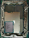
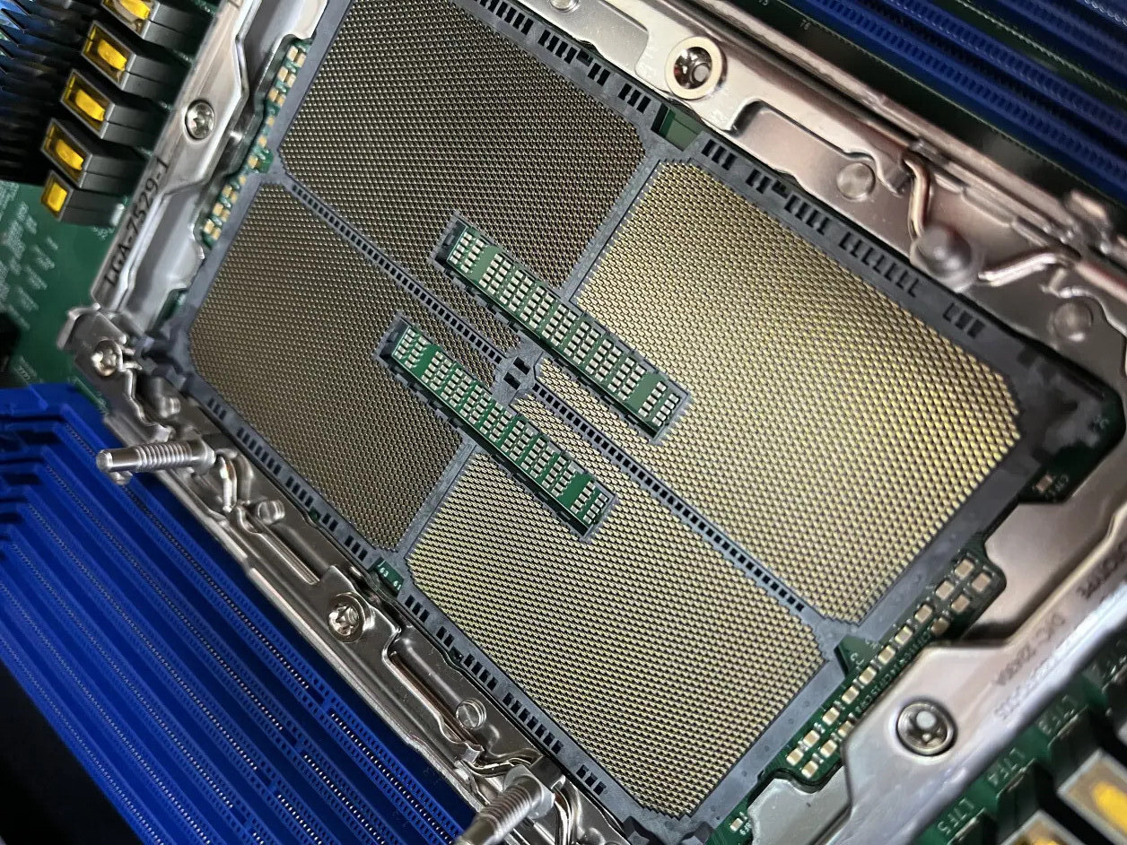
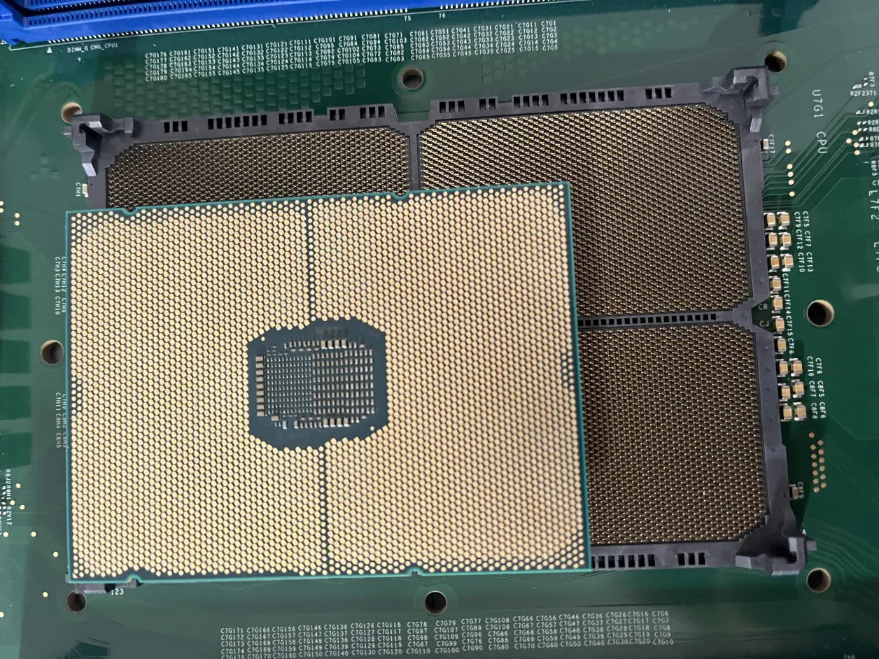
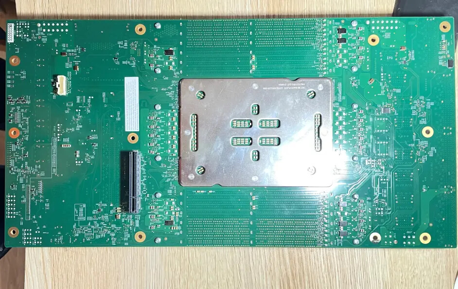
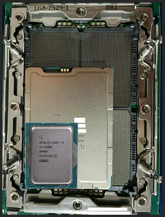
A set of detailed photos has been uploaded to a blog on the Chinese Bilibili site, and the subject matter is an engineering sample of a motherboard that features Intel's next generation LGA 7529 socket. Specifications and photos relating to this platform have cropped up in the past, but the latest leak offers many new tidbits of information. The Bilibili blogger placed a Sapphire Rapids Xeon Processor on top of the the new socket, and this provides an interesting point of reference - it demonstrates the expansive physical footprint that the fifth-generation platform occupies on the board.
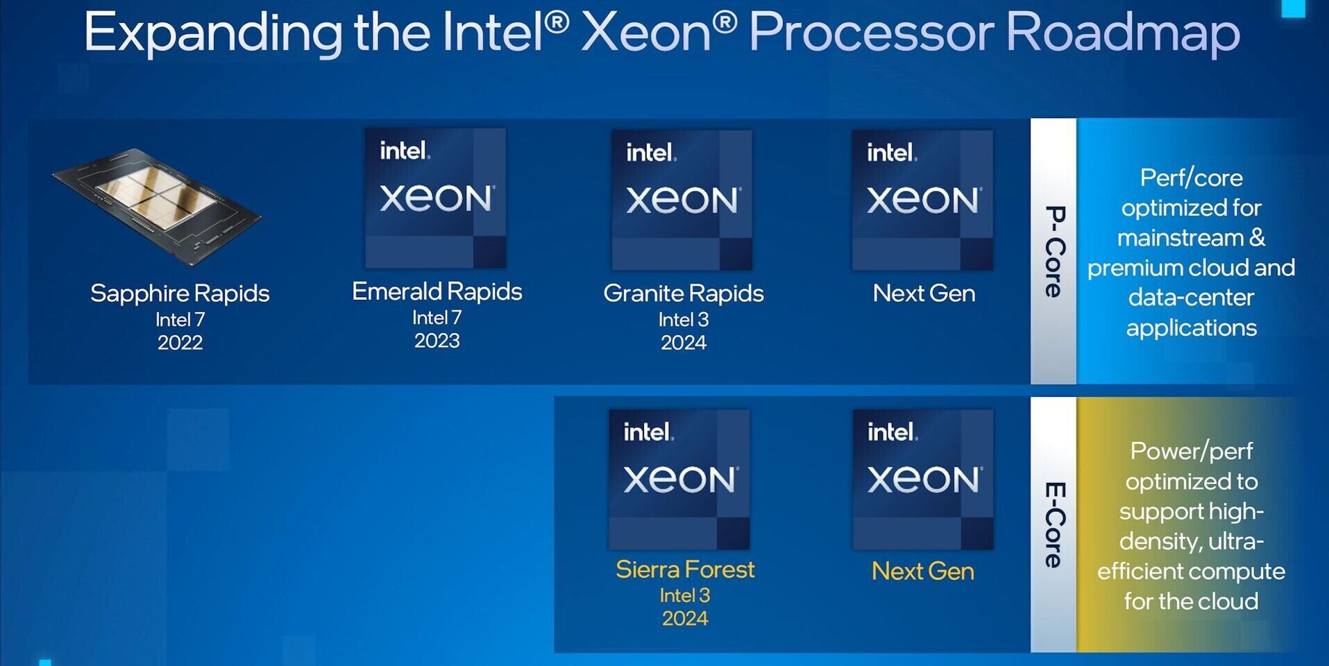
This year's Sapphire Rapids LGA 4677 (Socket E) is already considered to be a sizeable prospect - measuring at 61 × 82 mm. The upcoming Mountain Stream platform (LGA 7529) is absolutely huge in comparison, with eyeball estimates placing it possessing rough dimensions (including the retention arm) of 66 × 92.5 mm. The fifth generation platform is designed to run Intel's Granite Rapids and Sierra Forest CPUs - this family of Xeons featuring scalable microarchitecture is expected to launch in 2024. The code name "Avenue City" has been given to a reference platform that features a dual socket configuration.
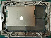

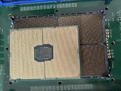
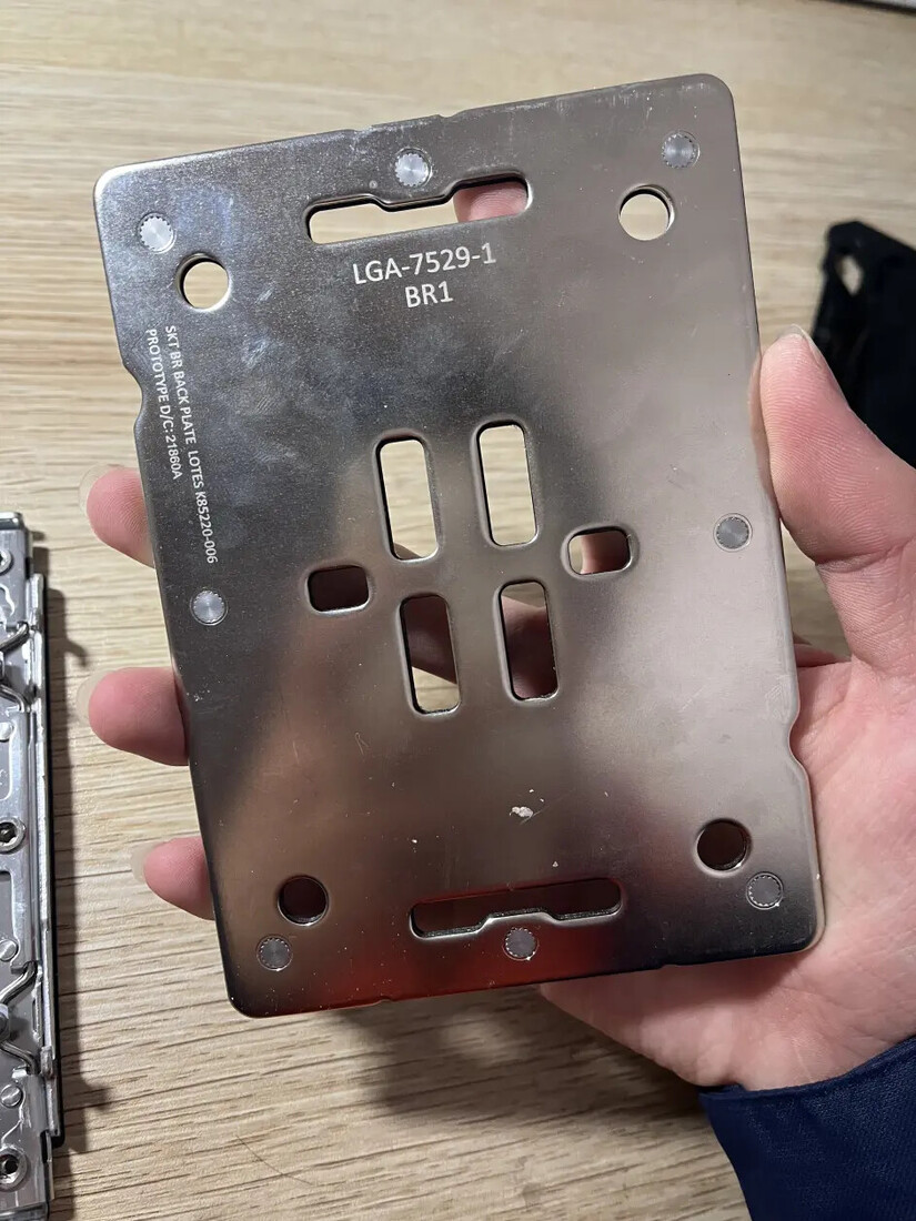
Based on an analysis of the single socket engineering sample motherboard, the leaker has theorized that this new Xeon platform will offer support for P-Core variants with up to 86 and 132 cores and E-Core variants with up to 334 and 512 cores, as well as HBM variants. The photographed board has "ES" labeled in multiple locations and stamping on the socket indicates that the whole package is a prototype manufactured by LOTES.


The leaker's findings align with past information that indicated Intel's plans for their forthcoming Granite Rapids and Sierra Forest Xeon processors. These ranges will diverge the Xeon family into two new offerings: one optimized for performance equipped entirely with P-cores, and the other for efficiency equipped with an E-core only array. Industry analysts are proposing that Intel will be targeting the high performance server and cloud computing sectors with these new offerings in 2024.


View at TechPowerUp Main Site | Source
This year's Sapphire Rapids LGA 4677 (Socket E) is already considered to be a sizeable prospect - measuring at 61 × 82 mm. The upcoming Mountain Stream platform (LGA 7529) is absolutely huge in comparison, with eyeball estimates placing it possessing rough dimensions (including the retention arm) of 66 × 92.5 mm. The fifth generation platform is designed to run Intel's Granite Rapids and Sierra Forest CPUs - this family of Xeons featuring scalable microarchitecture is expected to launch in 2024. The code name "Avenue City" has been given to a reference platform that features a dual socket configuration.
Based on an analysis of the single socket engineering sample motherboard, the leaker has theorized that this new Xeon platform will offer support for P-Core variants with up to 86 and 132 cores and E-Core variants with up to 334 and 512 cores, as well as HBM variants. The photographed board has "ES" labeled in multiple locations and stamping on the socket indicates that the whole package is a prototype manufactured by LOTES.

The leaker's findings align with past information that indicated Intel's plans for their forthcoming Granite Rapids and Sierra Forest Xeon processors. These ranges will diverge the Xeon family into two new offerings: one optimized for performance equipped entirely with P-cores, and the other for efficiency equipped with an E-core only array. Industry analysts are proposing that Intel will be targeting the high performance server and cloud computing sectors with these new offerings in 2024.

View at TechPowerUp Main Site | Source


")


")

