• Welcome to TechPowerUp Forums, Guest! Please check out our forum guidelines for info related to our community.

Intel LGA2011 Socket, X68 Express Chipset Pictured

btarunr

Editor & Senior Moderator
Staff member
Joined
Oct 9, 2007
Messages
47,670 (7.43/day)
Location
Dublin, Ireland
System Name RBMK-1000
Processor AMD Ryzen 7 5700G
Motherboard Gigabyte B550 AORUS Elite V2
Cooling DeepCool Gammax L240 V2
Memory 2x 16GB DDR4-3200
Video Card(s) Galax RTX 4070 Ti EX
Storage Samsung 990 1TB
Display(s) BenQ 1440p 60 Hz 27-inch
Case Corsair Carbide 100R
Audio Device(s) ASUS SupremeFX S1220A
Power Supply Cooler Master MWE Gold 650W
Mouse ASUS ROG Strix Impact
Keyboard Gamdias Hermes E2
Software Windows 11 Pro
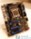
Here are the first pictures of Intel's new high-end CPU socket, the 2011-pin land grid array (LGA2011). A selection of pictures of an unannounced motherboard by MSI made it to the internet. LGA2011, coupled with a new chipset, the Intel X68 Express, will drive the company's new high-end and enthusiast-grade processors that feature 6, 8, or 12 cores, and quad-channel DDR3 memory controllers. At first sight, the LGA2011 is huge! Its retention clip looks to be completely detachable by unhooking the retention bars on either sides. With all LGA sockets till date, you needed to unhook one retention bar, letting you open the retention clip along a hinge.

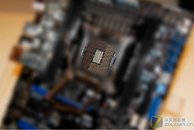
Since the processor has four DDR3 memory channels, there's room for only one DIMM per channel on a typically-sized ATX motherboard. On this particular motherboard, we can make out that there are two DIMM slots on either sides of the socket, accommodating two channels each. With this platform, Intel transferred the northbridge component completely to the CPU package, much like LGA1156/LGA1155. Therefore, the 32-lane PCI-Express controller is housed inside the CPU package. What remains of the chipset is a PCH (platform controller hub). Like P55/H55/P67/H67, the X68 is a PCH, a glorified southbridge. It will house a smaller PCI-E hub that handles various connectivity devices, a storage controller, a LPCIO controller, USB and HDA controllers, and the DMI link to the processor. We will get to know more about this platform as the year progresses.


View at TechPowerUp Main Site
 
So 4 ram slots? Good, was worried I wouldn't be able to get two more matching sets (my ram is EOL) by the time 2011 comes out.
 
That's a pretty weird way to do the RAM slots, doing | | o | | instead of o |||| ( o is the socket and | is a RAM slot).
 
quad-channel DDR3? cool :D
 
Oh cool, so if I were ever to upgrade to this I would only need another kit of RAM, to make 8GB. Sweet!
 
ok i just want to know are them wrong or i am wrong, as i know can't quad channel be useful with 64 bit processors????
 
That's a pretty weird way to do the RAM slots, doing | | o | | instead of o |||| ( o is the socket and | is a RAM slot).

That actually not true at all.

The only reason we saw o |||| is because it was actually like this:

o - N - |||| where N is the northbridge (the memory controller).

Now that N is incorporated onto the CPU die, we can do o - |||| or || - o - ||

Now which one of the above has the shortest distance to the CPU and which one has the most consistent trace lengths? Remember that at high speeds you get all kinds of signalling problems if one memory is twice the distance from the CPU as the other. Inconsistent resistance, capacitance and crosstalk.

The second point is the internal structure of the new multi-core CPU and the internal QPI. You need to think of the memory layout as || - X - || where X is the multicore CPU, and one bank of memory is "closer" to one core and the other bank memory is closer to the other core. And the QPI deals with passing memory data from one side of the CPU to the other if necessary.
 
Last edited:
So 4 ram slots? Good, was worried I wouldn't be able to get two more matching sets (my ram is EOL) by the time 2011 comes out.

how can you make out that the board has 4 memory slots in thos blurry photos?
 
That actually not true at all.

The only reason we saw o |||| is because it was actually like this:

o - N - |||| where N is the northbridge (the memory controller).

Now that N is incorporated onto the CPU die, we can do o - |||| or || - o - ||

Now which one of the above has the shortest distance to the CPU and which one has the most consistent trace lengths? Remember that at high speeds you get all kinds of signalling problems if one memory is twice the distance from the CPU as the other. Inconsistent resistance, capacitance and crosstalk.

The second point is the internal structure of the new multi-core CPU and the internal QPI. You need to think of the memory layout as || - X - || where X is the multicore CPU, and one bank of memory is "closer" to one core and the other bank memory is closer to the other core. And the QPI deals with passing memory data from one side of the CPU to the other if necessary.

I just meant it's different than what I'm used to, but thanks for the informative post. :toast:
 
ok i just want to know are them wrong or i am wrong, as i know can't quad channel be useful with 64 bit processors????

If you had one core, reading a single 64-bit value, with no prefetch and no cache, you might have had a very tentative point. With several cores per chip, relatively large cache line sizes and memory prefetch having quad-channel memory can be quite the help. Of course - the gains won't be all that big for run-of-the-mill apps (just like triple-channel didn't make dual-channel seem slow or obsolete), but they will be there for those who need them and can take advantage of them.
 
how can you make out that the board has 4 memory slots in thos blurry photos?

Xray vision. I see through your photoshopz
 
In the last pic if you look at the top RAM module holders, you can see 4 white blurs.
 
There's good chance these photos are fake. I don't trust any chinese bullshit anyway.
 
If you had one core, reading a single 64-bit value, with no prefetch and no cache, you might have had a very tentative point. With several cores per chip, relatively large cache line sizes and memory prefetch having quad-channel memory can be quite the help. Of course - the gains won't be all that big for run-of-the-mill apps (just like triple-channel didn't make dual-channel seem slow or obsolete), but they will be there for those who need them and can take advantage of them.

as u say cuz i didn't see the tri channel fully use yet, so the quad channel will be useful with 12 cores maybe??
 
as u say cuz i didn't see the tri channel fully use yet, so the quad channel will be useful with 12 cores maybe??

Triple channel is being used beautifully by server applications, which is where it belongs anyway. Same goes for Quad channel memory. They end up in enthusiast systems simply because they share a CPU-design with the server systems and they do make a small impact which the enthusiast crowd is automatically drawn to.
 
I believe there is 2 retention clips because the socket is big but mainly because of memory detection issues on socket 1366 boards.
 
Quad channel...
Just to add a bit more here. This isn't really "quad-channel" but rather it is a dual dual-channel. There are two independent sets of dual-channel memory feeding different cores. There is an internal ring-bus for forwarding memory data in the CPU to the relevant core.

Quad-channel would be better (simpler design) in a single core system.

Dual dual-channel is better (faster) in a multi-core situation where multiple cores are working independently.

[The theoretic bandwidth of the memory is the same, but dual dual-channels can be accessing different memory locations and forwarding the data directly to different processor cores simultaneously and independently. Whereas with quad channel, latency increases when the second memory request from the second core waits for the first to be completed then forwarded by the ring bus.] *

* I put that in brackets because I'm not 100% sure of the implementation in Sandy Bridge. It might use a mixed methodology, ie. using both approaches, depending on demand. We need to know more about how those cache controllers are memory controllers have been designed.
 
Forget the RAM think about the CPU socket, looks huge really.
 
Just curious, how much better is this X68 over P67 chipset. Need a comparison....
 
I know why they blurred it out (to prevent too much info getting leaked), but why not just crop it down to what needs to be looked at? All they have done is made people speculate about the memory. I don't give a **** about the memory. I am on a Bloomfield Core i7 and I am STILL on dual channel and not once have I been begging for more bandwidth. I know there are people who care, but let's not talk about that. I want to see the CPU for cripes sake! That's the real hero here, not some piece of pre-release PCB.

Just curious, how much better is this X68 over P67 chipset. Need a comparison....

My suspicions are not by much. I'd suspect it would maybe have more SATA/USB and a slightly faster PCI-e bus, but I doubt it'll wipe the floor with P67. I am willing to bet they will be interchangeable if someone was nutty enough (not pin for pin, but someone could be crazy enough to make LGA2011 work on P67). Just a guess anyways.
 
That actually not true at all.

The only reason we saw o |||| is because it was actually like this:

o - N - |||| where N is the northbridge (the memory controller).

Now that N is incorporated onto the CPU die, we can do o - |||| or || - o - ||

Now which one of the above has the shortest distance to the CPU and which one has the most consistent trace lengths? Remember that at high speeds you get all kinds of signalling problems if one memory is twice the distance from the CPU as the other. Inconsistent resistance, capacitance and crosstalk.

The second point is the internal structure of the new multi-core CPU and the internal QPI. You need to think of the memory layout as || - X - || where X is the multicore CPU, and one bank of memory is "closer" to one core and the other bank memory is closer to the other core. And the QPI deals with passing memory data from one side of the CPU to the other if necessary.

If that's the reasoning I wonder why this arrangement wasn't used on SB motherboards or even Lynnfield boards where the NB is already integrated? Or is it because those are dual channel boards?

Id like to hear more about these boards, officially anyway.
 
maybe they should make it like this instead
._
|o|
 
Being released in the year 2011. Does Intel have that much time on there hands that they can engineer a socket to have a desirable number of pins, rather than a number that is convenient and works for the technology? Or is it simple coincidence?
 
Back
Top