• Welcome to TechPowerUp Forums, Guest! Please check out our forum guidelines for info related to our community.

NVIDIA GM107 "Maxwell" Silicon Pictured

btarunr

Editor & Senior Moderator
Staff member
Joined
Oct 9, 2007
Messages
47,670 (7.43/day)
Location
Dublin, Ireland
System Name RBMK-1000
Processor AMD Ryzen 7 5700G
Motherboard Gigabyte B550 AORUS Elite V2
Cooling DeepCool Gammax L240 V2
Memory 2x 16GB DDR4-3200
Video Card(s) Galax RTX 4070 Ti EX
Storage Samsung 990 1TB
Display(s) BenQ 1440p 60 Hz 27-inch
Case Corsair Carbide 100R
Audio Device(s) ASUS SupremeFX S1220A
Power Supply Cooler Master MWE Gold 650W
Mouse ASUS ROG Strix Impact
Keyboard Gamdias Hermes E2
Software Windows 11 Pro
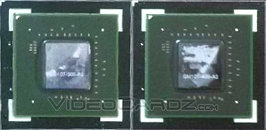
Here is the first picture of a couple of NVIDIA GM107 silicons in a tray, ahead of graphics card assembly. The packages appear to be as big as those of the GK106 from the previous generation, however, the die itself is estimated to be smaller, at roughly 156 mm², compared to the 221 mm² die of the GK106, and the 118 mm² of the GK107. The best part? All three chips are built on the same 28 nm silicon fab process. So what makes the GM107 die smaller than that of the GK106 despite having a similar feature-set? Narrower memory bus. The GM107 is said to feature a 128-bit wide GDDR5 memory interface, in comparison to the 192-bit wide interface of the GK106.

Apart from the 128-bit wide GDDR5 memory interface, the GM107 is said to feature a total of 960 CUDA cores, 80 TMUs, and 16 ROPs. The CUDA core count is identical to that of the GK106. The GM107 is built on NVIDIA's next-generation "Maxwell" GPU architecture. It will form the foundation of two SKUs, the GeForce GTX 750 Ti, and the GeForce GTX 750. The former features the full complement of 960 CUDA cores; while the latter is slightly cut down, and features just 768. The TDP of the GTX 750 Ti is approximated to be around 75 Watt. If true, the GTX 750 duo will set new standards on the performance-per-Watt metrics. NVIDIA is expected to launch both, later this month.


View at TechPowerUp Main Site
 
So doing the same for less? So little maxwell is just really really efficient kepler.
 
960 cores, over 1GHz gpu speed, 28nm for only 75W? If this is true then Nvidia did a little miracle here with Maxwell. The funny thing is that, if 75Ws are true, there is no reason for someone to buy a hi end card today. Either an AMD one or an Nvidia one. Even 790 or the new Titan will be old news before we even see a review of them. 6-9 months life at best for any card over $500 before it is obsolete. Because think Maxwell at 20nm.
 
960 cores, over 1GHz gpu speed, 28nm for only 75W? If this is true then Nvidia did a little miracle here with Maxwell.


75W is good for laptops too. What was the power consumption for a similar performance Kepler card?
 
75W is good for laptops too. What was the power consumption for a similar performance Kepler card?
Between 114Ws (GTX 650ti - 768cores, 128bit, 928MHz) and 140Ws (GTX 660 - 960cores, 192bit, 980Mhz), I think closer to that 140W.
Looking at 700 series, GTX 760 is at 170W with "only" 192 more cores, 256bit data bus and 980MHz gpu speed.
 
So doing the same for less? So little maxwell is just really really efficient kepler.

It's definitely more power efficient. The specs they give for the GK106 are from the 660. From the leaked benchmarks it doesn't compete with it rather the 650 Ti

82a.jpg


75W is good for laptops too. What was the power consumption for a similar performance Kepler card?

110w or 134w depending where it performs

VideoCardz said:
The footprint on power consumption will be dramatically lower than any Kepler GPU. In fact, most GeForce GTX 750 series cards will not require any power connectors, but of course there some with 6-pin installed.

Need more clarity on this. Reference design might not need a 6-Pin but AIBs will have them ?
 
75W at this performance makes its really worthy and easy to put 2 of those on the same PCB, unless its not cost effective because it can be overpriced... we are talking about nvidia here.
 
75W at this performance makes its really worthy and easy to put 2 of those on the same PCB, unless its not cost effective because it can be overpriced... we are talking about nvidia here.

The problem with the two cards idea is that Nvidia cut out the SLi support in the cheaper cards. Don't expect SLi support with these cards.
Didn't read correctly the part about "same PCB". I don't expect something like that anyway.
 
The problem with the two cards idea is that Nvidia cut out the SLi support in the cheaper cards. Don't expect SLi support with these cards.
Didn't read correctly the part about "same PCB". I don't expect something like that anyway.
Asus put two mid range GTX760 cores on the same PCB, so I was thinking they might do it again with these but at a very convenient price, and not $600+.
 
Asus put two mid range GTX760 cores on the same PCB, so I was thinking they might do it again with these but at a very convenient price, and not $600+.

Yes I realized what you where saying but, later, after posting. The problem with 750 is that it wouldn't support(I guess) SLi, so, is it possible to put two gpus that they possibly don't support SLi on the same PCB?
The fact that a card like this might cost about $250, maybe it wouldn't make it financially viable. Also it doesn't offer much as a publicity stunt. ASUS's card was fast enough to be advertised as "faster than Titan" this might be faster than 760 and with less power consumption, but not something that someone would be interested in buying. A single gpu is always preferable.
 
I can see clearly now that these GPUs are made for incoming slew of steam machines running on cheap TFX 150W PSUs
 
Need more clarity on this. Reference design might not need a 6-Pin but AIBs will have them ?

Being 75 watts is all PCI-e provides. would be a 6pin pci-e for it cause boost clock will put it over 75.
 
That new die size is much better suited to have ROI than the GK106 ever was for them! The 750 will be the 75W part, while the 750Ti could be as high as 110W.

So slighty smaller than the Bonaire XTX, with it's 115W TDP, and by the Fire Strike above much like a reference R7 260X.
 
Last edited:
82a.jpg


Look at that valley score, this will compete with 7790 and maybe 260x at best.
 
Valley is the worst one by a long shot. The above scores vary 70-96% of the GTX 660. I'm guessing with real games with usable settings, it does better than what the Valley benchmark suggests. Push it, and 2/3 ROPs and 2/3 vram width shine through with a 70% result.
 
That new die size is much better suited to have ROI than the GK106 ever was for them! The 750 will be the 75W part, while the 750Ti could be as high as 110W.

FFS, how about dialling down the FUD for a change.
From the Videocardz link bta linked to, it clearly shows that the fully enabled (960 shader) die is ~75W. You also posted on the previous article where the original SweClockers link bta provided clearly stated:
Both graphics cards will also be without connections to external power supply , which ensures a maximum TDP of 75 watts.
Yet you still persist is attributing your own arbitrary numbers
Given these numbers unless they are on a <160mm2 dia, while staying under 110W TDP they aren't going to be much if any influence.
All this, when every source seems to note that the cards leaked are overclocked SKUs, and still don't utilise anything other than the PCI-E slot for power.
:banghead:
 
Last edited:
All this, when every source seems to note that the cards leaked are overclocked SKUs, and still don't utilise anything other than the PCI-E slot for power.
Don't get that Chef's hat in such a wad.

I'm just reading the information as provided from both the TPU articles, and there’s always someone here to provide a alternate opinion. I'm not the only one on this thread that's skeptical of a Ti OC not needing the 6-Pin.

First, that “other” TPU article never mentions the TDP for either. I don't read Swedish and won't normally have time to translate every article, it's a shame that information was omitted within btarunrs’ re-write, take that up with him. If you look I wrote that several hour before the post here.

While yes I just miss-read it denoting the "Ti" designation; "The TDP of the GTX 750 Ti is approximated to be around 75 Watt". With all the designators Ti /non-Ti and former/latter bantered-about I just took away the wrong information, a simple mistake. While are you saying even the OC'd (and are you indicating Ti's) don't utilize anything other than the PCI-E slot power?

I'll hold to a wait and see as we know much of this communication get convoluted and mixed-up just as I have.
 
Last edited:
First, that “other” TPU article never mentions the TDP for either.
Might I suggest you actually read the source material - the original article links are provided for a reason....assuming you're actually interested of course
I don't read Swedish and won't normally have time to translate every article it's a shame that information was omitted within btarunrs’ re-write, take that up with him.
Why? My schedule allowed for 75 seconds to translate the SweClockers article link that bta provided. I honestly didn't realise that Google translate, or copy/pasting a block of text into any other online translator was deemed such a time consuming business. Your life must be phenomenally busy, although I wonder how you couldn't budget a couple of minutes to translate and read a paragraph of source material, but could find the time to reply to my post
If you look I wrote that several hour before the post here.
Which makes the post here all the more suspect, considering the article (and the SweClockers link provided) you earlier posted on had all the relevant information to hand.
While yes I just miss-read it denoting the "Ti" designation; "The TDP of the GTX 750 Ti is approximated to be around 75 Watt".
The likely reason it is approximated is if the card does not a PCI-E power input, the cards draw is limited to a nominal 75W through the PCI-E x16 slot.
While are you saying even the OC'd (and are you indicating Ti's) don't utilize anything other than the PCI-E slot power?
What I'm seeing is a low-end priced card with a 75W power budget with clocks of 1085MHz core/1163MHz boost. Now, there may well be SKUs with an auxiliary 6-pin power input...so what kind of clocks do you think are attainable by substantially increasing input power? Do you not think that a board with a 150W board power budget might conceivably offer more performance than the 75W board tested in the article? Yet you ascribe the higher power budget of a so-far unidentified board with the performance of a tested board using ≤75W. Doesn't seem very logical or likely IMO, and nor does pushing the clock frequencies past what are already substantial numbers for an entry level model....are we in an era where 1200-1300MHz in the sub-$150 segment is going to be the norm? If so, then Nvidia have done wonders tweaking a Kepler design still on 28nm. Kind of makes you wonder why their competitor seems stalled at the 1GHz mark, no?
 
Last edited:
One of the first leaks and listing from Tmall made reference to a 6-pin

GeForce-GTX-750-GPU-Picture.png


I can't translate that but its clear 6pin is there and its referring to the 768 core variant.
 
Last edited:
One of the first leaks and listing from Tmall made reference to a 6-pin
I saw that a couple of days ago along with a pre-order for an Asus GTX 750 Ti, which also stated that the 1033/1098 were reference clock speeds, and that the card was a 140W part...which makes it slower, more power hungry, and more expensive than the part it is designed to replace. Something doesn't add up.
 
To me it looks like a refresh rather then what "Maxwell" is suppose to be.

GK107 was a 75w(-)

GM107 reference or not 750/750 Ti is looking like a GK106 75w(+). It also might be there able to stretch out a bit more on a smaller die to sell smaller dies at a higher margin.

Nvidia could just paper launch a reference card that doesn't need a 6pin and let the partners add a 6pin. Nvidia can say it doesn't need one but the partners added.
 
Last edited:
Something doesn't add up.
Exactly, they are still on 28Nm and effectively shrank the die by clipping the memory bus, and other changes. But still being 960 Cuda part I can't see some 50% improvement on efficiency, all while higher clocks… on 20Nm perhaps. If they can find a 20% improvement for a 960 Cuda part they'll be doing great. While the 768 Cuda part on GK106 was 110W, I’ve no issue saying they can get it to be 75W.

If wrong and they're better... all the better, but given the information we have to scrutinize it seems to be shaping up as such. Holding to 28Nm is probably one of the biggest limiting issues to the efficiency. Maxwell it's self is evolutionary; it's 20Nm/Denver/UVM that will make it revolutionary.
 
I agree.

The only Kepler cards that didn't require a 6-pin connector where all 384 cores or less and didn't have boost clocks.
 
Last edited:
Back
Top