• Welcome to TechPowerUp Forums, Guest! Please check out our forum guidelines for info related to our community.

NVIDIA Wants 450 mm Wafers, Seeking Foundry Partnership with GlobalFoundries, Samsung

btarunr

Editor & Senior Moderator
Staff member
Joined
Oct 9, 2007
Messages
47,670 (7.43/day)
Location
Dublin, Ireland
System Name RBMK-1000
Processor AMD Ryzen 7 5700G
Motherboard Gigabyte B550 AORUS Elite V2
Cooling DeepCool Gammax L240 V2
Memory 2x 16GB DDR4-3200
Video Card(s) Galax RTX 4070 Ti EX
Storage Samsung 990 1TB
Display(s) BenQ 1440p 60 Hz 27-inch
Case Corsair Carbide 100R
Audio Device(s) ASUS SupremeFX S1220A
Power Supply Cooler Master MWE Gold 650W
Mouse ASUS ROG Strix Impact
Keyboard Gamdias Hermes E2
Software Windows 11 Pro
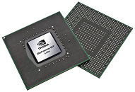
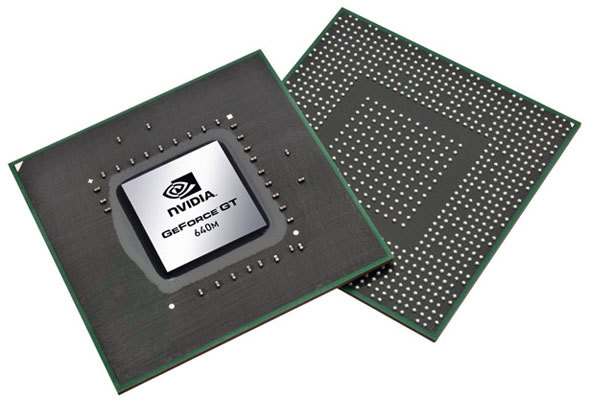
NVIDIA is formulating a long-term chip manufacturing strategy that will see its interests secure by the time chip manufacturing has moved on to 14 nm (which follows 20 nm and today's 28 nm), which could arrive around 2015. Chip manufacturing by foundry partners is a potentially major irritant for NVIDIA, which wants to see wafer sizes getting increased from the current 300 mm manufacturing at TSMC, to 450 mm, and fast. TSMC will achieve 450 mm (18-inch) wafer manufacturing capability only by 2015. Another irritant for NVIDIA is TSMC's change in business model, which charges fabless customers "per wafer manufactured", rather than "per working chip yielded", giving them what they perceive to be the shorter end of the stick. NVIDIA is thus rigorously evaluating other foundry partners. We know from a slightly older report that Samsung has sent NVIDIA test chips manufactured at its Austin, Texas facility. There is talk that NVIDIA could also seek partnerships with GlobalFoundries, of which AMD recently relinquished all its stakes on. NVIDIA needs reliable, high-volume foundry partners that can keep it competitive not just with its main business of GPUs, but also a potential gold mine that is application processors.


View at TechPowerUp Main Site
 
Does anyw\one even have a 450mm Fab? As far as I know they still have a lot of problems with 450mm manufacturing.
 
I don't know, but something needs to be done so that nvidia can have a healthy stock of gtx680 on retail shelves!
 
I not 100% certain but I don't think this is some sudden "TSMC's change in business model"... It's standard practice for foundries to decide how to charge, per wafer or per working chip, when they sign a contract. It's a balancing act based on yield expectations.

nV had a splendid per-chip deal that let them sail through Fermi times. Now that the old contract is over TSMS wants to make some of it's money back. It's natural for nV to want larger wafers in this case.
 
Yep Nvidia had/only got that option from TSMC this time around to buy full wafers. TSMC supplies them 28Nm HP HkMG wafers at a newer higher price, and then it's up to the buyer (Nvidia and AMD) to hunt out the good ones.

It's a here's your wafer, if you find bushels of lemons it's your problem. TSMC is not affected by Nvidia choosing to run with their HP HkMG process to grab the theoretical clock/efficiency touted by the new gate design. I think Nvidia got snookered one to many times by TSMC.

AMD kept with the more traditional 28Nm LP process, and their normal price per wafer, although they got the same 28Nm price hike. AMD now since TSMC stopped to fix the production problems are delivering decent yields, so now AMD can reflect that in their pricing.
 
If you read the financial conference call for nVidia, they said that they changed from per die to per wafer back when Fermi first came out. This isn't something "new" as the nVidia PR department is trying to spin it as.
 
Go FOR Samsung !

Samsung Can Do Miracles !
 
you cant barking on someone to do something that their still incapable to achieve it. patience is a lesson, you name it..
 
Back
Top