T0@st
News Editor
- Joined
- Mar 7, 2023
- Messages
- 2,952 (3.82/day)
- Location
- South East, UK
| System Name | The TPU Typewriter |
|---|---|
| Processor | AMD Ryzen 5 5600 (non-X) |
| Motherboard | GIGABYTE B550M DS3H Micro ATX |
| Cooling | DeepCool AS500 |
| Memory | Kingston Fury Renegade RGB 32 GB (2 x 16 GB) DDR4-3600 CL16 |
| Video Card(s) | PowerColor Radeon RX 7800 XT 16 GB Hellhound OC |
| Storage | Samsung 980 Pro 1 TB M.2-2280 PCIe 4.0 X4 NVME SSD |
| Display(s) | Lenovo Legion Y27q-20 27" QHD IPS monitor |
| Case | GameMax Spark M-ATX (re-badged Jonsbo D30) |
| Audio Device(s) | FiiO K7 Desktop DAC/Amp + Philips Fidelio X3 headphones, or ARTTI T10 Planar IEMs |
| Power Supply | ADATA XPG CORE Reactor 650 W 80+ Gold ATX |
| Mouse | Roccat Kone Pro Air |
| Keyboard | Cooler Master MasterKeys Pro L |
| Software | Windows 10 64-bit Home Edition |
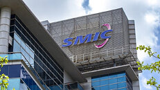
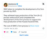
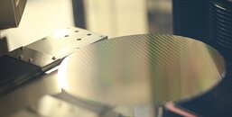
According to a report produced by semiconductor industry analysts at Kiwoom Securities—a South Korean financial services firm—Semiconductor Manufacturing International Corporation (SMIC) is expected to complete the development of a 5 nm process at some point in 2025. Jukanlosreve summarized this projection in a recent social media post. SMIC is often considered to be China's flagship foundry business; the partially state-owned organization seems to heavily involved in the production of (rumored) next-gen Huawei Ascend 910 AI accelerators. SMIC foundry employees have reportedly struggled to break beyond a 7 nm manufacturing barrier, due to lack of readily accessible cutting-edge EUV equipment. As covered on TechPowerUp last month, leading lights within China's semiconductor industry are (allegedly) developing lithography solutions for cutting-edge 5 nm and 3 nm wafer production.
Huawei is reportedly evaluating an in-house developed laser-induced discharge plasma (LDP)-based machine, but finalized equipment will not be ready until 2026—at least for mass production purposes. Jukanlosreve's short interpretation of Kiwoom's report reads as follows: (SMIC) achieved mass production of the 7 nm (N+2) process without EUV and completed the development of the 5 nm process to support the mass production of the Huawei Ascend 910C. The cost of SMIC's 5 nm process is 40-50% higher than TSMC's, and its yield is roughly one-third." The nation's foundries are reliant on older ASML equipment, thus are unable to produce products that can compete with the advanced (volume and quality) output of "global" TSMC and Samsung chip manufacturing facilities. The fresh unveiling of SiCarrier's Color Mountain series has signalled a promising new era for China's foundry industry.
View at TechPowerUp Main Site | Source
Huawei is reportedly evaluating an in-house developed laser-induced discharge plasma (LDP)-based machine, but finalized equipment will not be ready until 2026—at least for mass production purposes. Jukanlosreve's short interpretation of Kiwoom's report reads as follows: (SMIC) achieved mass production of the 7 nm (N+2) process without EUV and completed the development of the 5 nm process to support the mass production of the Huawei Ascend 910C. The cost of SMIC's 5 nm process is 40-50% higher than TSMC's, and its yield is roughly one-third." The nation's foundries are reliant on older ASML equipment, thus are unable to produce products that can compete with the advanced (volume and quality) output of "global" TSMC and Samsung chip manufacturing facilities. The fresh unveiling of SiCarrier's Color Mountain series has signalled a promising new era for China's foundry industry.


View at TechPowerUp Main Site | Source


