• Welcome to TechPowerUp Forums, Guest! Please check out our forum guidelines for info related to our community.

TSMC 7nm EUV Process to Enter Mass-Production in March 2019

btarunr

Editor & Senior Moderator
Staff member
Joined
Oct 9, 2007
Messages
47,670 (7.43/day)
Location
Dublin, Ireland
System Name RBMK-1000
Processor AMD Ryzen 7 5700G
Motherboard Gigabyte B550 AORUS Elite V2
Cooling DeepCool Gammax L240 V2
Memory 2x 16GB DDR4-3200
Video Card(s) Galax RTX 4070 Ti EX
Storage Samsung 990 1TB
Display(s) BenQ 1440p 60 Hz 27-inch
Case Corsair Carbide 100R
Audio Device(s) ASUS SupremeFX S1220A
Power Supply Cooler Master MWE Gold 650W
Mouse ASUS ROG Strix Impact
Keyboard Gamdias Hermes E2
Software Windows 11 Pro
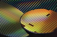
TSMC is giving final touches to set its flagship 7 nanometer EUV (extreme ultraviolet lithography) silicon fabrication node at its highest state of readiness for business, called mass-production. At this state, the node can mass-produce products for TSMC's customers. TSMC had taped out its first 7 nm EUV chips in October 2018. The company will also begin risk-production of the more advanced 5 nm node in April, staying on schedule. Mass production of 5 nm chips could commence in the first half of 2020.

The 7 nm EUV node augments TSMC's 7 nm DUV (deep ultraviolet lithography) node that's been already active since April 2018, and producing chips for AMD, Apple, HiSilicon, and Xilinx. At the turn of the year, 7 nm DUV made up 9 percent of TSMC's shipments. With the new node going online, 7 nm (DUV + EUV) could make up 25 percent of TSMC's output by the end of 2019.


View at TechPowerUp Main Site
 
Are 7nm duv designs super easy to port to 7nm euv? I mean like copy paste like going from 14nm gf to 12nm gf. That way existing designs can be transferred with minimal redesign? Maybe Zen2+
 
Are 7nm duv designs super easy to port to 7nm euv? I mean like copy paste like going from 14nm gf to 12nm gf. That way existing designs can be transferred with minimal redesign? Maybe Zen2+
That depends on too many things to answer easily. For example if the cleanliness of the channel/pitch isn't maintained they may have to increase distance between them, or the depth may be different. It's usually a couple respins to get it right.
 
Is this means Navi will be using 7nm EUV??
 
EUV is single-patterned, DUV is multi-patterned

EUV exposure is done by a small "blast" (complicated plasma stuff) that creates a burst of rays and guides the rays through complicated means (not lens) to in the right shape for exposure.
DUV still works with lens made from exotic materials (but traditional patterning)

Totally not compatible, but since these have been in the works for many years already, no surprise that it's now finally read for mass production.
 
Is this means Navi will be using 7nm EUV??
Yes. Because an announcement about TSMC is all about AMD.
Also, did you read the "Mass production of 5 nm chips could commence in the first half of 2020" part?
 
EUV exposure is done by a small "blast" (complicated plasma stuff)
Not so complicated. :-)
You take some matter, you heat it up and it starts to emit energy in different forms. Tin used in this process emits EUV.
that creates a burst of rays and guides the rays through complicated means (not lens) to in the right shape for exposure.
Again: not that hard to understand. I assume most of us have seen a concave mirror and know from experience that it can be used to focus light. :-)

Problem with Extreme UV (few times shorter wavelength compared to UV in "DUV") is that it's easily absorbed by matter. The whole EUV process takes place in very high vacuum and it would be hard to make a lens that works in this setup - even a gas one (it would absorb too much).
But it is possible to replace a lens with a set of curved mirrors.

Sadly, no magic. :-)
 
Yes. Because an announcement about TSMC is all about AMD.
Also, did you read the "Mass production of 5 nm chips could commence in the first half of 2020" part?
The reason I asked as Navi delyed(by rumor) for 3rd quater. And Apple,Mediatek, Qualcomm don't enterest me wheather they use 5nm or 3nm.
And beside AMD (and those monbile phone makers) who is using TSMC's 7nm?? Nvidia??
 
Is this means Navi will be using 7nm EUV??

Chip design and node go hand in hand, you can't stop mid way and change one of them. Navi wont be using EUV, not now.
 
Last edited:
The reason I asked as Navi delyed(by rumor) for 3rd quater. And Apple,Mediatek, Qualcomm don't enterest me wheather they use 5nm or 3nm.
And beside AMD (and those monbile phone makers) who is using TSMC's 7nm?? Nvidia??
Huawei, Nvidia, maybe Intel. Possibly few more.

Also do consider that Apple is rumored to be working on in-house CPU and GPU. They have 10-15% market share in personal computers. Basically, if they really wanted, they could use all TSMC 7nm potential for the next few years. :-)
 
Huawei, Nvidia, maybe Intel. Possibly few more.

Also do consider that Apple is rumored to be working on in-house CPU and GPU. They have 10-15% market share in personal computers. Basically, if they really wanted, they could use all TSMC 7nm potential for the next few years. :)
Apple is now a bit less than 7%, around Acer levels.
 
Is this means Navi will be using 7nm EUV??
No. It means nothing for AMD. If Navi turns out to be a mid tier part like it’s rumored to be, it may end up being 12nm to reduce cost. At this point 7nm is too expensive to just use on whatever.
 
No. It means nothing for AMD. If Navi turns out to be a mid tier part like it’s rumored to be, it may end up being 12nm to reduce cost. At this point 7nm is too expensive to just use on whatever.

Navi is 7nm. Has been since the start and even labeled on their roadmap as 7nm. They are not going to port it back to 12nm at this point. That would put it in 2020 lol.
 
No. It means nothing for AMD. If Navi turns out to be a mid tier part like it’s rumored to be, it may end up being 12nm to reduce cost. At this point 7nm is too expensive to just use on whatever.
Actually it's the opposite. :)
"Mid-tier" is what actually matters. A good 7nm process will improve power efficiency and reduce size. That's what AMD needs to make Navi successful.
At first 7nm supply will be very limited, so AMD will use it for the mainstream products. The less important high-end parts will have to wait (or AMD may not make them at all).

Console makers' patience is limited, but they are staying with AMD for next gen.
AMD must have promised them them a huge improvement in efficiency...
 
Last edited:
In its current 7nm offering AMD provides only 2x density which is close to 60% now because 13,230 million /331 is ~40, and 12,500 million /495 in VEGA10 is ~25. And all that for 250 Mhz 16% boost at same TDP that pulls ahead only by 25%, the effect of having +110% memory bandwidth no less. So much for efficiency. ZEN2 will atleast remove the bottleneck in consoles.

7nm EUV should provide ~~ density of 100 or 4x that of 14nm.
 
At first 7nm supply will be very limited, so AMD will use it for the mainstream products.

Really?
That doesn't make sense even without me pointing out that Vega 20 is a 7nm part while mainstream parts are not.
 
Really?
That doesn't make sense even without me pointing out that Vega 20 is a 7nm part while mainstream parts are not.
Vega 20 is the first consumer Radeon released since AMD got their hands on 7nm.

And what doesn't make sense? AMD makes GPUs that aren't even close to what next gen consoles are supposed to be. That's the demand they have to protect.
The battle in high-end PC gaming is lost at this point. They may try again (and they should), but only after they secure some sensible cashflow. You know... in case Nvidia makes a better GPU anyway and AMD has to file for bankruptcy. Makes sense now?
 
No. It means nothing for AMD. If Navi turns out to be a mid tier part like it’s rumored to be, it may end up being 12nm to reduce cost. At this point 7nm is too expensive to just use on whatever.
It appears GF/AMD WSA gives AMD really good rates on GF wafers. That is probably part of why GF 7nm would never economically make sense. From what little we could tell, GF was always losing money on AMD's price-negotiated wafers, anyways (mostly due to GF incompetence, since they have basically screwed up every process they made from 32nm onwards - 32nm being the first process they made since being spun off from AMD).
 
Back
Top