- Joined
- Aug 19, 2017
- Messages
- 2,999 (1.06/day)
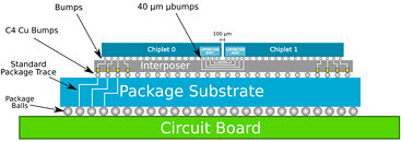
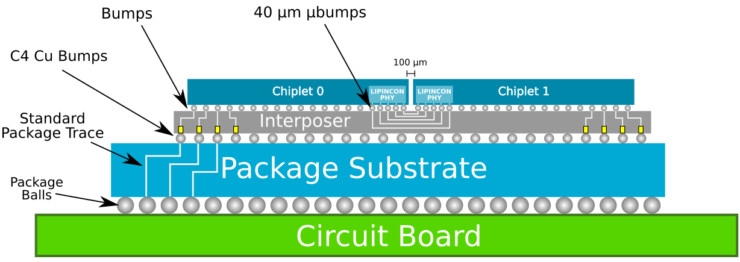
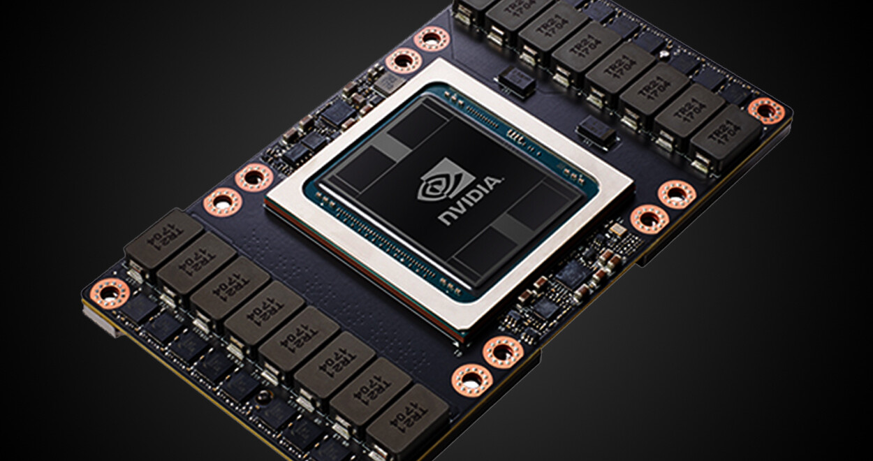
TSMC, Taiwan's flagship manufacturer of silicon, has seen a substantial increase in demand for Chip-on-Wafer-on-Substrate (CoWoS) packaging technology, according to the report from DigiTimes. CoWoS is a multi-chip packaging technology that gives an option to build silicon like LEGO, allowing for dies to be placed side by side on interposer that is providing high interconnect density and performance. You can see more about CoWoS in detail here. Some of the examples of CoWoS are NVIDIA's P100 and V100 dies that integrate logic (computing elements), and memory (in the form of HBM) on a single die.
Recently, TSMC updated its CoWoS technology, where this new second-generation parts could scale far larger than the first-generation implementation - up to 1700 squared millimeters of die space, allowing for some very creative solutions to be implemented. This may be the reason that the demand in Q2 has risen so substantially and that TSMC's production lines are now running at full capacity, trying to meet the demand for this packaging technology.
View at TechPowerUp Main Site


