- Joined
- Aug 19, 2017
- Messages
- 2,815 (1.02/day)
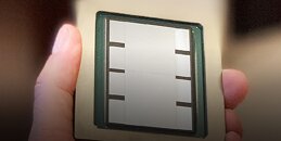
TSMC, the world's leading semiconductor manufacturing company, is rumored to start production of its 6th generation Chip-on-Wafer-on-Substrate (CoWoS) packaging technology. As the silicon scaling is getting ever so challenging, the manufacturers have to come up with a way to get as much performance as possible. That is where TSMC's CoWoS and other chiplet technologies come. They allow designers to integrate many integrated circuits on a single package, making for a cheaper overall product compared to if the product used one big die. So what is so special about 6th generation CoWoS technology from TSMC, you might wonder. The new generation is said to enable a massive 12 stacks of HBM memory on a package. You are reading that right. Imagine if each stack would be an HBM2E variant with 16 GB capacity that would be 192 GB of memory on the package present. Of course, that would be a very expensive chip to manufacture, however, it is just a showcase of what the technology could achieve.
Update 16:44 UTC—The English DigiTimes report indicates that this technology is expected to see mass production in 2023.

View at TechPowerUp Main Site
Update 16:44 UTC—The English DigiTimes report indicates that this technology is expected to see mass production in 2023.

View at TechPowerUp Main Site


