Report an Error


CLEVO GTX 980 Mobile
- Graphics Processor
- GM204
- Cores
- 2048
- TMUs
- 128
- ROPs
- 64
- Memory Size
- 8 GB
- Memory Type
- GDDR5
- Bus Width
- 256 bit

GPU

Back
Graphics Processor
- GPU Name
- GM204
- GPU Variant
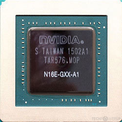
- N16E-GXX-A1
- Architecture
- Maxwell 2.0
- Foundry
- TSMC
- Process Size
- 28 nm
- Transistors
- 5,200 million
- Density
- 13.1M / mm²
- Die Size
- 398 mm²
- Chip Package
- BGA-1745
Mobile Graphics
- Release Date
- Sep 21st, 2015
- Generation
- GeForce 900M
- Predecessor
- GeForce 800M
- Successor
- GeForce 10 Mobile
- Production
- End-of-life
- Bus Interface
- MXM-B (3.0)
Clock Speeds
- Base Clock
1064 MHz
1127 MHz (+6%)
- Boost Clock
1140 MHz
1216 MHz (+7%)
- Memory Clock
-
1753 MHz
1503 MHz (-14%)
7 Gbps effective
6 Gbps effective
Memory
- Memory Size
- 8 GB
- Memory Type
- GDDR5
- Memory Bus
- 256 bit
- Bandwidth
-
224.4 GB/s
192.4 GB/s
Render Config
- Shading Units
- 2048
- TMUs
- 128
- ROPs
- 64
- SMM Count
- 16
- L1 Cache
- 48 KB (per SMM)
- L2 Cache
- 2 MB
Theoretical Performance
- Pixel Rate
-
72.96 GPixel/s
77.82 GPixel/s
- Texture Rate
-
145.9 GTexel/s
155.6 GTexel/s
- FP32 (float)
-
4.669 TFLOPS
4.981 TFLOPS
- FP64 (double)
-
145.9 GFLOPS
155.6 GFLOPS (1:32)
Board Design
- Slot Width
- MXM Module
- TDP
- unknown
- Outputs
- Portable Device Dependent
- Power Connectors
- None
Graphics Features
- DirectX
- 12 (12_1)
- OpenGL
- 4.6
- OpenCL
- 3.0
- Vulkan
- 1.3
- CUDA
- 5.2
- Shader Model
- 6.8
GM204 GPU Notes
| NVENC: 5th Gen NVDEC: 1st Gen PureVideo HD: VP6 VDPAU: Feature Set E Latest Drivers: Windows Vista: GeForce Release 365.19 Quadro Release R346 U7 (348.40) / R352 BETA (352.86) Windows 7 / 8 / 8.1 (x32 / x64): GeForce Release 391.35 / 474.89 Quadro Release R390 U9 (392.37) / R440 U4 (441.66) Data Center Release 427.11 Windows 10 / 11 (x32 / x64): GeForce Release 391.35 / Latest Quadro Release R390 U9 (392.37) / Latest Data Center Release: Latest |
Other retail boards based on this design (2)
| Name | GPU Clock | Boost Clock | Memory Clock | Other Changes |
|---|---|---|---|---|
|
CLEVO GTX 980 Mobile

|
1127 MHz | 1216 MHz | 1503 MHz | |
| 1190 MHz | 1291 MHz | 1753 MHz | 4 GB |

Sep 2nd, 2024 22:14 EDT
change timezone
Latest GPU Drivers
New Forum Posts
- Is this where CPUs is the primary focus ? (21)
- Beware! Fake Ryzen 7800X3D CPUs are being sold (37)
- ASUS X99-Deluxe II (4)
- 5800x (and other Zen 3 chips) PBO settings/Temperature fix (966)
- Which is your favourite controller? (51)
- TPU's Nostalgic Hardware Club (18879)
- Underclocking(?) (25)
- Can unplugging the PC repeatedly from the wall harm it? (69)
- DTS DCH Driver for Realtek HDA [DTS:X APO4 + DTS Interactive] (1969)
- 32 inch 240hz 4K oled discussion (including price disparity) (9)
Popular Reviews
- Star Wars Outlaws Handheld Performance Review - Steam Deck and ROG Ally Tested
- Kingston NV3 Review - Much Improved Over NV2
- Star Wars Outlaws Performance Benchmark Review - 35 GPUs Tested
- Star Wars Outlaws: DLSS vs. FSR vs. XeSS Comparison Review
- Black Myth Wukong In-Game Performance Benchmark Review - 35 GPUs Tested
- Black Myth: Wukong Handheld Performance Benchmark Review - Steam Deck and ROG Ally Tested
- Black Myth Wukong: DLSS vs. FSR vs. XeSS Comparison Review
- ASUS GeForce RTX 4090 STRIX OC Review
- MSI GeForce RTX 4090 Gaming X Trio Review
- ASUS GeForce RTX 4090 Matrix Platinum Review - The RTX 4090 Ti
Controversial News Posts
- AnandTech Shuts Down, an Icon of Tech News and Reviews Rides into the Sunset (143)
- Puget Systems Releases CPU Failure Report: AMD CPUs Achieve Higher Failure Rate Than Intel 13th and 14th Generation (127)
- "Sinkclose" Vulnerability Affects Every AMD CPU Dating Back to 2006 (123)
- AMD Ryzen Branch Prediction Optimizations Now Available to Windows 11 23H2 (121)
- Intel Ships 0x129 Microcode Update for 13th and 14th Generation Processors with Stability Issues (119)
- Steam Survey July 2024 Update: Windows 10 Usage Records Uptick, Windows 11 Drops (115)
- AMD Readies Ryzen 5 5500X3D Socket AM4 Processor with 3D V-Cache (109)
- NVIDIA's RTX 5060 "Blackwell" Laptop GPU Comes with 8 GB of GDDR7 Memory Running at 28 Gbps, 25 W Lower TGP (108)