Report an Error


NVIDIA Quadro 400
- Graphics Processor
- GT216
- Cores
- 48
- TMUs
- 16
- ROPs
- 8
- Memory Size
- 512 MB
- Memory Type
- DDR3
- Bus Width
- 64 bit

GPU

I/O

Top

Bottom
Recommended Gaming Resolutions:
- 640x480
- 1280x720
- 1366x768
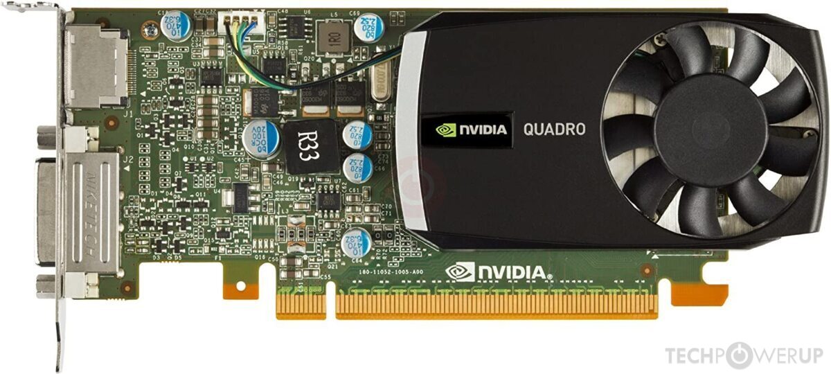
The Quadro 400 was a mid-range professional graphics card by NVIDIA, launched on April 5th, 2011. Built on the 40 nm process, and based on the GT216 graphics processor, in its GT216 GL variant, the card supports DirectX 11.1. Even though it supports DirectX 11, the feature level is only 10_1, which can be problematic with many DirectX 11 & DirectX 12 titles. The GT216 graphics processor is a relatively small chip with a die area of only 100 mm² and 486 million transistors. It features 48 shading units, 16 texture mapping units, and 8 ROPs. NVIDIA has paired 512 MB DDR3 memory with the Quadro 400, which are connected using a 64-bit memory interface. The GPU is operating at a frequency of 450 MHz, memory is running at 770 MHz.
Being a single-slot card, the NVIDIA Quadro 400 does not require any additional power connector, its power draw is rated at 32 W maximum. Display outputs include: 1x DVI, 1x DisplayPort. Quadro 400 is connected to the rest of the system using a PCI-Express 2.0 x16 interface. The card measures 163 mm in length, 69 mm in width, and features a single-slot cooling solution. Its price at launch was 169 US Dollars.
Being a single-slot card, the NVIDIA Quadro 400 does not require any additional power connector, its power draw is rated at 32 W maximum. Display outputs include: 1x DVI, 1x DisplayPort. Quadro 400 is connected to the rest of the system using a PCI-Express 2.0 x16 interface. The card measures 163 mm in length, 69 mm in width, and features a single-slot cooling solution. Its price at launch was 169 US Dollars.
Graphics Processor
Graphics Card
- Release Date
- Apr 5th, 2011
- Generation
-
Quadro Fermi
(x000)
- Predecessor
- Quadro FX Tesla
- Successor
- Quadro Kepler
- Production
- End-of-life
- Launch Price
- 169 USD
- Bus Interface
- PCIe 2.0 x16
- Reviews
- 26 in our database
Relative Performance
Based on TPU review data: "Performance Summary" at 1920x1080, 4K for 2080 Ti and faster.
Performance estimated based on architecture, shader count and clocks.
Clock Speeds
- GPU Clock
- 450 MHz
- Shader Clock
- 1125 MHz
- Memory Clock
-
770 MHz
1540 Mbps effective
Memory
- Memory Size
- 512 MB
- Memory Type
- DDR3
- Memory Bus
- 64 bit
- Bandwidth
- 12.32 GB/s
Render Config
- Shading Units
- 48
- TMUs
- 16
- ROPs
- 8
- SM Count
- 6
- L2 Cache
- 32 KB
Theoretical Performance
- Pixel Rate
- 3.600 GPixel/s
- Texture Rate
- 7.200 GTexel/s
- FP32 (float)
- 108.0 GFLOPS
Board Design
- Slot Width
- Single-slot
- Length
- 163 mm
6.4 inches
- Width
- 69 mm
2.7 inches
- TDP
- 32 W
- Suggested PSU
- 200 W
- Outputs
- 1x DVI
1x DisplayPort
- Power Connectors
- None
- Board Number
- P1052 SKU 500
Graphics Features
- DirectX
- 11.1 (10_1)
- OpenGL
- 3.3
- OpenCL
- 1.1
- Vulkan
- N/A
- CUDA
- 1.2
- Shader Model
- 4.1
GT216 GPU Notes
| PureVideo HD: VP4 VDPAU: Feature Set C Latest Drivers: Windows 2000: Quadro Release 261.19 Windows XP / Server 2003 x64: GeForce Release 185.81 (Notebooks) GeForce Release 340.52 Quadro Release R319 U2 (321.01) Tesla Release 258.96 Windows Vista: GeForce Release 307.83 (Notebooks) GeForce Release 342.01 Quadro Release R340 U15 (342.01) Tesla Release 258.96 Windows 7 / 8 / 8.1 / 10: GeForce Release 342.01 Quadro Release R340 U15 (342.01) Tesla Release 258.96 |
Apr 15th, 2025 03:01 EDT
change timezone
Latest GPU Drivers
New Forum Posts
- TPU's Nostalgic Hardware Club (20243)
- 7800X3D and 5070 Ti / 9070 XT Build (15)
- Weird pc slow down as soon as PCI-E card is in the system (9)
- A dozen drivers for HD4670, and which do I choose? (17)
- best ram to buy for my usage and system specs? (34)
- Gigabyte 9070 XT audio issues (35)
- What's your latest tech purchase? (23555)
- The TPU UK Clubhouse (26089)
- Flash another RTX 4060 vBIOS to get zero rpm fan support (3)
- XFX RX 590 GME china (7)
Popular Reviews
- G.SKILL Trident Z5 NEO RGB DDR5-6000 32 GB CL26 Review - AMD EXPO
- ASUS GeForce RTX 5080 TUF OC Review
- Thermaltake TR100 Review
- The Last Of Us Part 2 Performance Benchmark Review - 30 GPUs Compared
- TerraMaster F8 SSD Plus Review - Compact and quiet
- Zotac GeForce RTX 5070 Ti Amp Extreme Review
- Sapphire Radeon RX 9070 XT Pulse Review
- DAREU A950 Wing Review
- Sapphire Radeon RX 9070 XT Nitro+ Review - Beating NVIDIA
- Upcoming Hardware Launches 2025 (Updated Apr 2025)
Controversial News Posts
- NVIDIA GeForce RTX 5060 Ti 16 GB SKU Likely Launching at $499, According to Supply Chain Leak (182)
- NVIDIA Sends MSRP Numbers to Partners: GeForce RTX 5060 Ti 8 GB at $379, RTX 5060 Ti 16 GB at $429 (124)
- Nintendo Confirms That Switch 2 Joy-Cons Will Not Utilize Hall Effect Stick Technology (105)
- Over 200,000 Sold Radeon RX 9070 and RX 9070 XT GPUs? AMD Says No Number was Given (100)
- Nintendo Switch 2 Launches June 5 at $449.99 with New Hardware and Games (99)
- Sony Increases the PS5 Pricing in EMEA and ANZ by Around 25 Percent (85)
- NVIDIA PhysX and Flow Made Fully Open-Source (77)
- NVIDIA Pushes GeForce RTX 5060 Ti Launch to Mid-April, RTX 5060 to May (77)