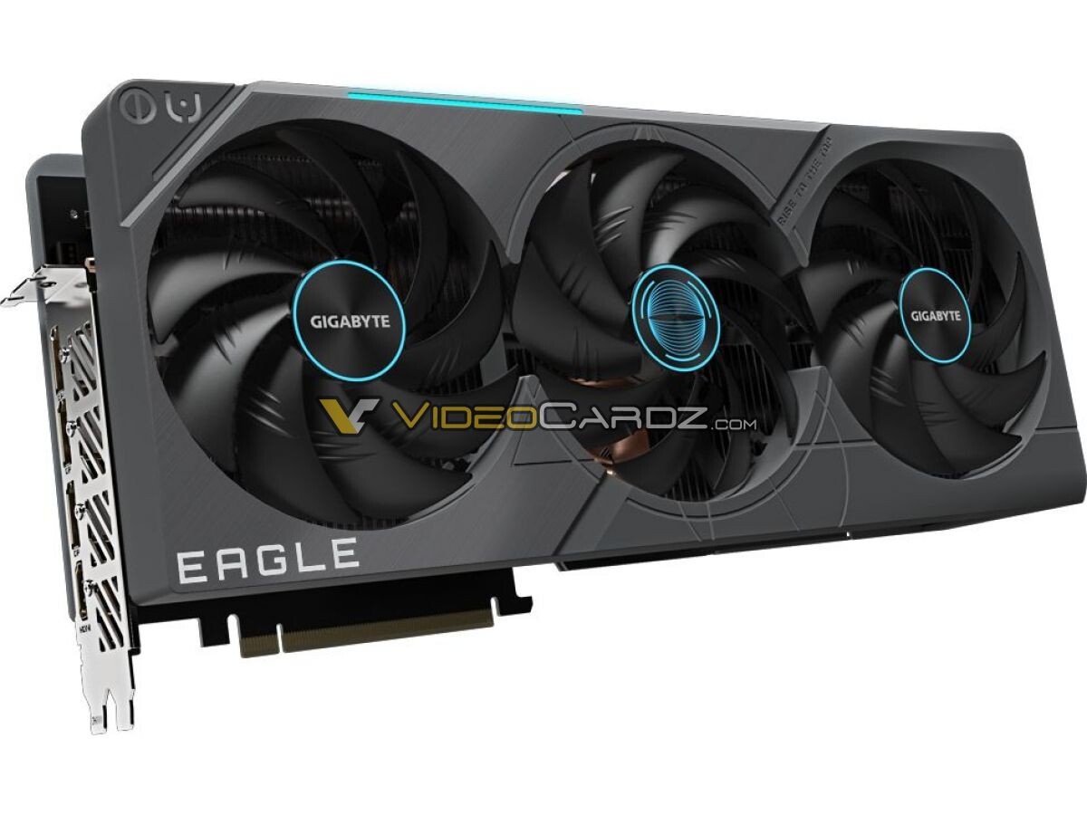
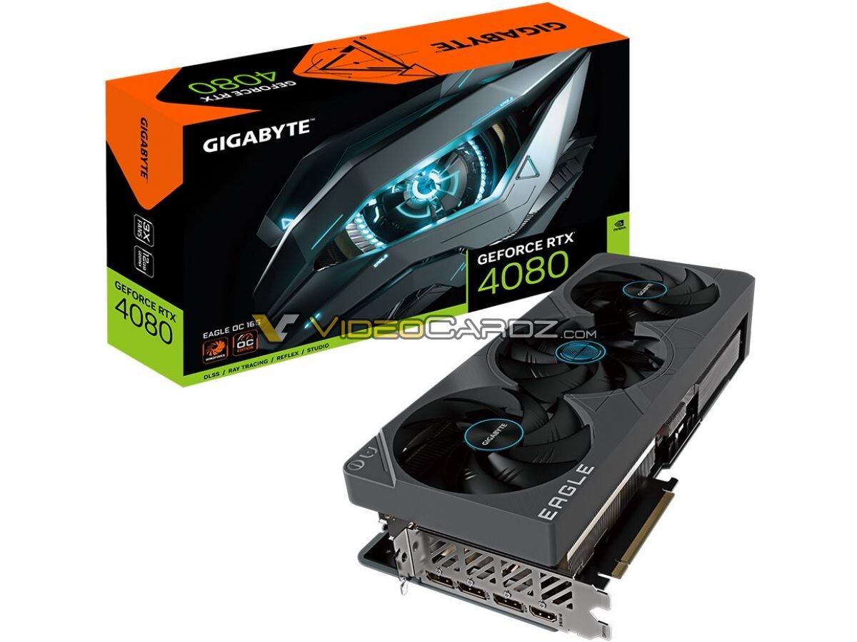
GIGABYTE GeForce RTX 4080 EAGLE Graphics Card Pictured
In case you missed it, NVIDIA "unlaunched" the GeForce RTX 4080 12 GB; and so the RTX 4080 16 GB is now called just "RTX 4080." Here are some of the first pictures of a custom-design RTX 4080, the GIGABYTE Eagle OC. The company's new value-ended factory-overclocked graphics card brand sheds much of the unnecessary design bulk of the RTX 30-series Eagle; and sticks with a functional, minimalist design. The card features a 4-slot cooling solution, with an enormous plastic cooler shrooud holding a trio of what look like 100 mm fans. ventilating a dual aluminium fin-stack heatsink. Display outputs include a trio of DisplayPort 1.4a, and an HDMI 2.0b. The card draws power from a single 16-pin 12VHPWR connector, and is possibly the first confirmation that NVIDIA is extending the new power connector down its product stack. The RTX 4080 has a typical board power of 320 W (at reference speeds).
Based on the 4 nm AD103 silicon, the RTX 4080 is endowed with 9,728 CUDA cores, 76 RT cores, 304 Tensor cores, 304 TMUs, and 112 ROPs. The card's 16 GB of GDDR6X memory runs across a 256-bit wide memory interface, which at its memory frequency of 23 Gbps, churns out 736 GB/s of memory bandwidth. GIGABYTE is designing the Eagle brand-extension to compete with the likes of the ASUS TUF Gaming, and MSI Ventus X. NVIDIA is launching the RTX 4080 on November 16.


Based on the 4 nm AD103 silicon, the RTX 4080 is endowed with 9,728 CUDA cores, 76 RT cores, 304 Tensor cores, 304 TMUs, and 112 ROPs. The card's 16 GB of GDDR6X memory runs across a 256-bit wide memory interface, which at its memory frequency of 23 Gbps, churns out 736 GB/s of memory bandwidth. GIGABYTE is designing the Eagle brand-extension to compete with the likes of the ASUS TUF Gaming, and MSI Ventus X. NVIDIA is launching the RTX 4080 on November 16.