News Posts matching #Cache

Return to Keyword Browsing

MSI Released AGESA COMBO PI V2 1.2.0.1 Beta BIOS for AMD 500 Series Motherboards

MSI, a world-leading motherboard manufacturer, announces the release of AGESA COMBO PI V2 1.2.0.1 beta BIOS for its AMD 500 series motherboards to add SMART ACCESS MEMORY support to AMD RYZEN 3000 desktop processors. Now both RYZEN 5000 and RYZEN 3000* desktop processors support SMART ACCESS MEMORY. AGESA COMBO PI V2 1.2.0.1 BIOS also improves L3 Cache bandwidth in AIDA64 for RYZEN 5000 desktop processors.

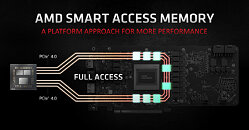
SMART ACCESS MEMORY is an innovative feature that allows the system to access the full capacity of the VRAM on the graphics card. Compare to the current solution which has a 256 MB access limitation, this feature will provide the users a better gaming experience.

AMD Patents Chiplet Architecture for Radeon GPUs

On December 31st, AMD's Radeon group has filed a patent for a chiplet architecture of the GPU, showing its vision about the future of Radeon GPUs. Currently, all of the GPUs available on the market utilize the monolithic approach, meaning that the graphics processing units are located on a single die. However, the current approach has its limitations. As the dies get bigger for high-performance GPU configurations, they are more expensive to manufacture and can not scale that well. Especially with modern semiconductor nodes, the costs of dies are rising. For example, it would be more economically viable to have two dies that are 100 mm² in size each than to have one at 200 mm². AMD realized that as well and has thus worked on a chiplet approach to the design.

AMD reports that the use of multiple GPU configuration is inefficient due to limited software support, so that is the reason why GPUs were kept monolithic for years. However, it seems like the company has found a way to go past the limitations and implement a sufficient solution. AMD believes that by using its new high bandwidth passive crosslinks, it can achieve ideal chiplet-to-chiplet communication, where each GPU in the chiplet array would be coupled to the first GPU in the array. All the communication would go through an active interposer which would contain many layers of wires that are high bandwidth passive crosslinks. The company envisions that the first GPU in the array would communicably be coupled to the CPU, meaning that it will have to use the CPU possibly as a communication bridge for the GPU arrays. Such a thing would have big latency hit so it is questionable what it means really.

AMD Big Navi GPU Features Infinity Cache?

As we are nearing the launch of AMD's highly hyped, next-generation RDNA 2 GPU codenamed "Big Navi", we are seeing more details emerge and crawl their way to us. We already got some rumors suggesting that this card is supposedly going to be called AMD Radeon RX 6900 and it is going to be AMD's top offering. Using a 256-bit bus with 16 GB of GDDR6 memory, the GPU will not use any type of HBM memory, which has historically been rather pricey. Instead, it looks like AMD will compensate for a smaller bus with a new technology it has developed. Thanks to the new findings on Justia Trademarks website by @momomo_us, we have information about the alleged "infinity cache" technology the new GPU uses.

It is reported by VideoCardz that the internal name for this technology is not Infinity Cache, however, it seems that AMD could have changed it recently. What does exactly you might wonder? Well, it is a bit of a mystery for now. What it could be, is a new cache technology which would allow for L1 GPU cache sharing across the cores, or some connection between the caches found across the whole GPU unit. This information should be taken with a grain of salt, as we are yet to see what this technology does and how it works, when AMD announces their new GPU on October 28th.

CacheOut is the Latest Speculative Execution Attack for Intel Processors

Another day, another speculative execution vulnerability found inside Intel processors. This time we are getting a new vulnerability called "CacheOut", named after the exploitation's ability to leak data stored inside CPU's cache memory. Dubbed CVE-2020-0549: "L1D Eviction Sampling (L1Des) Leakage" in the CVE identifier system, it is rated with a CVSS score of 6.5. Despite Intel patching a lot of similar exploits present on their CPUs, the CacheOut attack still managed to happen.

The CacheOut steals the data from the CPU's L1 cache, and it is doing it selectively. Instead of waiting for the data to become available, the exploit can choose which data it wants to leak. The "benefit" of this exploit is that it can violate almost every hardware-based security domain meaning that the kernel, co-resident VMs, and SGX (Software Guard Extensions) enclaves are in trouble. To mitigate this issue, Intel provided a microcode update to address the shortcomings of the architecture and they recommended possible mitigations to all OS providers, so you will be protected once your OS maker releases a new update. For a full list of processors affected, you can see this list. Additionally, it is worth pointing out that AMD CPUs are not affected by this exploit.

Intel Adds More L3 Cache to Its Tiger Lake CPUs

InstLatX64 has posted a CPU dump of Intel's next-generation 10 nm CPUs codenamed Tiger Lake. With the CPUID of 806C0, this Tiger Lake chip runs at 1000 MHz base and 3400 MHz boost clocks which is lower than the current Ice Lake models, but that is to be expected given that this might be just an engineering sample, meaning that production/consumer revision will have better frequency.

Perhaps one of the most interesting findings this dump shows is the new L3 cache configuration. Up until now Intel usually put 2 MB of L3 cache per each core, however with Tiger Lake, it seems like the plan is to boost the amount of available cache. Now we are going to get 50% more L3 cache resulting in 3 MB per core or 12 MB in total for this four-core chip. Improved cache capacity can result in additional latency because of additional distance data needs to travel to get in and out of cache, but Intel's engineers surely solved this problem. Additionally, full AVX512 support is present except avx512_bf which supports bfloat16 floating-point variation found in Cooper Lake Xeons.

Wishful Thinking, Disingenious Marketing: Intel's Optane Being Marketed as DRAM Memory

Intel's Optane products, based on the joint venture with Micron, have been hailed as the next step in memory technology - delivering, according to Intel's own pre-launch slides, a mid-tier, al-dente point between DRAM's performance and NAND's density and pricing. Intel even demoed their most avant-garde product in recent times (arguably, of course) - the 3D XPoint DIMM SSD. Essentially, a new storage contraption that would occupy vacant DIMM channels, delivering yet another tier of storage up for grabs for speed and space-hungry applications - accelerating workloads that would otherwise become constrained by the SATA or even NVMe protocol towards NAND drives.

Of course, that product was a way off; and that product still hasn't come to light. The marriage of Optane's density and speed with a users' DRAM subsystem is just wishful thinking at best, and the dreams of pairing DRAM and 3D Xpoint in the same memory subsystem and extracting the best of both worlds remains, well... A figment of the imagination. But not according to some retailers' websites, though. Apparently, the usage of Intel's Optane products as DRAM memory has already surfaced for some vendors - Dell and HP included. How strange, then, that this didn't come out with adequate pomp and circumstance.

Intel Optane MEM M10 Cache Modules Surface on Retailers' Websites

The next step in Intel's Optane product launch could be right around the corner, as retailers have started listing the company's upcoming Optane MEM M10 cache drives up for pre-order. If you'll remember, these products were first leaked in some Intel product roadmap slides, where they appeared identified as "System Acce. Gen 1.0". Whether or not today's workloads and faster SSD-based storage require the introduction of a faster caching solution is up for debate; however, Intel seems to think there is room in the market for these caching solutions, even if the vast majority of users would be much better served by acquiring a higher capacity SSD as their primary drive (especially if they're coming from the HDD world).

These new Optane MEM M10 cache drives will come in capacities ranging from 16 GB to 64 GB. The M10 modules will take the M.2 2280 form-factor and deliver data through the PCIe 3.0 interface. Prices are being quoted at $47.58 for the 16 GB model, $82.03 for the 32 GB model, and $154.37 for the largest, 64 GB model. These should ensure lower latency and higher throughput than traditional SSDs do, due to their caching of users' more heavily requested data; however, due to the very nature of these caching solutions, and the memory footprint available for them, it's likely most users will hit severe performance bottlenecks, at the very least, on the 16 GB model.

AMD's RX Vega to Feature 4 GB and 8 GB Memory

It looks like AMD is confident enough on its HBC (High-Bandwidth Cache) and HBCC (High-Bandwidth Cache Controller) technology, and other assorted improvements to overall Vega memory management, to consider 4 GB as enough memory for high-performance gaming and applications. On a Beijing tech summit, AMD announced that its RX Vega cards (the highest performers in their next generation product stack, which features rebrands of their RX 400 line series of cards to th new RX 500) will come in at 4 GB and 8 GB HBM 2 (512 GB/s) memory amounts. The HBCC looks to ensure that we don't see a repeat of AMD's Fury X video card, which featured first generation HBM (High-Bandwidth memory), at the time limited to 4 GB stacks. But lacking extensive memory management improvements meant that the Fury X sometimes struggled on memory-heavy workloads.

If the company's Vega architecture deep dive is anything to go by, they may be right: remember that AMD put out a graph showing how the memory allocation is almost twice as big as the actual amount of memory used - and its here, with smarter, improved memory management and allocation, that AMD is looking to make do with only 4 GB of video memory (which is still more than enough for most games, mind you). This could be a turn of the screw moment for all that "more is always better" philosophy.

AMD's Ryzen Cache Analyzed - Improvements; Improveable; CCX Compromises

AMD's Ryzen 7 lower than expected performance in some applications seems to stem from a particular problem: memory. Before AMD's Ryzen chips were even out, reports pegged AMD as having confirmed that most of the tweaks and programming for the new architecture had been done in order to improve core performance to its max - at the expense of memory compatibility and performance. Apparently, and until AMD's entire Ryzen line-up is completed with the upcoming Ryzen 5 and Ryzen 3 processors, the company will be hard at work on improving Ryzen's cache handling and memory latency.

Hardware.fr has done a pretty good job in exploring Ryzen's cache and memory subsystem deficiencies through the use of AIDA 64, in what would otherwise be an exceptional processor design. Namely, the fact that there seems to be some problem with Ryzen's L3 cache and memory subsystem implementation. Paired with the same memory configuration and at the same 3 GHz clocks, for instance, Ryzen's memory tests show memory latency results that are up to 30 ns higher (at 90 ns) than the average latency found on Intel's i7 6900K or even AMD's FX 8350 (both at around 60 ns).
Return to Keyword Browsing
Apr 22nd, 2025 02:17 EDT change timezone

New Forum Posts

Popular Reviews

Controversial News Posts