News Posts matching #G92b

Return to Keyword Browsing

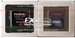
GK104 Silicon Roughly As Big As G92b

When the first PCB shot of the GK104 reference board surfaced, it sent the punters estimating the die area of the GK104 GPU, which the pinned at somewhere around 320 mm². A newer close-up picture of the GK104, helped calculate the figure more accurately, down to around 300 mm² (±5 mm²). This calculation also takes into account that the GK104 chip-package is as big as that of the G92, and the die just as big. It was compared alongside a 55 nm G92b chip. GK104 is NVIDIA's newest performance GPU built on the Kepler architecture, on which SKUs such as the GeForce GTX 680, are based.

EVGA and NVIDIA Design Unique Multi-GPU Graphics Accelerator

EVGA and NVIDIA are readying a unique multi-GPU graphics accelerator this Halloween, slated for October 30. To celebrate its launch, the two have organized a launch party for 300 lucky participants who will go to the NVIDIA Plaza in Santa Clara, CA and witness the launch of the new GeForce product. The accelerator packs two GPUs: a G200b, and a G92b. That's right, a GeForce GTX 200 series GPU, with a GeForce GTS 250 GPU. This is perhaps the first graphics accelerator to pack two entirely different GPUs. How it works, however, is interesting: the G200b GPU handles graphics, while the G92b is dedicated to PhysX processing. The accelerator could have 896 MB of graphics memory, with 512 MB of dedicated memory for the PhysX GPU. You can sign up for the event here.

GeForce GTS 240 Spotted in OEM Channels

NVIDIA's move to rebrand the GeForce 9800 GTX+ to GeForce GTS 250 was meant to be followed with a similar rebranding for the GeForce 9800 GT, to GeForce GTS 240. The company even prepared a reference PCB design for the accelerator. Alas, the move wasn't popular NVIDIA's partners, who forced it shelve the plans.

Apparently NVIDIA wants to continue development of the GeForce GTS 240, at least for its OEM customers, if not AIC partners that cater to the retail consumer segment. The GeForce GTS 240 reference design accelerator is in accordance with the schematics that surfaced back in February, and maintains a single-slot design overall. Under the hood is the 55 nm G92b graphics processor with 112 shader processors, a 256-bit GDDR3 memory interface, 1 GB of memory, and reference clock speeds that match that of GeForce 9800 GT OC: 675/1620/1100 (core/shader/memory). The card supports 2-way SLI, and should be priced in the sub $130 space.

GeForce GTX 200M, GTS 100M Series Unveiled

Reigning supreme again in the desktop segment, NVIDIA is looking forward to taking the wraps off its GeForce GTX 200M mGPU series. The new GPU series looks to up the performance offer by 50%, as claimed by the company. In the league are GeForce GTX 280M, GTX 260M and GTS 160M. Before you infer from the product names that at least two of them are based on the G200 graphics processor, let us break it to you, they're not. The entire series is based on the 55 nm G92b series. The 55 nm manufacturing technology seems to have facilitated some jumps in reference clock speeds.

Gigabyte GeForce GTS 250 w/ Zalman Cooling Spotted

As NVIDIA gears up to give GeForce GTS 250 a gala CeBIT launch, its partners seem to be ready with their products, and press-shots. Gigabyte will be one of the first to be out with a GeForce GTS 250 based graphics accelerator that uses the company's own design, GV-N250ZL-1GI. For those new, the GeForce GTS 250 is simply a re-launch of the NVIDIA's 9800 GTX+ accelerator. It is based on the same G92b core and uses identical specifications.

Gigabyte's first accelerator sports the Ultra Durable PCB construction. The PCB consists of 2 oz (56.6 g) copper layers that help spread heat and minimize ground electrical noise. It also consists of the all solid-capacitor, ferrite choke, low effective RDS on MOSFETs design. The most interesting feature of this card is its cooler: a Zalman VF1050. Heat is drawn from the GPU-contact block using four heatpipes that convey it to a dense array of copper fins, nucleated by a PWM-controlled fan. The clock speeds on this card remain close to the reference speeds: 740/1850/2000 MHz (core/shader/memory). It might hit the stores after NVIDIA makes the GPU official.

GeForce GTS 240 Reference PCB Schematics Surface

In the weeks to come, NVIDIA will release yet another graphics card based on the G92 graphics processor: the GeForce GTS 240, which bears resemblance with the 8800 GT and 9800 GT. The G92 GPU has near-identical specifications to the said graphics cards, except for that the 55 nm G92b GPU will be used, and with higher reference clock speeds of 675/1674/975 MHz (core/shader/memory). To seat the new GPU, NVIDIA has designed a new reference PCB, the P361 internally called D10P2. The schematic drawings of this has been sourced by VR-Zone.

The P361 PCB covers the basics of accommodating the G92b and eight GDDR3 memory chips connected to the GPU across a 256-bit wide bus. The distinct features of the PCB lie with its VRM area, with a 3+1 phase design. The PCB draws power from a 6-pin PCI-Express power connector. Over to the connectors department, the usual two arrangement of two DVI and one composite is present. There is a single SLI bridge connector for 2-way SLI. With the 55 nm GPU being arguably as cool or cooler than the 65 nm G92 with lower reference clock speeds, one can expect a single slot cooler design to be employed.

XFX GeForce GTS 250 Pictured, Looks Familiar

Come March 3, and NVIDIA will have officially renamed the GeForce 9800 GTX+ to GeForce GTS 250. NVIDIA partners will have announced new SKUs based on the GPU throughout March. XFX on its part, seems to have made its GTS 250 accelerator ready, and it looks familiar. Chinese website IT168 caught an early glimpse of the accelerator.

The XFX GeForce GTS 250 series card will use a custom cooling design that looks almost identical to the company's Radeon HD 4850 accelerator. It features a 55 nm G92b graphics processor. Its clock-speeds are expected to be 738/1836/1100 MHz (core/shader/memory) for the base model, though one might expect XFX to come up with factory-overclocked variants. It holds 512 MB of GDDR3 memory across a 256-bit memory bus. XFX may choose the upcoming CeBIT event to launch this accelerator, after of-course, NVIDIA handles the SKU launch on its end of things.

G92-Based GeForce 9 Series Products to be Renamed GeForce GTS 200 Series

The NVIDIA G92 graphics processor has had the reputation of spanning across two generations of GeForce graphics accelerators, which could well become three with talk about NVIDIA executing another re-branding to products based on the GPU. The re-branding will use the B1 revision of the G92 GPU (aka G92b), which is known to have been manufactured on the 55nm fabrication process, along with the 65nm A1 revision.

The new series created will include two SKUs based on the G92, the GeForce GTS 240 and GeForce GTS 250. These are the 112 SP and 128 SP variants of the G92 core, presently branded under 8800/9800 GT and 8800 GTS 512, 9800 GTX/GTX+ respectively. NVIDIA looks to capitalise on the sales improvement the GTX 200 series has seen for the past two or so months now, by giving it a present-generation branding. The re-branding, or rather, releasing products with the new naming scheme is said to be operationalised by February 2009.

NVIDIA Updates Chip Package Materials, 55nm GPUs subject to Changes too

A product change notification (PCN) document by NVIDIA The Inquirer claims to have access to, indicates changes to the bump materials of several NVIDIA graphics processors (GPUs). Affected by this change are popular GPUs such as G92 and G92b (55nm). Changes include replacement of a High-Pb solder (95% Pb / 5% Sn) bump material with Eutectic Solder (63% Sn / 37% Pb). Bumps are those parts of the die that establish electrical contact with the leads/pins of the FC-BGA package. Failures of these bumps are irreparable leading to permanent damage. This follows several events that lead to NVIDIA owning up defects in certain mobile graphics and MCP parts.

Implications of this PCN are:
  • Current G92 and G92b are weaker and could be subject to failures similar to those products already diagnosed with failing packages and official announcements issued.
Return to Keyword Browsing
Jun 27th, 2024 17:52 EDT change timezone

New Forum Posts

Popular Reviews

Controversial News Posts