News Posts matching #GK104

Return to Keyword Browsing

More GeForce GTX 690 Details Surface

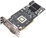
We know from older reports that NVIDIA is working on GeForce GTX 690, a dual-GPU graphics card based on the 28 nm GK104 silicon, we also know that its launch will be strategically timed to follow that of AMD Radeon HD 7990. Expreview scored a few juicy details about this card. To begin with, it is reported that GeForce GTX 690 will draw power from two 8-pin PCIe power connectors.

The GeForce GTX 690 will use a PCI-Express 3.0-compliant bridge chip. Its display outputs will include three DVI and one DisplayPort. PSU with at least 650W capacity will be made a system requirement. The entire feature-set of GeForce GTX 680 will be carried over. The exact specifications, core configuration, and memory amount, remain at large.
NVIDIA GK106 GPU Detailed

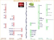
Following the launch of a couple of more GK104-based SKUs, namely GeForce GTX 670 Ti, and GeForce GTX 670, some time in May; NVIDIA will launch its third (after GK104 and GK107) Kepler architecture-based silicon, codenamed GK106. GK106 will make up sub-$200 SKUs, and succeeds the GF116, on which SKUs such as the GeForce GTX 550 Ti, are based. The GK106 will make up at least one known desktop SKU, called GeForce GTX 660.

Its specifications are listed below.

New GK104 SKU Details Surface

We know from a late-March article that NVIDIA is working on two new SKUs based on its GK104 silicon, for launch in May. With the Kepler architecture, particularly with the design of the new-generation Streaming Multiprocessors (SMX), NVIDIA substantially increased CUDA core density. Each SMX holds 192 CUDA cores, and as with the previous-generation Fermi architecture, the SMX count is the only thing NVIDIA can tinker with, to control CUDA core count in new GPUs. GeForce GTX 680's little brother, hence will have 7 out of 8 SMX units enabled, and end up with a CUDA core count of 1344. This leaves easier to configure parameters such as clock speeds, for NVIDIA to design the perfect SKU to capture a price-point. NVIDIA is targeting the sub-$399 market, while somehow maintaining competitiveness with Radeon HD 7950.

Specifications of the new SKU follow.

Colorful Makes GeForce GTX 680 iGame Kudan Official

Colorful announced its most powerful GTX 680 named "iGame GTX680-2G Kudan". The first "iGame Kudan" graphics card was released last year, and it was a GTX560Ti. Now Colorful uses the design concept on the latest GK104 chip.

Like the first generation, iGame GTX680 Kudan equipped a huge cooler which requires three slots and assembles three fans, one is 90mm, and others are 80mm and with "Shark Bionic" design in order to reduce the noise. Below the triple fans, there are heat-sinks which are crossed by ten 6mm heat-pipes. A 3mm steel plate is covered on the back of the PCB in order to enhance the PCB and improve the heat radiation.
ZOTAC GeForce GTX 680 Extreme Edition Pictured

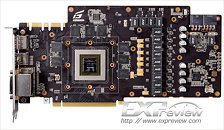
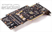
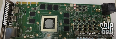
ZOTAC is flexing its engineering muscle. First, it was talk of a 2 GHz GeForce GTX 680 by one of its senior executives, and now this, ZOTAC GeForce GTX 680 Extreme Edition. Pictured below, the card's design is reminiscent of the crazy engineering endeavors ZOTAC China undertakes, to come up with some extremely powerful designs, which seldom get out of the APAC region (to EMEAI and NA regions).

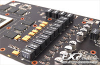
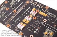
ZOTAC took a top-tier binned GK104 GPU, 2 GB of high-grade Hynix GDDR5 memory chips, and paired them with a 12-phase VRM power supply. Apart from bleeding-edge International Rectifier GaNpowIR driver-MOSFETs, the VRM uses server-grade tantalum capacitors, and FPCAP multi-phase capacitors. To drive it all, ZOTAC used CHiL CHL8318 VRM controller.

First Single-Slot, Air-Cooled GeForce GTX 680 Taking Shape

Single-slot advocates [in Asia, and select markets], your prayers are answered. Galaxy is working on a single-slot, air-cooled GeForce GTX 680. With a name that translates to "GeForce GTX 680 Warriors' Edition", Galaxy's card takes advantage of the fact that since very compact GK104 PCBs can be made, if dual-slot coolers are used, and since the TDP of the chip is a manageable 195W, the equation can be turned around to make long single-slot graphics cards.

Pictured below is the graphics card, with its [apparently] long cooler that protrudes beyond the length of the PCB. The cooler follows the same design principle at work in coolers of GeForce 8800 GT and Radeon HD 4850, that of a compact lateral-flow fan guiding air through a dense network of copper channels, where heat is dissipated to the air. These copper channels draw heat from a copper plate (probably vapor-chamber, in Galaxy's case), which makes contact with all hot components on the PCB, including the GPU, memory chips, and VRM. Hot air is guided out, from the top of the card. There is no further information about this card.

Did NVIDIA Originally Intend to Call GTX 680 as GTX 670 Ti?

Although it doesn't matter anymore, there are several bits of evidence supporting the theory that NVIDIA originally intended for its GK104-based performance graphics card to be named "GeForce GTX 670 Ti", before deciding to go with "GeForce GTX 680" towards the end. With the advent of 2012, we've had our industry sources refer to the part as "GTX 670 Ti". The very first picture of the GeForce GTX 680 disclosed to the public, early this month, revealed a slightly old qualification sample, which had one thing different from the card we have with us today: the model name "GTX 670 Ti" was etched onto the cooler shroud, our industry sources disclosed pictures of early samples having 6+8 pin power connectors.

Next up, while NVIDIA did re-christian GTX 670 Ti to GTX 680, it was rather sloppy at it. The first picture below shows the contents of the Boardshots (stylized) folder in NVIDIA's "special place" for the media. It contains all the assets NVIDIA allows the press, retailers, and other partners to use. Assets are distributed in various formats, the TIFF is a standard image-format used by print-media, for its high dot-pitch. Apart from a heavy payload, the TIFF image file allows tags, that can be read by Windows Explorer, these tags help people at the archives. The tags for images in TIFF format, of the GTX 680 distributed to its partners in the media and industry contain the tag "GTX 670 Ti".

GIGABYTE Out With its GeForce GTX 680

GIGABYTE took its own sweet time launching its GeForce GTX 680, but no harm done. Carrying the product code GV-N680D5-2GD-B, GIGABYTE's graphics card sticks to NVIDIA reference board design, decorated with a slick-looking abstract art. The card also sticks to NVIDIA reference clock speeds of 1006 MHz (core), 1058 MHz (boost), and 1502 MHz / 6.00 GHz effective GDDR5 memory. It is armed with 2 GB of memory sitting across a 256-bit wide memory interface. Based on the 28 nm GK104 GPU, NVIDIA GeForce GTX 680 is powered by 1536 CUDA cores, and a revolutionary, energy-efficient architecture. GIGABYTE GeForce GTX 680 is priced at US $499.

Club 3D Comes Up with a GeForce GTX 680 Too

Dutch board maker Club 3D has today joined the Kepler launch party and announced its very own GeForce GTX 680. Based on NVIDIA's reference design, Club 3D's card is equipped with one GK104 28 nm GPU, and features 1536 CUDA Cores, a base clock of 1006 MHz, a 256-bit memory interface, and 2 GB of GDDR5 VRAM set to 6000 MHz.

The GTX 680 packs a dual-slot cooler, has 3-way SLI support, and includes four display outputs (dual DVI, HDMI and DisplayPort), PCI-Express 3.0, and goodies like Adaptive V-Sync, single-card 3D Vision Surround, TXAA, and the NVENC video encoder. The Club 3D GeForce GTX 680 can be found listed @ 487 Euro.

GeForce GTX 680 SLI Performance Surfaces

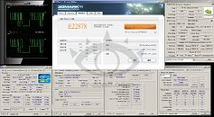
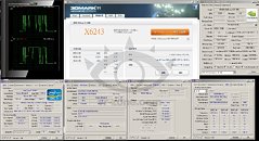
NVIDIA's big GeForce GTX 680 launch is just around the corner, but performance figures are already trickling in. Last week, we were treated to a wide range of benchmarks covering a single GeForce GTX 680. Today, VR-Zone posted a performance-preview of the GeForce GTX 680 in 2-way SLI configuration. A set of two GTX 680 cards were put through 3DMark 11 in Entry, Performance, and eXtreme presets. It should be noted here, that the GTX 680 cards were clocked at 1150 MHz core, and 1803 MHz (7.20 GHz effective) memory.

In the Entry preset, GTX 680 2-way SLI scored E22878; it scored P16860 in Performance preset; and X6243 in eXtreme. 2-way SLI of GTX 680 should be fit for 2560x1440/1600 resolution gaming. The rest of the test-bench consisted of Intel Core i7-3930K six-core processor clocked at 5.00 GHz, with 16 GB of quad-channel DDR3-2133 MHz memory, and ASUS ROG Rampage IV Extreme motherboard.

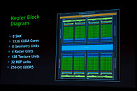
GK104 Block Diagram Explained

Specifications sheets of NVIDIA's GK104 GPU left people dumbfounded at the CUDA core count, where it read 1536, a 3-fold increase over that of the GeForce GTX 580 (3x 512). The block-diagram of the GK104, photographed at the NVIDIA press-meet by an HKEPC photographer, reveals how it all adds up. The GK104 is built on 28 nm fab process, with a die area of around 295 mm², according to older reports. Its component hierarchy essentially an evolution of that of the Fermi architecture.

The hierarchy starts with the GigaThread Engine, which marshals all the unprocessed and processed information between the rest of the GPU and the PCI-Express 3.0 system interface, below this, are four graphics processing clusters (GPCs), which holds one common resource, the raster engine, and two streaming multiprocessors (SMs), only this time, innovation has gone into redesigning the SM, it is called SMX. Each SMX has one next-generation PolyMorph 2.0 engine, instruction cache, 192 CUDA cores, and other first-level caches. So four GPCs of two SMXs each, and 16 SMXs of 192 CUDA cores each, amount to the 1536 CUDA core count. There are four raster units (amounting to 32 ROPs), 8 geometry units (each with a tessellation unit), and some third-level cache. There's a 256-bit wide GDDR5 memory interface.

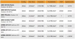
GK104 Transistor Count and Exact Die-Size Revealed

A part of the reason why NVIDIA's performance-segment GK104 is gunning for the performance crown from AMD's Tahiti GPU could be hidden behind two of its key specifications: transistor count, and die-size. 3DCenter.org compiled these two specifications for the GK104 from reliable sources, which pin the transistor count at 3.54 billion, and die-area at 294 mm². This yields a transistor density of 12 million per mm², which is slightly higher than that of AMD Tahiti, slightly lower than that of AMD Pitcairn, and certainly higher than previous-generation chips from both AMD and NVIDIA. If GeForce GTX 680 does in fact end up competitive with AMD's Radeon HD 7900 series, it could serve as a tell-tale sign of NVIDIA's Kepler architecture being a more efficient one.

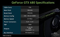
GeForce GTX 680 Specifications Sheet Leaked

Chinese media site PCOnline.com.cn released what it claims to be an except from the press-deck of NVIDIA's GeForce GTX 680 launch, reportedly scheduled for March 22. The specs sheet is in tune with a lot of information that we already came across on the internet, when preparing our older reports. To begin with the GeForce GTX 680 features clock speeds of 1006 MHz (base), and 1058 MHz (boost). The memory is clocked at a stellar 6.00 GHz (1500 MHz actual), with a memory bus width of 256-bit, it should churn out memory bandwidth of 192 GB/s. 2 GB is the standard memory amount.

For the umpteenth time, this GPU does feature 1,536 CUDA cores. The card draws power from two 6-pin PCIe power connectors. The GPU's TDP is rated at 195W. Display outputs include two DVI, and one each of HDMI and DisplayPort. Like with the new-generation GPUs from AMD, it supports PCI-Express 3.0 x16 bus interface, which could particularly benefit Ivy Bridge and Sandy Bridge-E systems, in cases where the link width is reduced to PCI-Express 3.0 x8 when there are multiple graphics cards installed.

Dual-GK104 Graphics Card Arrives in May

A little later this month, NVIDIA will launch the GeForce GTX 680, a single-GPU graphics card based on its GK104 performance GPU. It is reported that NVIDIA will design a dual-GPU graphics accelerator based on the same chip, which will then be positioned as an enthusiast product. Called the GeForce GTX 690, this dual-GPU solution will arrive in May.

NVIDIA's approach to the high-end segment, so far, is identical to that of AMD. It hasn't unveiled its enthusiast GK100 GPU, yet, and is instead using performance-segment GK104 for both its single-GPU high-performance graphics card, and as a dual-GPU part in an enthusiast-grade product. This buys NVIDIA plenty of time to release the GK100, unless AMD can offer a new GPU that trumps GK104 in performance, significantly.

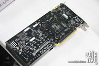
New NVIDIA GeForce GTX 680 Pictures Hit The Web

Courtesy of ChipHell we now have a couple of fresh pictures of NVIDIA's first Kepler-powered graphics card, the GeForce (or should we write' GeFORCE') GTX 680. Shot both from above and the back, the incoming card has a black PCB, a dual-slot/single-fan cooler, two (stacked) 6-pin PCIe power plugs, a couple of SLI connectors, and four display outputs - dual DVI, HDMI and DisplayPort.

The GTX 680 is equipped with one GK104 28 nm GPU, and reportedly boasts 1536 CUDA Cores, a 256-bit memory interface, 2 GB of GDDR5 VRAM (4 GB models should also be in the works), PCI-Express 3.0, and a TDP of around 190 W. The GeForce GTX 680 is expected to be launched next week, on March 22nd. Its rumored price tag is $549.

GK104 Silicon Roughly As Big As G92b

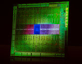
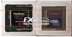
When the first PCB shot of the GK104 reference board surfaced, it sent the punters estimating the die area of the GK104 GPU, which the pinned at somewhere around 320 mm². A newer close-up picture of the GK104, helped calculate the figure more accurately, down to around 300 mm² (±5 mm²). This calculation also takes into account that the GK104 chip-package is as big as that of the G92, and the die just as big. It was compared alongside a 55 nm G92b chip. GK104 is NVIDIA's newest performance GPU built on the Kepler architecture, on which SKUs such as the GeForce GTX 680, are based.

More Pictures of GK104 Reference Board Surface

Here is a brief compilation of all the new images of the upcoming NVIDIA GeForce Kepler high-performance product, which our forum members posted through the day. The pictures reinforce the 3QTR picture that surfaced this Thursday, and full-length picture of the PCB that surfaced earlier this month. The first picture below, reveals what is essentially the card that was pictured yesterday, with its cooler shroud taken out. You will find a conventional air-channel cooler design. A lateral-flow fan, which looks similar to the one used in GeForce GTX 580/570), directs air through a dense aluminum channel array, which draws heat from key components such as the GPU, memory, and VRM, using a vapor-chamber plate (again, similar to the one used on high-end GeForce GTX 500 series). Towards the rear portion, you'll spot the piggy-backed 6+6-pin PCIe power connector cluster. You will also find the black rugged metal base-plate flowing along the full length of the PCB, structurally reinforcing it, and performing some cooling functions.

Moving on, the second picture reveals the same VRM area we saw earlier, on the green-colored PCB engineering sample, with its five NVVDD phases. The third picture is the first, of the reverse side of the PCB. Revealing most of the solder points, and electrical circuitry. The driver ICs of each of the NVVDD phases can be seen here. These two pictures confirm that the retail version of the GK104 product will feature a black PCB (the brown tinge is natural, due to the dense network of traces and ground layers, made of copper). The fourth picture reveals what looks like NVIDIA's Media Kit. Reputed reviewers get a NVIDIA-branded "media kit", which contains the graphics card sample to review, and other relevant documentation in printed form, along with a driver CD, and other accessories. These cards are not branded by any AIC partner, and are 100% compliant to NVIDIA's reference design and clock speeds.

Many Thanks to our community members JaredPace and CrapDaddy.

GK104 Dynamic Clock Adjustment Detailed

With its GeForce Kepler family, at least the higher-end parts, NVIDIA will introduce what it calls Dynamic Clock Adjustment, which adjusts the clock speeds of the GPU below, and above the base-line clock speeds, depending on the load. The approach to this would be similar to how CPU vendors do it (Intel Turbo Boost and AMD Turbo Core). Turning down clock speeds under low loads is not new to discrete GPUs, however, going above the base-line dynamically, is.

There is quite some confusion regarding NVIDIA continuing to use "hot clocks" with GK104, the theory for and against the notion have been enforced by conflicting reports, however we now know that punters with both views were looking at it from a binary viewpoint. The new Dynamic Clock Adjustment is similar and complementary to "hot clocks", but differs in that Kepler GPUs come with a large number of power plans (dozens), and operate taking into account load, temperature, and power consumption.

GK104 Graphics Card Pictured?

Could this be the very first picture of NVIDIA's GeForce Kepler 104-based graphics card? This Mr. Blurrycam shot has been doing rounds in Chinese forums. While it may not seem convincing at first glance, several features of the card in the picture seem to match the layout of the GK104 reference PCB which was pictured, earlier. To begin with, on the top-right corner you can train your eyes to a deep cutout, for the unusual piggy-backed 6+6 pin PCIe power connectors. The rear panel bracket is a 100% match (in layout and design of exhaust vents), of the one with the true-color image of the GK104 PCB. The only feature that clouds the plausibility of this picture is "GeForce GTX 670 Ti" being etched onto the cooler's shroud. We're hearing more voices refer to the top GK104 part as "GeForce GTX 680" than "GTX 670 Ti". We're also hearing that NVIDIA will adopt a new GeForce logo, so that glaring "GEFORCE" badge on the top of the card looks plausible.

UPDATE: Added less blurry picture.

GeForce GTX 680 Features Speed Boost, Arrives This Month, etc., etc.

Here are some key bits of information concerning the upcoming GeForce GTX 680, a performance single-GPU graphics card based on the 28 nm GK104 GPU by NVIDIA. The information, at face value, is credible, because we're hearing that a large contingent of the media that finds interest in the GPU industry, is attending the Game Developers Conference, where it could interact with NVIDIA, on the sidelines. The source, however, is citing people it spoke to at CeBIT.

First, and most interesting: with some models of the GeForce 600, NVIDIA will introduce a load-based clock speed-boost feature (think: Intel Turbo Boost), which steps up clock speeds of the graphics card when subjected to heavy loads. If there's a particularly stressing 3D scene for the GPU to render, it overclocks itself, and sees the scene through. This ensures higher minimum and average frame-rates.

GK104 (GTX 680) Has 17% Higher Compute Power Than Tahiti (HD7970): Report

A report by 3DCenter.org, which takes into account the specifications of NVIDIA's GK104 GPU, based on clock-speed and specs. leak estimated its shader compute power to be 17% higher than that of AMD's Tahiti in its Radeon HD 7970 avatar (4.46 TFLOPs single-precision floating point). Based on the said specifications, the report also hypothesized things such as memory bandwidth, ROP performance, and texture performance; and compared it to those of the Radeon HD 7970 and Radeon HD 7950.

GeForce GTX 680 Final Clocks Exposed, Allegedly

Waiting on Kepler before making a new GPU purchase? Well, you have to wait a little longer. Thankfully, this wait can be eased with the latest leaks about NVIDIA's 28 nm chip and the GeForce GTX 680 it powers.

According to VR-Zone, the GTX 680 does indeed feature 1536 CUDA Cores and a 256-bit memory interface, but it also has hotclocks, meaning the GPU is set to 705 MHz but the shaders operate at 1411 MHz. The memory (2 GB most likely) is supposed to be clocked at 6000 MHz giving a total memory bandwidth of 192 GB/s.

NVIDIA's incoming card is 10 inches long and also has 3-way SLI support, and four display outputs - two DVI, one HDMI and one DisplayPort. The GeForce GTX 680 is expected to be revealed on March 12 and should become available on March 23rd.

GK104 Die-Size Estimated

Thanks to some good understanding of geometry, and great Photoshop skills, the punters have estimated the die-size of NVIDIA's GeForce Kepler 104 (GK104) GPU, using a picture of the NVIDIA reference board that was leaked last week. Compared to the known die-size of an AMD "Tahiti"-based graphics card, the die-size of GK104 was estimated to be around 320 mm², about 45 mm² smaller than Tahiti. The relative transistor density of the chip, compared to AMD's 28 nm chips, were also estimated.

GK104 PCB Pictured in Full

Here is the first true-color picture of the GeForce Kepler 104 (GK104) reference PCB shot in full (well, almost, excluding the uneventful PCIe bus connector). The picture provides a panoramic view of the card's VRM as shown in a drawing posted earlier this day, and reveals the strange double-decker power connector. The card is loaded with a 5-phase NVVDC configuration, as detailed in an older article. It also confirms that the GK104 has a 256-bit wide memory interface, with likely 2 GB standard memory amount. This is also the first picture of the GK104 ASIC, which has square package, and somewhat square die. While the PCB is green in color, it's most likely an engineering sample. The final product (branded GeForce GTX 680 / GTX 670 Ti), could have a black-colored one.

NVIDIA GK104 PCB Drawings, Unusual Power Connector Designs Surface

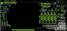
Here is the first x-ray drawing of NVIDIA's GeForce Kepler 104 (GK104) reference board, outlining the VRM area. The GPU and memory areas are blanked out for some very obvious reasons. Nevertheless, there's plenty of fascinating stuff going on in these pictures. To begin with, the picture confirms that the board will have 5 NVVDD phases, and up to three miscellaneous power domains. The PCB has provisions for two 6-pin and one 8-pin connector.

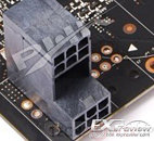
The funny part here is a strange new plug that has two 6-pin (or 8-pin+6-pin) stacked, while one of the two 6-pin connector leads are blanked. Some of our sources also report having seen a similar connector with 8-pin and 6-pin on samples of this card (refer to the last picture below). It's not just this, that makes the card incapable of single-slot operation, the DVI connectors over at the display IO also are stacked like on previous-generation AMD Radeon cards. Other connectors on the card are HDMI and DisplayPort. There are two SLI bridge connectors, giving it 3-way and 4-way SLI support.
Return to Keyword Browsing
Dec 26th, 2024 08:56 EST change timezone

New Forum Posts

Popular Reviews

Controversial News Posts