News Posts matching #GK104

Return to Keyword Browsing

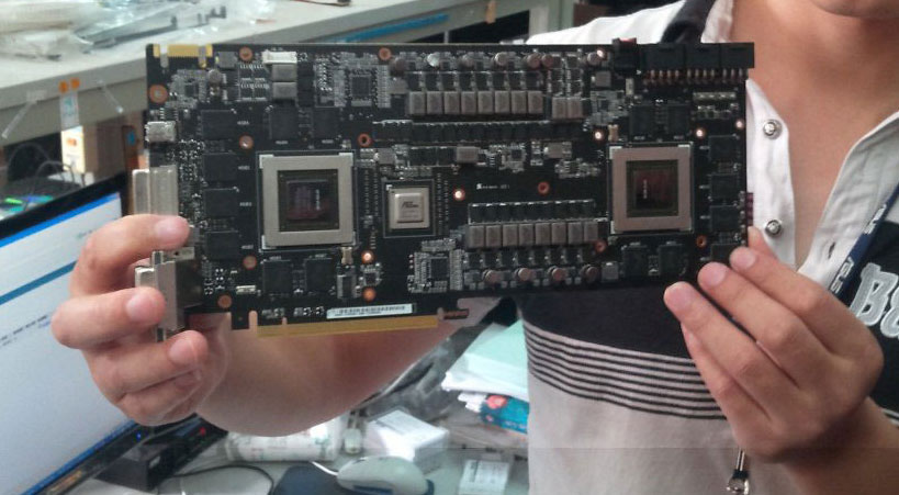
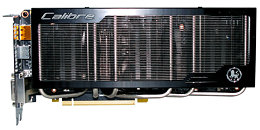
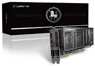
Sparkle Announces the Calibre X680/X670 Captain Graphics Cards

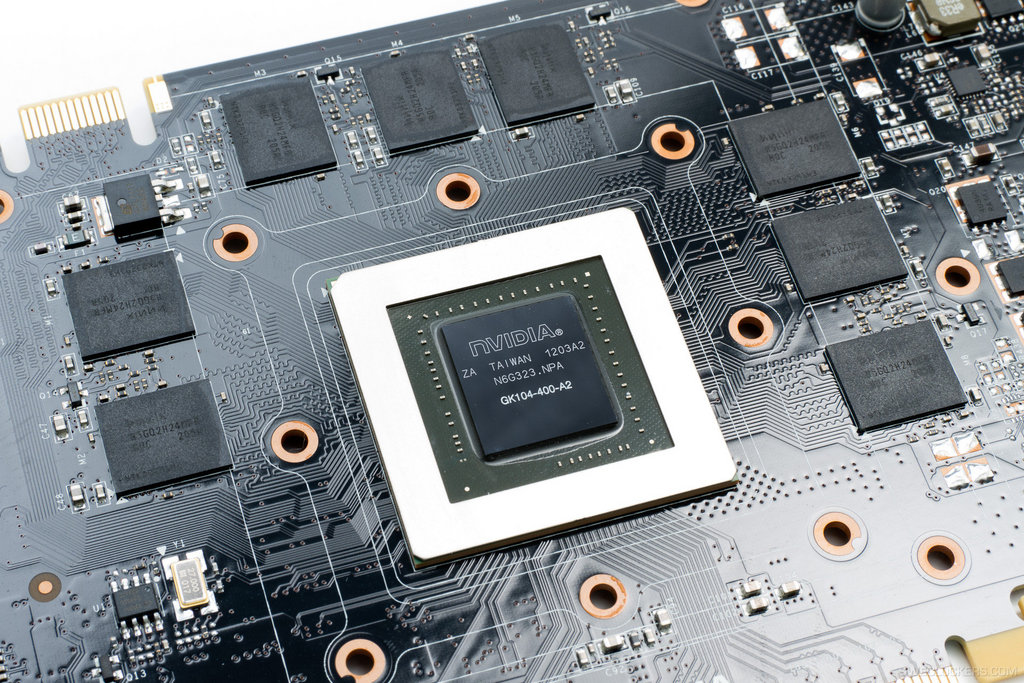
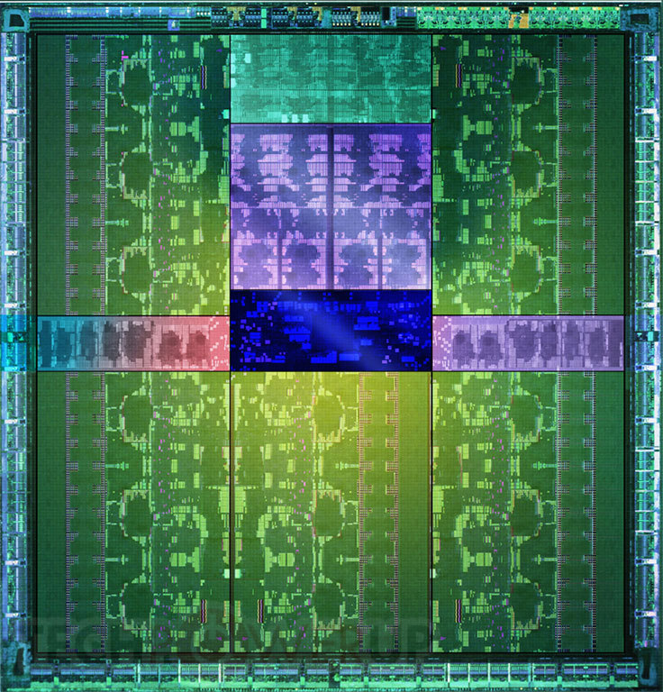
Calibre, one of industry leading brands of graphics solutions, launches the latest products, Calibre X680 Captain & Calibre X670 Captain, powered by NVIDIA's TOP 28 nm Kepler engine - GK104.

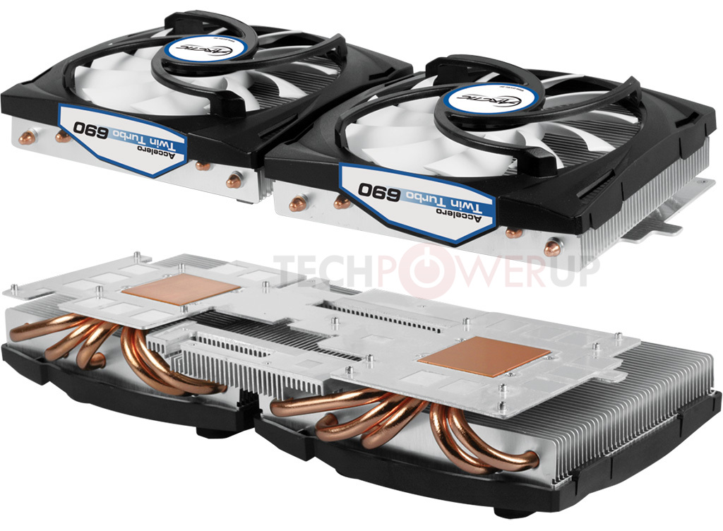
Calibre Series Returns with Maximum Performance

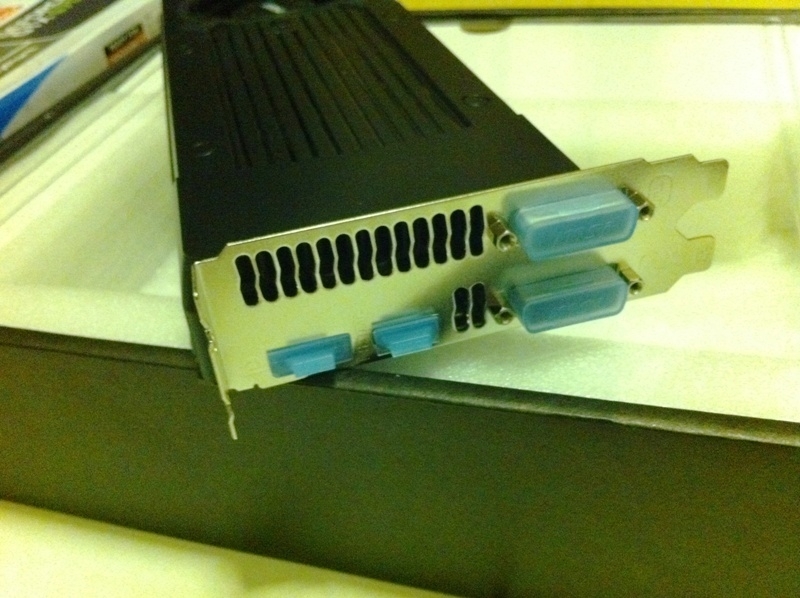
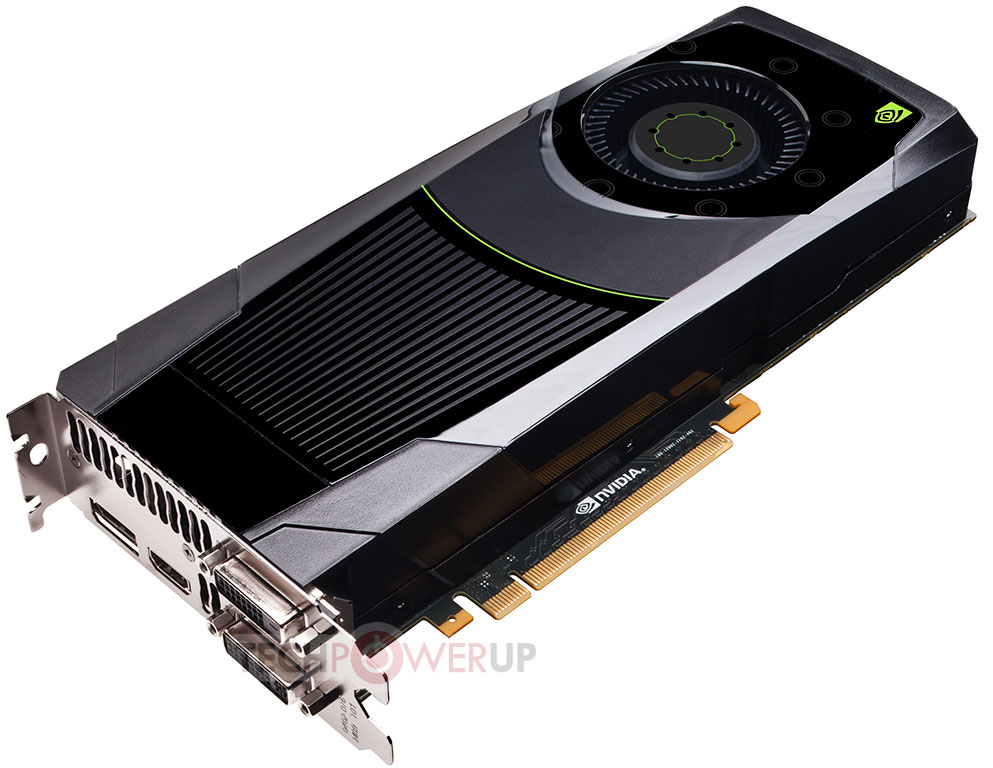
As the flagship product line of Calibre, Captain Series brings the tremendous different from reference design by tweaking the performance and cooling system, bringing the tremendous different from reference design. Moreover, Calibre X680/ X670 Captain Series preloaded overclocking value for enthusiasts.
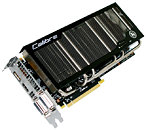
ASUS ROG MARS III Dual GTX 680 PCB Pictured

ASUS' Republic of Gamers MARS III dual-GeForce GTX 680 graphics card may have been extensively covered at this year's Computex event, but very few have had a peek at its innards (PCB). Expreview posted pictures of the card's PCB, sourced from the manufacturer.

The pictures reveal an unusually long and tall PCB, which draws power from three 8-pin PCIe power connectors, a 21-phase VRM that uses Super Alloy chokes and driver-MOSFETs, PLX PEX8747 PCI-Express 3.0 x48 bridge chip, and of course the two GK104 GPUs with a total of 32 individual GDDR5 memory chips (16 for each GPU, 16 on each side of the PCB) wired to them, totaling 8 GB of memory.

Edit: We received an update from ASUS, clarifying that this card will not be released. The design was only displayed during a factory tour, to show ASUS craftmanship.

Arctic Unveils Accelero Twin Turbo 690 VGA Cooler for GeForce GTX 690

Arctic unveiled its newest graphics card cooler, the Accelero Twin Turbo 690, for NVIDIA's top-of-the-line GeForce GTX 690 dual-GPU graphics card. The cooler offers 14% lower temperatures, and more importantly, 92% lower noise output at maximum load. The Accelero Twin Turbo 690 is a complex cooler, which uses a pair of primary heatsinks that make contact with the two GK104 GPUs, in combination with a secondary heatsink that draws heat from memory, bridge chip, VRM, and other hot ancillary components, which are ventilated by a pair of 120 mm 400-1500 RPM PWM-controlled fans.

The Arctic Accelero Twin Turbo measures about 288 (L) x 138 (W) x 50 (H) mm, and weighs about 800 g. As such, it doesn't make your GTX 690 much thicker than two expansion card slots would allow. It uses as many as ten 6 mm-thick copper heat pipes to transport heat from the bases to the various heatsinks. The cooler has a maximum thermal capacity of 400W. Arctic plans to make the Accelero Twin Turbo 690 available by 10th of September, priced at US $169.95.

GeForce GTX 660 OEM Specifications Surface, Blueprint to the Retail Version?

58NVIDIA posted the product page of its GeForce GTX 660 (non-Ti) graphics processor. The chip is currently marked as OEM-only, meaning only NVIDIA's OEM partners have access to it. Its specifications make us believe that the "real thing" (retail version) could be very similar to it.

To begin with, the GTX 660 OEM appears to be based on the same GK104 silicon as the GTX 660 Ti retail. It appears to have been carved out by disabling two SMX units, resulting in a CUDA core count of 1,152. The GPU core is clocked at 823 MHz, with 888 MHz GPU Boost. The memory is clocked at 1450 MHz (5.80 GHz GDDR5-effective), in combination with the 192-bit memory bus width, it churns out 134 GB/s memory bandwidth. Unlike the GTX 660 Ti with its standard memory amounts of 2 GB or 3 GB, the GTX 660 OEM has standard memory options of 1.5 GB and 3 GB. The rest of its feature-set is consistent with that of every other GeForce Kepler family GPU. The GeForce GTX 660 retail could be launched some time in September. It's not necessary that its specifications could match with the OEM version.

Galaxy GeForce GTX 660 Ti 2GB GC and 3GB GC Launched

Galaxy kicked off its GeForce GTX 660 Ti lineup with three models, the GTX 660 Ti 2 GB, the GTX 660 Ti 2 GB GC (factory-overclocked), and the GTX 660 Ti 3GB GC. The 2 GB variants use Galaxy's cost-effective twin-fan cooling solution, combined with a custom-design PCB that draws power from 6+8 pin power connectors. The GC variant offers clock speeds of 1006 MHz core, 1084 MHz GPU Boost, and 6.00 GHz memory. It achieves 2 GB of memory across a 192-bit wide memory interface using eight 2 Gbit memory chips, in which four chips share two 32-bit wide paths.

Galaxy's 3 GB GeForce GTX 660 Ti GC comes with the same clock speeds as the 2 GB GC, 1006 MHz core, 1084 MHz GPU Boost, and 6.00 GHz memory, but uses the higher-grade dual-fan cooler which has been featured on GeForce GTX 670 and GTX 680 graphics cards by the company. It uses the same exact PCB as the GTX 680. It achieves 3 GB of memory using twelve 2 Gbit memory chips, two chips per 32-bit wide path. Based on the 28 nm GK104 silicon, the GeForce GTX 660 Ti packs 1344 CUDA cores, 112 TMUs, 24 ROPs, and a 192-bit wide GDDR5 memory interface.

ASUS Announces GeForce GTX 660 Ti DirectCu II Graphics Cards

ASUS announced as many as five GeForce GTX 660 Ti graphics card models. The cards are based on the company's dual-slot DirectCu II cooling solution, and a PCB design that's similar to that of the GeForce GTX 670 DirectCu series. Among the five models are the GTX660 TI-DC2-2GD5, the base model that sticks to NVIDIA reference clock speeds of 915/980/6008 MHz (core/boost/memory); the GTX660 TI-DC2O-2GD5, with a mild level of factory-overclocking, at 967/1058/6008 MHz; GTX660 TI-DC2T-2GD5, or TOP variant, with 1059/1377/6008 MHz; and variants of the GTX660 TI-DC2O-2GD5 and GTX660 TI-DC2T-2GD5 that feature Steam coupons to Borderlands 2 game.

Based on the 28 nm GK104 silicon, the GeForce GTX 660 Ti packs 1344 CUDA cores, 112 TMUs, 24 ROPs, and a 192-bit wide memory interface, holding 2 GB of memory. ASUS' cards uses two 6-pin PCIe power connectors to draw power. Display outputs include a pair of dual-link DVI, and one each of HDMI and DisplayPort. The cards are 3-way SLI capable. The DirectCu II cooler uses a compound heatsink to which heat is fed by a number of copper heat pipes, which make direct contact with the GPU. ASUS plans 3 GB variants of the same models, in which six 2 Gbit memory chips make up 3072 MB of memory, with 144 GB/s memory bandwidth.

NVIDIA Announces the GeForce GTX 660 Ti

NVIDIA launched the GeForce GTX 660 Ti graphics processor. The new chip is designed to let NVIDIA capture a key sub-$350 price-point, and is designed to offer high performance per Dollar in its market segment. Its rival from the red camp is the Radeon HD 7950. Based on the same GK104 silicon as most other high-end GeForce GTX 600 series graphics cards, the GTX 660 Ti packs 1344 CUDA cores, 112 TMUs, 24 ROPs, and a 192-bit wide GDDR5 memory interface, holding 2 GB of memory. Most GeForce GTX 660 Ti graphics cards being launched today are of custom-design with prices ranging between $299 and $349.

Gigabyte GeForce GTX 670 WindForce 2X Graphics Card Pictured

Here are some of the first pictures of Gigabyte GeForce GTX 670 WindForce 2X graphics card, which was released towards the end of July, without much fuss. The pictures reveal what is a combination of a non-reference design compact PCB design by Gigabyte, making use of its Ultra Durable VGA component selection (2 oz copper PCB, Japanese solid-state capacitors, binned memory chips, ferrite core chokes, low RDS (on) MOSFETs), and its WindForce 2X cooler. The PCB uses a 4+2 phase VRM to power the GK104 GPU. It draws power from two 6-pin PCIe power connectors.

The card ships in two variants, one that sticks to NVIDIA-reference clock speeds, and an OC variant (941 MHz core, 1019 MHz GPU Boost, 6.00 GHz memory). The cooler uses a compound heatsink. Its design consists of a main central aluminum heatsink which draws heat from the GPU, while two satellite aluminum fin heatsinks draw heat from the GPU through two 8 mm-thick copper heat pipes. The heatsink is ventilated by a pair of 100 mm fans, which spin at low speeds and claim low noise levels. Gigabyte's WindForce 2X graphics card is expected to cost less than its flagship WindForce 3X. Find a review at the source.

GeForce GTX 660 Ti Specifications and Launch Date Released

According to the latest set of specifications scored by SweClockers, NVIDIA's upcoming performance-segment GPU, the GeForce GTX 660 Ti, is not much different from the GTX 670. The GTX 660 Ti is based on the 28 nm GK104 GPU, with 1,344 CUDA cores enabled - the same number as that on the GTX 670. What's more, the clock speeds don't differ between the two, either - 915 MHz core, 980 MHz GPU Boost, and 6.00 GHz GDDR5-effective memory.

The memory amount stays 2 GB, as well. It's just that the memory bus width is reduced from 256-bit to 192-bit, resulting in 25% lower memory bandwidth. The 2 GB of memory is spread across the 192-bit memory bus, probably with four chips using 32-bit wide paths each, with four other chips sharing two 32-bit wide paths. NVIDIA is known for pulling off such memory configurations, like it did with the GeForce GTX 550 Ti.

GeForce GTX 660 Arrives Mid-August: Report

NVIDIA's newest product designed to strike the price-performance "sweetspot," the GeForce GTX 660, is set for a mid-August market launch, according to a SweClockers report. The new chip could roll out some time between August 13 and 19. Given that other Kepler-based SKUs have been launched on Tuesdays or Thursdays, it's likely that the launch date could be either the 14th, or the 16th. The GTX 660 will be based on the 28 nm "GK104" GPU. It will feature 1,344 or 1,152 CUDA cores, and a 192-bit wide GDDR5 memory interface, holding 1.5 GB of memory, according to the report. The new GPU could capture a crucial sub-$300 price-point.

MSI Launches the GeForce GTX 680 Lightning Graphics Card

Leading mainboard and graphics card maker MSI has just announced the release of the N680GTX Lightning, the new king of the graphics card world equipped with the NVIDIA GeForce GTX 680 GPU. The N680GTX Lightning utilizes proprietary Unlocked Digital Power architecture to unleash the full performance of the graphics card without any extra modifications. The innovative patented GPU Reactor power supply back plate also reduces power supply noise and improves overclocking stability. the N680GTX Lightning is kept cool by the Twin Frozr IV cooling solution with Dust Removal technology, dual temperature-controlled fan setup and SuperPipe.

ZOTAC GeForce GTX 670 TwinCooler Graphics Card Detailed

One aspect of NVIDIA's GeForce GTX 670 that blew us away, was its unusually short PCB for a high-performance GPU. NVIDIA's reference board still ended up being of average length, because NVIDIA's lateral-flow cooling assembly protruded beyond the PCB's length. AIC partners such as ZOTAC realised that custom-design graphics cards with short PCBs can be made to stay short, by opting for top-flow cooling solutions, something it materialised with the new GTX 670 TwinCooler (model: ZTGTX670-2GD5TCR001/ZT-60305-10P).

Pictured below, the GTX 670 TwinCooler from ZOTAC is short (about 60 mm shorter than NVIDIA reference design card). It uses a dense aluminum fin heatsink to cool the GK104 GPU, memory, and VRM. The heatsink is ventilated by two 80 mm fans. The card needs just a tiny bit more than two expansion slots in your system, it appears like it won't block the third expansion card slot. Despite its diminutive form, the card is factory-overclocked, with 954 MHz GPU clock, 1033 MHz GPU Boost, and 6208 MHz memory (against reference speeds of 915/980/6008 MHz). It draws power from two 6-pin PCIe power connectors, outputs include two dual-link DVI, and one each of HDMI and DisplayPort. It will be launched on the 20th of June.

ASUS ROG MARS III Dual GTX 680 Graphics Card Detailed

The ROG MATRIX 7970 wasn't the only new Republic of Gamers graphics card on display at Computex, it was sitting next to the MARS III. This monstrosity is a dual-GeForce GTX 680 graphics card, it packs two 28 nm GK104 GPUs with clock speeds that match or exceed those of the GeForce GTX 680. ASUS stopped short of revealing the clock speeds. The card draws power from three 8-pin PCI-Express power connectors, next to it is an instant fan-override button that revs up the card's fans to 100%. The card gives out three dual-link DVI display outputs, and is capable of driving 3D Vision Surround using three >1920x1200 pixels displays. Unlike the MATRIX 7970 and countless recent examples of ASUS' ugly fixation with triple-slot cooling solutions, it's a pleasant surprise seeing that the triple-fan cooling solution of the MARS III needs just two expansion card slots. The MARS III will be manufactured in limited quantities, and will probably cost more than a GeForce GTX 690.

ELSA Catches Up With Its Gladiac GeForce GTX 670 Graphics Card

Japanese company ELSA, which specializes in Quadro and GeForce graphics cards, finally unveiled its Gladiac GeForce GTX 670 graphics card (model: GD670-2GERX). Pictured below, the ELSA's card sticks to NVIDIA reference design, except for the color of the PCB. It even sticks to reference clock speeds of 915 MHz core, 980 MHz GPU Boost, and 6008 MHz memory (GDDR5 effective). Based on the 28 nm GK104 silicon, the GTX 670 packs 1344 CUDA cores, a 256-bit wide GDDR5 memory interface, holding 2 GB of memory, on this card. It is priced at 52,800 JPY.

NVIDIA Readies GK104-based GeForce GTX 680M for Computex

NVIDIA is readying a high-performance mobile GPU for a Computex 2012 unveiling. Called the GeForce GTX 680M, the chip is based on its trusty 28 nm GK104 silicon, but with about half its streaming multiprocessors disabled, resulting in a CUDA core count of around 768. Reference MXM boards of the chip could ship with memory options as high as 4 GB, across a 256-bit wide memory interface. With the right craftsmanship on the part of NVIDIA, the GTX 680M could end up with a power draw of 100W. A Chinese source had the opportunity to picture the reference board qualification sample, and put it through 3DMark 11, in which it was found to be roughly 37% faster than the GF114-based GeForce GTX 670M, scoring 4905 points in Performance preset. The test bed was driven by Intel Core i7-3720QM quad-core mobile processor.

NVIDIA Pioneers New Standard for HPC With Tesla GPUs Built on Kepler Architecture

NVIDIA today unveiled a new family of Tesla GPUs based on the revolutionary NVIDIA Kepler GPU computing architecture, which makes GPU-accelerated computing easier and more accessible for a broader range of high performance computing (HPC) scientific and technical applications.

The new NVIDIA Tesla K10 and K20 GPUs are computing accelerators built to handle the most complex HPC problems in the world. Designed with an intense focus on high performance and extreme power efficiency, Kepler is three times as efficient as its predecessor, the NVIDIA Fermi architecture, which itself established a new standard for parallel computing when introduced two years ago.

MSI Announces the GeForce GTX 670 with GPU Overvoltage

Today leading international mainboard and graphics card maker MSI officially announces the new GeForce GTX 670 graphics card featuring the latest 28nm GeForce GTX 670 GPU and 2GB GDDR5 memory; supports PCI Express 3.0 standard to provide better performance and power efficiency than previous generation. The GeForce GTX 670 graphics card features NVIDIA's GPU Boost technology which allows the core clock to be automatically adjusted on the fly for optimal in-game performance.

When used with the MSI Afterburner overclocking utility, the power limit and clock offset can be adjusted as well for better overclocking capability; GPU overvoltage function to boost overclocking potential up to 22%! A single card is able to also support NVIDIA 3DVision Surround technology for up to four monitors to give gamers the best in-game experience.

NVIDIA's GeForce GTX 670 Short PCB Pictured Up Close

Thanks to the impressive power-draw and temperature figures its GeForce GTX 680 could come up with, NVIDIA's newest SKU based on the 28 nm GK104 silicon, the GeForce GTX 670, will feature a compact PCB. The reverse side of this PCB was first pictured on a Colorful-branded graphics card. A picture of its obverse side was posted earlier today. In comparison to the GTX 680, the GTX 670 PCB is quite short. The eight GDDR5 memory chips are distributed between both the sides, these chips are wired to the GPU over a 256-bit wide memory interface. The VRM area is pushed towards the front-end of the PCB. It consists of a 4+2 phase design. The card draws power from two 6-pin PCIe power connectors. Display outputs include two dual-link DVI, and one each of HDMI and DisplayPort. There are two SLI bridge connectors, giving it 4-way SLI capability.

Galaxy Readies Single-Slot GeForce GTX 670

A little later this week, NVIDIA will launch its third SKU based on the GK104 silicon, targeting key performance-segment price points, the GeForce GTX 670. It is possible that NVIDIA will allow AIC partners to come up with custom-designs from day one. One such designs is Galaxy's, which needs no more than one expansion slot in your system. Galaxy's single-slot GeForce GTX 670 appears to use an NVIDIA reference-design PCB, albeit in its signature shade of blue. One could tell so, with the VRM area appeared to be located towards the front, and the PCB appearing to be cutting off at two-thirds the length of the card (where the PCIe power connectors are located).

The extra length of the card is productively used to position a lateral-flow fan. Since there is no PCB, the fan compartment is more roomy, which could mean a bigger fan, with the possibility of intakes on the reverse side of the card. This could result is a slower, quieter cooler. The fan guides air through an aluminum channel stack, with some of the channels being made of copper. It's likely that Galaxy is using a vapor-chamber plate to transfer heat from key components over to the air channels. The portion of the heatsink over the VRM MOSFETs has cylindrical structures, which reminds us of Radeon HD 4850 VRM area.

MSI Announces the GeForce GTX 690

World-renowned graphics card and mainboard manufacturer, Micro-Star International (MSI), officially launches the most powerful graphics card-GeForce GTX 690, adopting dual GeForce GTX 600 GPUs with 3072 CUDA Cores and 4GB/512bits GDDR5 memory. NVIDIA GPU Boost technology allows the core clock to be automatically adjusted on the fly for optimal in-game performance.

When used with the MSI Afterburner overclocking utility, the power limit and clock offset can be adjusted as well for better overclocking capability. A single card can also support NVIDIA 3DVision Surround technology for up to four monitors to give gamers the best in-game experience. MSI GeForce GTX 690 is the best choice for the enthusiast gamers.

MSI GeForce GTX 670 Pictured Up Close

Here are the first pictures of MSI GeForce GTX 670. The GTX 670 will be NVIDIA's third SKU based on the GK104, and will be positioned to compete with AMD Radeon HD 7950. The card pictured below is nearly identical to a Leadtek-branded one that was pictured last week, which leads us to believe that this could very well be NVIDIA reference design, with just MSI's sticker on. One can deduce, by the location of the two 6-pin PCIe power connectors, that this card also uses a different PCB layout from the one GeForce GTX 680 does.

The source also mentions some specifications, some of which we know from older reports, some of which we don't. The card packs 1344 CUDA cores, 112 TMUs, 32 ROPs, a 256-bit wide GDDR5 memory interface holding 2 GB of memory, and clock-speeds of 900 MHz (core base), 1250 MHz actual or 5.00 GHz effective GDDR5 memory. It is predicted that future non-reference designs could come in much shorter PCBs thanks to rather slim VRM requirements, and just 8 memory chips, the GPU package isn't too big, either. Display outputs include two dual-link DVI, and one each of HDMI and DisplayPort. So the ability to set up 3D Vision Surround from one card could remain intact. Lastly, the box mentions "OC Edition", and so the card could come with out of the box overclocked speeds. There's also a juicy typo on that box.

Third GK104-based Single GPU Graphics Card SKU Detailed

After GeForce GTX 680, which has all components of the 28 nm GK104 enabled, a dual-GPU GeForce GTX 690, which features two of these chips, and the GeForce GTX 670, NVIDIA is readying its third single-GPU GK104-based SKU. We know from older reports that this SKU could be named GeForce GTX 660 (Ti). A fresh report suggests that it will be carved out by disabling an entire graphics processing cluster (GPC) on the GK104 silicon, resulting in a CUDA core count of 1152; reducing the memory bus width of 192-bit GDDR5; and most likely reducing the ROP count to 24. This SKU could be used to capture a price point of around US $249, targeting AMD's Radeon HD 7800 series.

Reference NVIDIA GeForce GTX 670 Graphics Card Pictured

Here is the first picture of an NVIDIA reference design GeForce GTX 670. For the most part, its design will resemble that of reference design GTX 680. The card pictured below is said to have had Leadtek branding, which later got removed. GeForce GTX 670 is carved out of 28 nm GK104 silicon by disabling one of the card's eight SMX units, resulting in a CUDA core count of 1344. Its clock speeds are lower than those of the GTX 680, with around 950 MHz core base clock, and core boost clock a little over 1 GHz. It features 2 GB of memory across a 256-bit wide GDDR5 memory interface. The latest price speculation puts it at US $399-$429.

Gainward GeForce GTX 670 Goes Up For Pre-Order in The Philippines

A Gainward-branded GeForce GTX 670 graphics card went up for pre-order in The Philippines, listed for pre-order for PHP 19,990 (US $470), by Philippine retailer PCHub. The price is backed by "price protection", which as we understand, transacts the difference between launch-price and pre-order listing price with the buyers before shipping (refunds the difference, if the launch price is lower, collects the difference to ship, if the launch price is higher (we doubt), or refunds the pre-order amount). The store sale page doesn't list any other specifications than memory size (2 GB) and memory bus width (256-bit GDDR5). Other specifications of the GTX 670 could be found here (older article).

NVIDIA GeForce GTX 690 Slated for April 28, Launches at GeForce LAN, in Shanghai

NVIDIA is poised to launch its high-end GeForce GTX 690 dual-GPU graphics card on the 28th of April, according to a VR-Zone report. NVIDIA has chosen the 2012 NVIDIA GeForce LAN / NVIDIA Gaming Festival (NGF) held in Shanghai, China, as its launchpad. NVIDIA even put up a countdown timer on GeForce.com that counts down to the event. GeForce GTX 690 combines two 28 nm GK104 graphics processors for an SLI-on-a-stick solution. It is gunning for absolute performance leadership, enabling gamers to throw any game, at any resolution at PCs equipped with it.
Return to Keyword Browsing
May 19th, 2024 13:34 EDT change timezone

New Forum Posts

Popular Reviews

Controversial News Posts