News Posts matching #N5

Return to Keyword Browsing

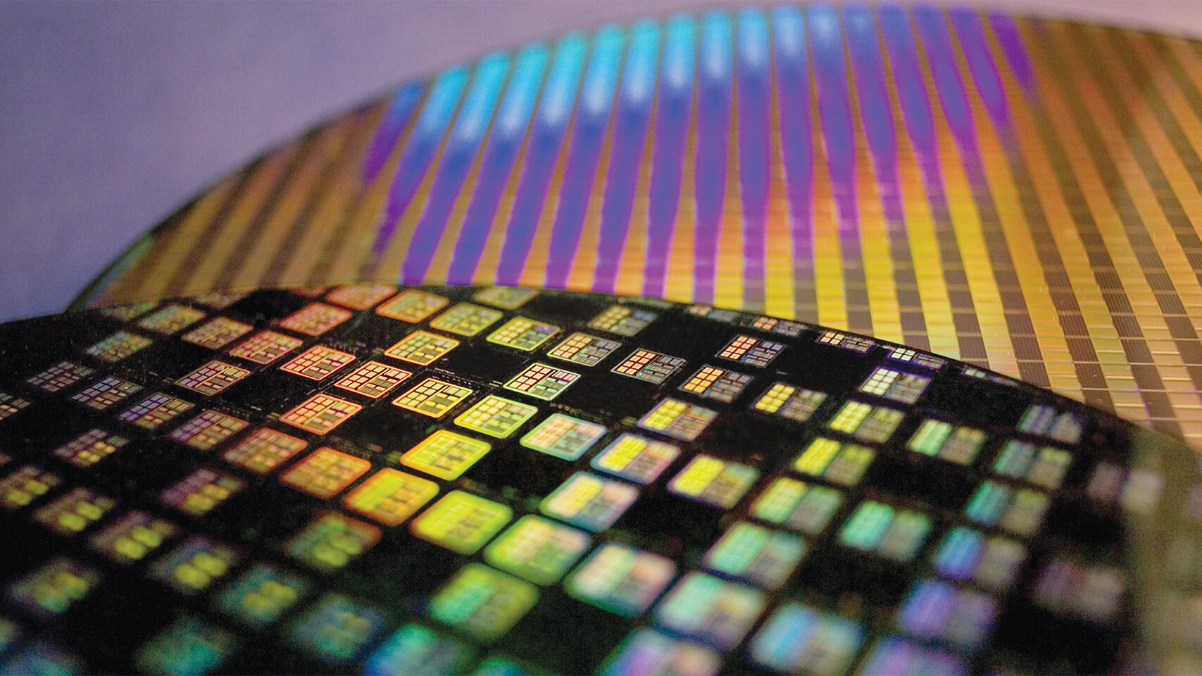
TSMC Expands Advanced Technology Leadership with N4P Process

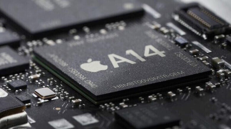
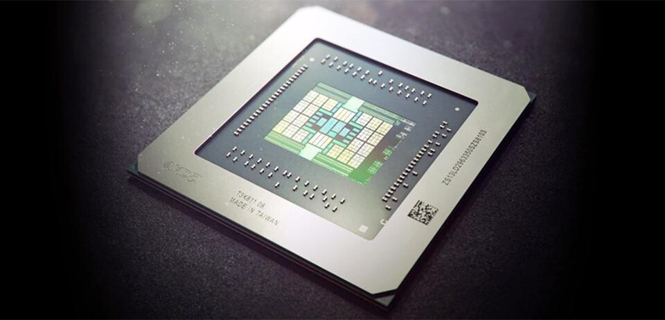
TSMC today introduced its N4P process, a performance-focused enhancement of the 5-nanometer technology platform. N4P joins the industry's most advanced and extensive portfolio of leading-edge technology processes. With N5, N4, N3 and the latest addition of N4P, TSMC customers will have multiple and compelling choices for power, performance, area, and cost for its products.

As the third major enhancement of TSMC's 5 nm family, N4P will deliver an 11% performance boost over the original N5 technology and a 6% boost over N4. Compared to N5, N4P will also deliver a 22% improvement in power efficiency as well as a 6% improvement in transistor density. In addition, N4P lowers process complexity and improves wafer cycle time by reducing the number of masks. N4P demonstrates TSMC's pursuit and investment in continuous improvement of our process technologies.

NVIDIA Rumored to Refresh RTX 30-series with SUPER SKUs in January, RTX 40-series in Q4-2022

NVIDIA is rumored to be giving its GeForce RTX 30-series "Ampere" graphics card family a mid-term refresh by the 2022 International CES, in January; the company is also targeting Q4-2022, specifically October, to debut its next-generation RTX 40-series. The Q1 refresh will include "SUPER" branded SKUs taking over key price-points for NVIDIA, as it lands up with enough silicon that can be fully unlocked. This leak comes from Greymon55, a reliable source on NVIDIA leaks. It also aligns with the most recent pattern followed by NVIDIA to keep its GeForce product-stack updated. The company had recently released "Ti" updates to certain higher-end price-points, in response to competition from the Radeon RX 6000 "RDNA2" series.

NVIDIA's next-generation will be powered by the "Lovelace" graphics architecture that sees even more hardware acceleration for the RTX feature-set, more raytraced effects, and preparation for future APIs. It also marks NVIDIA's return to TSMC, with the architecture reportedly being designed for the 5 nm (N5) silicon fabrication node. The current-gen GeForce "Ampere" chips are being products on an 8 nm foundry node by Samsung.

ASRock & NZXT Intel Z690, H670, B660, and H610 Motherboards Listed

The lineup of 600-Series motherboards planned by ASRock and NZXT for the upcoming 12th Generation Intel Core Series of processors has recently been published by VideoCardz. While NZXT has only two high-end Z590 motherboards listed with them being the N5-Z69XT, and the N7-Z69XT, ASRock has 36 listed across all the Z690, H670, B660, and H610 chipsets. The Z690 chipset will serve as the flagship platform for high-performance and overclocking while the H670 and B660 will take the mid-range and the H610 for entry-level boards. The list does not contain any Taichi, Aqua, or OC Formula series boards from ASRock as those may not be ready for day-one release or are still under active development.

ASRock will offer several of their motherboards in two variants with one offering integrated WiFi 6E networking, they also have an ITX option for each chipset. Intel is expected to announce their 12th Generation Core Series processors and Z690 chipset in late 2021 with the remaining chipsets to be announced at CES 2022. The entire list of motherboards from the two companies can be found below.

NVIDIA "Ada Lovelace" Architecture Designed for N5, GeForce Returns to TSMC

NVIDIA's upcoming "Ada Lovelace" architecture, both for compute and graphics, is reportedly being designed for the 5 nanometer silicon fabrication node by TSMC. This marks NVIDIA's return to the Taiwanese foundry after its brief excursion to Samsung, with the 8 nm "Ampere" graphics architecture. "Ampere" compute dies continue to be built on TSMC 7 nm nodes. NVIDIA is looking to double the compute performance on its next-generation GPUs, with throughput approaching 70 TFLOP/s, from a numeric near-doubling in CUDA cores, generation-over-generation. These will also be run at clock speeds above 2 GHz. One can expect "Ada Lovelace" only by 2022, as TSMC N5 matures.

Cadence Announces New Low-Power IP for PCI Express 5.0 Specification on TSMC N5 Process

Cadence Design Systems, Inc. (Nasdaq: CDNS) today announced immediate availability of Cadence IP supporting the PCI Express (PCIe ) 5.0 specification on TSMC N5 process technology. The next follow-on version on TSMC N3 process technology is expected to be taped out in early 2022. Collaboration with major customers is ongoing for N5 SoC designs targeting hyperscale computing and networking applications. The Cadence IP for PCIe 5.0 technology consists of a PHY, companion controller and Verification IP (VIP) targeted at SoC designs for very high-bandwidth hyperscale computing, networking and storage applications. With Cadence's PHY and Controller Subsystem for PCIe 5.0 architecture, customers can design extremely power-efficient SoCs with accelerated time to market.

The Cadence IP for PCIe 5.0 architecture offers a highly power-efficient implementation of the standard, with several evaluations from leading customers indicating it provides industry best-in-class power at the maximum data transfer rate of 32GT/s and worst-case insertion loss. Leveraging Cadence's existing N7/N6 silicon validated offering, the N5 design provides a full 512GT/s (gigatransfers per second) power-optimized solution across the full range of operating conditions with a single clock lane.

Apple M2 Processor is Reportedly in Mass Production

Apple's M1 processors are a big success. When Apple introduced the M1 processors in the MacBook lineup, everyone was impressed by the processor performance and the power efficiency it offered. Just a few days ago, Apple updated its Mac lineup to feature these M1 processors and made it obvious that custom silicon is the way to go in the future. Today, we have information coming from Nikkei Asia, that Apple's next-generation M2 chip has entered mass production and that it could be on the way for as early as July when Apple will reportedly refresh its products. The M2 chip is made inside TSMC's facilities on a 5 nm+ N5P node. While there is no more information coming from the report about the SoC, we can expect it to be a good generational improvement.

OpenFive Tapes Out SoC for Advanced HPC/AI Solutions on TSMC 5 nm Technology

OpenFive, a leading provider of customizable, silicon-focused solutions with differentiated IP, today announced the successful tape out of a high-performance SoC on TSMC's N5 process, with integrated IP solutions targeted for cutting edge High Performance Computing (HPC)/AI, networking, and storage solutions.

The SoC features an OpenFive High Bandwidth Memory (HBM3) IP subsystem and D2D I/Os, as well as a SiFive E76 32-bit CPU core. The HBM3 interface supports 7.2 Gbps speeds allowing high throughput memories to feed domain-specific accelerators in compute-intensive applications including HPC, AI, Networking, and Storage. OpenFive's low-power, low-latency, and highly scalable D2D interface technology allows for expanding compute performance by connecting multiple dice together using an organic substrate or a silicon interposer in a 2.5D package.

TSMC to Enter 4 nm Node Volume Production in Q4 of 2021

TSMC, the world leader in semiconductor manufacturing, has reportedly begun with plans to start volume production of the 4 nm node by the end of this year. According to the sources over at DigiTimes, Taiwan's leading semiconductor manufacturer could be on the verge of starting volume production of an even smaller node. The new 4 nm node is internally referred to as a part of the N5 node generation. The N5 generation covers N5 (regular 5 nm), N5P (5 nm+), and N4 process that is expected to debut soon. And perhaps the most interesting thing is that the 4 nm process will be in high-volume production in Q4, with Apple expected to be one of the major consumers of the N5 node family.

DigiTimes reports that Apple will use the N5P node for the upcoming Apple A15 SoCs for next-generation iPhones, while the more advanced N4 node will find itself as a base of the new Macs equipped with custom Apple Silicon SoCs. To find out more, we have to wait for the official product launches and see just how much improvement new nodes bring.

Apple A14 SoC Put Under the Microscope; Die Size, and Transistor Density Calculated

Apple has established itself as a master of silicon integrated circuit design and has proven over the years that its processors deliver the best results, generation after generation. If we take a look at the performance numbers of the latest A14 Bionic, you can conclude that its performance is now rivaling some of the x86_64 chips. So you would wonder, what is inside this SoC that makes it so fast? That is exactly what ICmasters, a semiconductor reverse engineering and IP services company, has questioned and decided to find out. For starters, we know that Apple manufactures the new SoCs on TSMC's N5 5 nm node. The Taiwanese company promises to pack 171.3 million transistors per square millimeter, so how does it compare to an actual product?

ICmasters have used electron microscopy to see what the chip is made out of and to measure the transistor density. According to this source, Apple has a chip with a die size of 88 mm², which packs 11.8 billion N5 transistors. The density metric, however, doesn't correspond to that of TSMC. Instead of 171.3 million transistors per mm², the ICmasters measured 134.09 million transistors per mm². This is quite a difference, however, it is worth noting that each design will have it different due to different logic and cache layout.
Apple A14 SoC Die Apple A14 SoC

TSMC 5 nm Node Supply Fully Booked, Apple the Biggest Customer

TSMC has hit a jackpot with its newer nodes like 7 nm and now 5 nm, as the company is working with quite good yields. To boast, TSMC has seen all of its capacity of 7 nm being fully booked by customers like AMD, Apple, and NVIDIA. However, it seems like the company's next-generation 5 nm node is also getting high demand. According to the latest report from DigiTimes, TSMC's N5 5 nm node is fully booked to the end of 2020. And the biggest reason for that is the biggest company in the world - Apple. Since Apple plans to launch the next-generation iPhone, iPad, and Arm-based MacBook, the company has reportedly booked most of the 5 nm capacity for 2020, meaning that there are lots of chips that Apple will consume. TSMC can't be dependent only on one company like Apple, so the smaller portion of capacity went to other customers as well.

Apple's Custom GPU is Reportedly Faster than Intel iGPU

When Apple announced their transition form Intel processors to Apple Silicon, we were left wondering how the silicon will perform and what characteristics will it bring with it. According to the latest report from The China Times, the Apple custom GPU found inside the new Apple Silicon will bring better performance and energy efficiency compared to Intel iGPU it replaces. The 5 nm GPU manufactured on TSMC's N5 semiconductor manufacturing node is supposedly codenamed "Lifuka" and it brings Apple's best to the table. Planned to power a 12-inch MacBook, the GPU will be paired with a custom CPU based on Arm ISA as well. The same chips powering iPhone and iPad devices will go into MacBook devices, with the TDP increased as MacBook will probably have much higher cooling capacity. The first Apple Silicon MacBook will come in H2 of 2021.
Here is the copy of a full report from The China Times below:

TSMC Details 3nm N3, 5nm N5, and 3DFabric Technology

TSMC on Monday kicked off a virtual tech symposium, where it announced its new 12 nm N12e node for IoT edge devices, announced the new 3DFabric Technology, and detailed progress on its upcoming 5 nm N5 and 3 nm N3 silicon fabrication nodes. The company maintains that the N5 (5 nm) node offers the benefits of a full node uplift over its current-gen N7 (7 nm), which recently clocked over 1 billion chips shipped. The N5 node incorporates EUV lithography more extensively than N6/N7+, and in comparison to N7 offers 30% better power at the same performance, 15% more performance at the same power, and an 80% increase in logic density. The company has commenced high-volume manufacturing on this node.

2021 will see the introduction and ramp-up of the N5P node, an enhancement of the 5 nm N5 node, offering a 10% improvement in power at the same performance, or 5% increase in performance at the same power. A nodelet of the N5 family of nodes, called N4, could see risk production in Q4 2021. The N4 node is advertised as "4 nm," although the company didn't get into its iso-power/iso-performance specifics over the N5 node. The next major node for TSMC will be the 3 nm N3 node, with massive 25%-30% improvement in power at the same performance, or 10%-15% improvement in performance at same power, compared to N5. It also offers a 70% logic density gain over N5. 3DFabric technology is a new umbrella term for TSMC's CoWoS (chip on wafer on substrate), CoW (chip on wafer), and WoW (wafer on wafer) 3-D packaging innovations, with which it plans to offer packaging innovations that compete with Intel's various new 3D chip packaging technologies on the anvil.

TSMC Planning a 4nm Node that goes Live in 2023

TSMC is reportedly planning a stopgap between its 5 nm-class silicon fabrication nodes, and the 3 nm-class, called N4. According to the foundry's CEO, Liu Deyin, speaking at a shareholders meeting, N4 will be a 4 nm node, and an enhancement of N5P, the company's most advanced 5 nm-class node. N4 is slated for mass-production of contracted products in 2023, and could help TSMC's customers execute their product roadmaps of the time. From the looks of it, N4 is a repeat of the N6 story: a nodelet that's an enhancement of N7+, the company's most advanced 7 nm-class node that leverages EUV lithography.

NVIDIA Underestimated AMD's Efficiency Gains from Tapping into TSMC 7nm: Report

A DigiTimes premium report, interpreted by Chiakokhua, aka Retired Engineer, chronicling NVIDIA's move to contract TSMC for 7 nm and 5 nm EUV nodes for GPU manufacturing, made a startling revelation about NVIDIA's recent foundry diversification moves. Back in July 2019, a leading Korean publication confirmed NVIDIA's decision to contract Samsung for its next-generation GPU manufacturing. This was a week before AMD announced its first new-generation 7 nm products built for the TSMC N7 node, "Navi" and "Zen 2." The DigiTimes report reveals that NVIDIA underestimated the efficiency gains AMD would yield from TSMC N7.

With NVIDIA's bonhomie with Samsung underway, and Apple transitioning to TSMC N5, AMD moved in to quickly grab 7 nm-class foundry allocation and gained prominence with the Taiwanese foundry. The report also calls out a possible strategic error on NVIDIA's part. Upon realizing the efficiency gains AMD managed, NVIDIA decided to bet on TSMC again (apparently without withdrawing from its partnership with Samsung), only to find that AMD had secured a big chunk of its nodal allocation needed to support its growth in the x86 processor and discrete GPU markets. NVIDIA has hence decided to leapfrog AMD by adapting its next-generation graphics architectures to TSMC's EUV nodes, namely the N7+ and N5. The report also speaks of NVIDIA using its Samsung foundry allocation as a bargaining chip in price negotiations with TSMC, but with limited success as TSMC established its 7 nm-class industry leadership. As it stands now, NVIDIA may manufacture its 7 nm-class and 5 nm-class GPUs on both TSMC and Samsung.

TSMC and Broadcom Enhance the CoWoS Platform with World's First 2X Reticle Size Interposer

TSMC today announced it has collaborated with Broadcom on enhancing the Chip-on-Wafer-on-Substrate (CoWoS ) platform to support the industry's first and largest 2X reticle size interposer. With an area of approximately 1,700mm2, this next generation CoWoS interposer technology significantly boosts computing power for advanced HPC systems by supporting more SoCs as well as being ready to support TSMC's next-generation five-nanometer (N5) process technology.

This new generation CoWoS technology can accommodate multiple logic system-on-chip (SoC) dies, and up to 6 cubes of high-bandwidth memory (HBM), offering as much as 96 GB of memory. It also provides bandwidth of up to 2.7 terabytes per second, 2.7 times faster than TSMC's previously offered CoWoS solution in 2016. With higher memory capacity and bandwidth, this CoWoS solution is well-suited for memory-intensive workloads such as deep learning, as well as workloads for 5G networking, power-efficient datacenters, and more. In addition to offering additional area to increase compute, I/O, and HBM integration, this enhanced CoWoS technology provides greater design flexibility and yield for complex ASIC designs in advanced process nodes.

TSMC: 5 nm on Track for Q2 2020 HVM, Ramping Faster than 7 nm

TSMC vice chairman and CEO C.C. Wei announced the company's plans for 5 nm are on track, which means High Volume manufacturing (HVM) on the node is expected to be achieved by 2Q 2020. The company has increased expenditures in ramping up its various nodes from an initially projected $10 billion to something along the lines of $14 billion - 15 billion; the company is really banking on quick uptake and design wins on its most modern process technologies - and the increased demand that follows.

TSMC's 5 nm process (N5) will use extreme ultraviolet lithography (EUVL) in many more layers than its N7+ and N6 processes, with up to 14 layers being etched in the N5 silicon compared to five and six, respectively, for its "older" N7+ and N6 processes. As the company increases capital expenditure in acquiring EUVL-capable equipment that sets up its production nodes for the market they foresee will just gobble up the chips in 2020, the company is optimistic they can achieve growth in the 5-10% number.
Return to Keyword Browsing
Apr 20th, 2025 02:58 EDT change timezone

New Forum Posts

Popular Reviews

Controversial News Posts