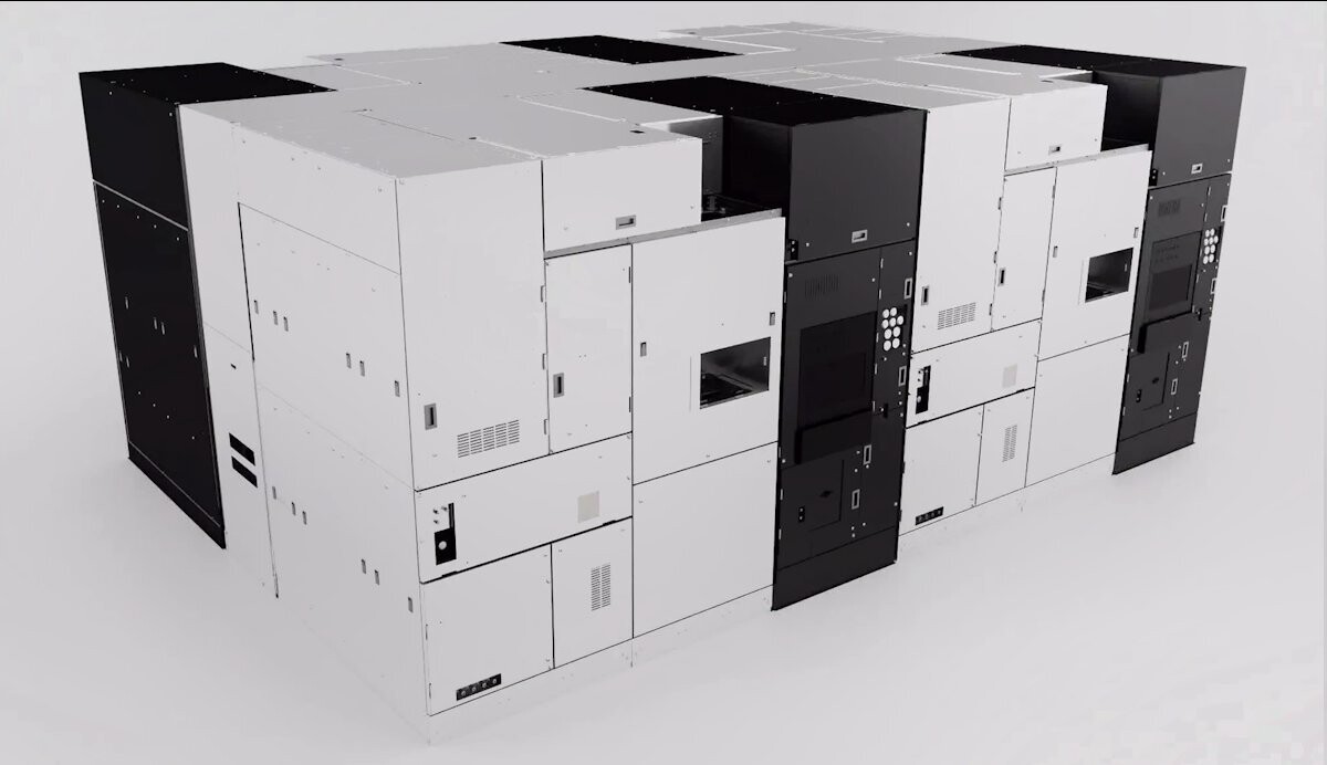
Canon Delivers FPA -1200NZ2C Nanoimprint Lithography System for Semiconductor Manufacturing to the Texas Institute for Electronics
Canon Inc. announced today that it will ship its most advanced lithography platform, the FPA-1200NZ2C nanoimprint lithography (NIL) system for semiconductor manufacturing, to the Texas Institute for Electronics (TIE), a Texas-based semiconductor consortium. Canon became the first in the world to commercialize a semiconductor manufacturing system that uses NIL technology, which forms circuit patterns in a different method from conventional projection exposure technology, when it released the FPA-1200NZ2C on October 13, 2023.
In contrast to conventional photolithography equipment, which transfers a circuit pattern by projecting it onto the resist coated wafer, the new product does it by pressing a mask imprinted with the circuit pattern into the resist on the wafer like a stamp. Because its circuit pattern transfer process does not go through an optical mechanism, fine circuit patterns on the mask can be faithfully reproduced on the wafer. With reduced power consumption and cost, the new system enables patterning with a minimum linewidth of 14 nm, equivalent to the 5 nm node that is required to produce most advanced logic semiconductors currently available.
In contrast to conventional photolithography equipment, which transfers a circuit pattern by projecting it onto the resist coated wafer, the new product does it by pressing a mask imprinted with the circuit pattern into the resist on the wafer like a stamp. Because its circuit pattern transfer process does not go through an optical mechanism, fine circuit patterns on the mask can be faithfully reproduced on the wafer. With reduced power consumption and cost, the new system enables patterning with a minimum linewidth of 14 nm, equivalent to the 5 nm node that is required to produce most advanced logic semiconductors currently available.