News Posts matching #Pascal

Return to Keyword Browsing

NVIDIA Unveils the Tesla P100 HPC Board based on "Pascal" Architecture

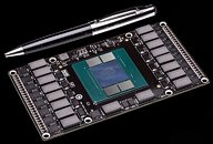
NVIDIA unveiled the Tesla P100, the first product based on the company's "Pascal" GPU architecture. At its core is a swanky new multi-chip module, similar in its essential layout to the AMD "Fiji." A 15 billion-transistor GPU die sits on top of a silicon wafer, through which a 4096-bit wide HBM2 memory interface wires it to four 3D HBM2 stacks; and with the wafer sitting on the fiberglass substrate that's rooted into the PCB over a ball-grid array. With the GPU die, wafer, and memory dies put together, this package has a cumulative transistor count of 150 billion transistors. The GPU die is built on the 16 nm FinFET process, and is 600 mm² in area.

The P100 sits on top of a space-efficient PCB that looks less like a video card, and more like a compact module that can be tucked away into ultra-high density supercomputing cluster boxes, such as the new NVIDIA DGX-1. The P100 offers a double-precision (FP64) compute performance of 5.3 TFLOP/s, FP32 performance of 10.6 TFLOP/s, and FP16 performance of a whopping 21.2 TFLOP/s. The chip has registers as big as 14.2 MB, and an L2 cache of 4 MB. In addition to PCI-Express, each P100 chip will be equipped with NVLink, and in-house developed high-bandwidth interconnect by NVIDIA, with bandwidths as high as 80 GB/s per direction, 160 GB/s both directions. This allows extremely high-bandwidth paths between GPUs, so they could share memory and work more like single-GPUs. The P100 is already in volume production, with its target customers already having bought it all the way up to its OEM channel availability some time in Q1-2017.


NVIDIA "GP104" Silicon to Feature GDDR5X Memory Interface

It looks like NVIDIA's next GPU architecture launch will play out much like its previous two generations - launching the second biggest chip first, as a well-priced "enthusiast" SKU that outperforms the previous-generation enthusiast product, and launching the biggest chip later, as the high-end enthusiast product. The second-biggest chip based on NVIDIA's upcoming "Pascal" architecture, the "GP104," which could let NVIDIA win crucial $550 and $350 price-points, will be a lean machine. NVIDIA will design the chip to keep manufacturing costs low enough to score big in price-performance, and a potential price-war with AMD.

As part of its efforts to keep GP104 as cost-effective as possible, NVIDIA could give exotic new tech such as HBM2 memory a skip, and go with GDDR5X. Implementing GDDR5X could be straightforward and cost-effective for NVIDIA, given that it's implemented the nearly-identical GDDR5 standard on three previous generations. The new standard will double densities, and one could expect NVIDIA to build its GP104-based products with 8 GB of standard memory amounts. GDDR5X breathed a new lease of life to GDDR5, which had seen its clock speeds plateau around 7 Gbps/pin. The new standard could come in speeds of up to 10 Gbps at first, and eventually 12 Gbps and 14 Gbps. NVIDIA could reserve HBM2 for its biggest "Pascal" chip, on which it could launch its next TITAN product.

NVIDIA GP100 Silicon to Feature 4 TFLOPs DPFP Performance

NVIDIA's upcoming flagship GPU based on its next-generation "Pascal" architecture, codenamed GP100, is shaping up to be a number-crunching monster. According to a leaked slide by an NVIDIA research fellow, the company is designing the chip to serve up double-precision floating-point (DPFP) performance as high as 4 TFLOP/s, a 3-fold increase from the 1.31 TFLOP/s offered by the Tesla K20, based on the "Kepler" GK110 silicon.

The same slide also reveals single-precision floating-point (SPFP) performance to be as high as 12 TFLOP/s, four times that of the GK110, and nearly double that of the GM200. The slide also appears to settle the speculation on whether GP100 will use stacked HBM2 memory, or GDDR5X. Given the 1 TB/s memory bandwidth mentioned on the slide, we're inclined to hand it to stacked HBM2.

TSMC Damaged by Earthquake, Could Impact AMD and NVIDIA GPU production

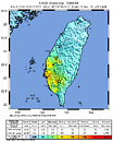
The recent 6.4 magnitude Taiwan earthquake, which hit the island nation on February 6th, affected TSMC worse than expected. Taiwan's premier semiconductor foundry, TSMC, had initially expected semiconductor wafer shipments to be down by less than 1%, but it is now emerging that the drop in shipments could be higher, because the damage to one of its facilities, Fab-14, is worse than originally assessed.

TSMC, in an official communication to its clients, assured that 95% of the foundry machines could return to functionality within 2-3 days after the earthquake. To that effect, machines in Fab-6 and Fab-14B have been fully restored. Despite the disaster, the company appears confident of reaching revenue targets of US $5.9-6.0 billion for Q1-2016. TSMC is the primary foundry partner of major fabless semiconductor companies, such as Qualcomm, NVIDIA, and AMD. AMD recently moved its next-generation GPU manufacturing to Korean silicon giant Samsung, while NVIDIA is building its next "Pascal" GPU family on TSMC's process.

NVIDIA Announces Drive PX 2 Mobile Supercomputer

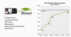
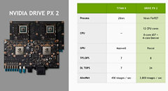
NVIDIA announced the Drive PX 2, the first in-car AI deep-learning device. This lunchbox sized "mobile supercomputer" embeds up to twelve CPU cores, a "Pascal" GPU built on the 16 nm FinFET process, 6 TFLOP/s of raw compute power, and 24 deep-learning TOps of compute power usable for deep-learning applications; the chips are liquid-cooled, draw 250W in all, and give the car a very powerful deep-learning device for self-driving cars. The device itself will be offered to car manufacturers to redesign and co-develop self-driving cars with.
The press-release follows.

Samsung to Fab AMD "Zen" and "Arctic Islands" on its 14 nm FinFET Node

It has been confirmed that Samsung will be AMD's foundry partner for its next generation GPUs. It has been reported that AMD's upcoming "Arctic Islands" family of GPUs could be built on the 14 nanometer FinFET LPP (low-power Plus) process. AMD's rival NVIDIA, meanwhile, is building its next-gen "Pascal" GPU family on 16 nanometer FinFET node, likely at its traditional foundry partner TSMC.

It gets better - not only will Samsung manufacture AMD's next-gen GPUs, but also its upcoming "Zen" family of CPUs, at least a portion of it. AMD is looking to distribute manufacturing loads between two foundries, Samsung and GlobalFoundries, perhaps to ensure that foundry-level teething trouble doesn't throw its product launch cycle off the rails. One of the most talked about "Arctic Islands" GPUs is codenamed "Greenland," likely a successor to "Fiji." Sales of some of the first chips - GPUs or CPUs - made at Samsung, will begin some time in Q3 2016. Some of the other clients for Samsung's 14 nm FinFET node are Apple and Qualcomm. The company plans to speed up development of its more advanced 10 nm node to some time in 2017.

NVIDIA GP100 Silicon Moves to Testing Phase

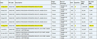
NVIDIA's next-generation flagship graphics processor, codenamed "GP100," has reportedly graduated to testing phase. That is when a limited batch of completed chips are sent from the foundry partner to NVIDIA for testing and evaluation. The chips tripped speed-traps on changeover airports, on their way to NVIDIA. 3DCenter.org predicts that the GP100, based on the company's "Pascal" GPU architecture, will feature no less than 17 billion transistors, and will be built on the 16 nm FinFET+ node at TSMC. The GP100 will feature an HBM2 memory interface. HBM2 allows you to cram up to 32 GB of memory. The flagship product based on GP100 could feature about 16 GB of memory. NVIDIA's design goal could be to squeeze out anywhere between 60-90% higher performance than the current-generation flagship GTX TITAN-X.

NVIDIA "Pascal" GPUs to be Built on 16 nm TSMC FinFET Node

NVIDIA's next-generation GPUs, based on the company's "Pascal" architecture, will be reportedly built on the 16 nanometer FinFET node at TSMC, and not the previously reported 14 nm FinFET node at Samsung. Talks of foundry partnership between NVIDIA and Samsung didn't succeed, and the GPU maker decided to revert to TSMC. The "Pascal" family of GPUs will see NVIDIA adopt HBM2 (high-bandwidth memory 2), with stacked DRAM chips sitting alongside the GPU die, on a multi-chip module, similar to AMD's pioneering "Fiji" GPU. Rival AMD, on the other hand, could build its next-generation GCNxt GPUs on 14 nm FinFET process being refined by GlobalFoundries.

Micron Begins Shipping its First 20 nm-class GDDR5 DRAM Chips

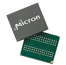
Micron Technology announced during its Q3 FY-2015 earnings call, that it began shipping GDDR5 memory chips based on its 20 nm-class node. The company is reportedly shipping 8 Gb (1 gigabyte) GDDR5 memory chips. The company was last reported to be acquiring Japanese DRAM major Elpida, which also supplies GDDR5 chips to graphics cards, notebooks, and game console makers. The GDDR5 memory space has been saturated by companies such as Samsung and SK Hynix. The memory standard itself is on the brink of becoming obsolete; with AMD implementing HBM on its new high-end GPU, and NVIDIA expected to implement HBM with its upcoming "Pascal" GPU family. There is still quite a few GDDR5-equipped graphics cards to be sold, before HBM takes over GPUs of all market segments.

NVIDIA Tapes Out "Pascal" Based GP100 Silicon

Sources tell 3DCenter.org that NVIDIA has successfully taped out its next big silicon based on its upcoming "Pascal" GPU architecture, codenamed GP100. A successor to GM200, this chip will be the precursor to several others based on this architecture. A tape-out means that the company has successfully made a tiny quantity of working prototypes for internal testing and further development. It's usually seen as a major milestone in a product development cycle.

With "Pascal," NVIDIA will pole-vault HBM1, which is making its debut with AMD's "Fiji" silicon; and jump straight to HBM2, which will allow SKU designers to cram up to 32 GB of video memory. 3DCenter.org speculates that GP100 could feature anywhere between 4,500 to 6,000 CUDA cores. The chip will be built on TSMC's upcoming 16 nanometer silicon fab process, which will finally hit the road by 2016. The GP100, and its companion performance-segment silicon, the GP104 (successor to GM204), are expected to launch between Q2 and Q3, 2016.
Return to Keyword Browsing
Nov 21st, 2024 10:25 EST change timezone

New Forum Posts

Popular Reviews

Controversial News Posts