News Posts matching #Pascal

Return to Keyword Browsing

NVIDIA Releases VRWorks SDK Update for "Pascal"

NVIDIA today released a major update to its VRWorks SDK that enables game developers to implement new VR features features introduced by the GeForce "Pascal" graphics processors, taking advantage of the new Simultaneous Multi-projection Engine (SMP). The two major features introduced are Lens-Matched Shading and Single-Pass Stereo.

Lens-Matched Shading uses SMP to provide substantial performance improvements in pixel shading. The feature improves upon Multi-res Shading by rendering to a surface that more closely approximates the lens corrected image that is output to the headset display. This avoids the performance cost of rendering many pixels that are discarded during the VR lens warp post-process. Single-Pass Stereo, on the other hand, removes the need for a GPU to render the geometry and tessellation of a 3D scene twice (one for each eye/viewport), and lets both viewports share one pass of geometry and tessellation, thereby halving the the tessellation and vertex-shading workload.

NVIDIA GeForce GTX 1080 Ti to be Based on GP102 Silicon

It looks like NVIDIA will have not one, but two "big chips" based on the "Pascal" architecture. The first one of course is the GP100, which made its debut with the Tesla P100 HPC processor. The GP100 is an expensive chip at the outset, featuring a combination of FP32 (single-precision) and FP64 (double-precision) CUDA cores, running up to 3,840 SPFP and 1,920 DPFP, working out to a gargantuan 5,760 CUDA core count. FP64 CUDA cores are practically useless on the consumer-graphics space, particularly in the hands of gamers. The GP100 also features a swanky 4096-bit HBM2 memory interface, with stacked memory dies sitting on the GPU package, making up an expensive multi-chip module. NVIDIA also doesn't want its product development cycle to be held hostage by HBM2 market availability and yields.

NVIDIA hence thinks there's room for a middle-ground between the super-complex GP100, and the rather simple GP104, if a price-war with AMD should make it impossible to sell a GP100-based SKU at $650-ish. Enter the GP102. This ASIC will be targeted at consumer graphics, making up GeForce GTX products, including the GTX 1080 Ti. It is cost-effective, in that it does away with the FP64 CUDA cores found on the GP100, retaining just a 3,840 FP32 CUDA cores count, 33% higher than that of the GP104, just as the GM200 had 33% more CUDA cores than the GM204.

ASUS Teases Upcoming G Series Notebooks Powered by "Pascal" GPUs

ASUS teased an upcoming Republic of Gamers G-Series notebook. It didn't stop at the teaser pics, and went on to tease performance numbers of the untitled "GXXX" graphics processor at the heart of this beast. We'll go out on a limb here and guess that it's a new mobile GPU based on the "Pascal" architecture; more so because ASUS is claiming that it's faster than even the desktop GeForce GTX TITAN X, and has 3DMark 11 Performance-present score to show for that. ASUS plans to exhibit the notebook at the 2016 Computex; and it's becoming increasingly clear that the third GP104-based SKU promised for June 2016 could be a mobile chip after all.

Colorful and Bykski Announce Liquid Cooling Ready GTX 1080 FE Bundle

Colorful and China-based liquid cooling components maker Bykski announced GeForce GTX 1080 Founders Edition graphics cards with bundled full-coverage water blocks, at a $100 premium (so that's a $100 premium over a $100 premium, over the $599 MSRP, totaling $799 for a card based on the second-biggest "Pascal" chip, kudos!). At this time, Colorful seems to be playing safe, and merely bundling the block with the card, so you could fit it yourself, just so it could get the bundle out on the shelves by May 27. In the near future (after NVIDIA has milked early adopters dry), Colorful could launch a "custom design" product (think of it as NVIDIA reference PCB with this block factory-fitted), which could likely lack the "Founders Edition" badge, and perhaps even be $100 cheaper.

NVIDIA GeForce GTX 1070 Clock Speeds Revealed

NVIDIA posted the product page of its upcoming GeForce GTX 1070 graphics card, confirming its clock-speeds, and related specifications. The card features a nominal GPU clock speed of 1506 MHz, with a maximum GPU Boost frequency of 1683 MHz. The memory is clocked at 2000 MHz (actual), or 8 GHz (GDDR5-effective), working out to a memory bandwidth of 256 GB/s. The company also rates the card's single-precision floating point performance at 6.45 TFLOP/s. Other key specs include 1,920 CUDA cores, 120 TMUs, and 64 ROPs. The GeForce GTX 1070 goes on sale, on the 10th of June, 2016.

NVIDIA GeForce GTX 1070 Specifications Revealed

NVIDIA's second graphics card based on its GP104 "Pascal" silicon, the more affordable GeForce GTX 1070, hits the shelves on June 10, 2016. At the May 7th event, the company was surprisingly quiet about its specifications, until now. It turns out that slower memory isn't the only thing setting the GTX 1070 apart from the GTX 1080. The company will also cut down the CUDA core count, a proportionate number of TMU count, and lower the GPU clock speeds.

NVIDIA set the MSRP for the GeForce GTX 1070 at US $379, $50 higher than the launch-price of the GTX 970, the most popular SKU based on the GM204 silicon. The company also plans to sell a premium reference-design card, dubbed the GeForce GTX 1070 Founders Edition, at $449, at a $70 premium. NVIDIA hopes to make the GTX 1070 the go-to card for Summer 2016 PC upgrades.
The specifications follow.

Colorful Releases its GeForce GTX 1080 Founders Edition Graphics Card

Colorful Technology Company Limited,professional manufacturer of graphics cards and motherboards, proudly debuts the world's first GeForce GTX 1080 graphics card. Announced May 6th, the new GeForce GTX 1080 will feature NVIDIA's latest GPU architecture codenamed Pascal boasting a 16nm FinFET fabrication process.

The GeForce GTX 1080 is based on the GP104 GPU armed with 2560 CUDA cores and will have a base engine clock of 1607 MHz and can boost up 1733 MHz. Complementing it will be 8 GB of GDDR5X video memory running at an effective clock rate of 10 GHz on a 256-bit bus. The GeForce GTX 1080 is designed to deliver 3x more performance than previous-generation graphics card and its breakthrough innovations in gaming give gamers new possibilities to enjoy via VR experiences.

NVIDIA Announces Financial Results for First Quarter Fiscal 2017

NVIDIA today reported revenue for the first quarter ended May 1, 2016, of $1.30 billion, up 13 percent from $1.15 billion a year earlier, and down 7 percent from $1.40 billion in the previous quarter. GAAP earnings per diluted share for the quarter were $0.33, up 38 percent from $0.24 a year ago and down 6 percent from $0.35 in the previous quarter. Non-GAAP earnings per diluted share were $0.46, up 39 percent from $0.33 a year earlier and down 12 percent from $0.52 in the previous quarter.

"We are enjoying growth in all of our platforms -- gaming, professional visualization, datacenter and auto," said Jen-Hsun Huang, co-founder and chief executive officer, NVIDIA. "Accelerating our growth is deep learning, a new computing model that uses the GPU's massive computing power to learn artificial intelligence algorithms. Its adoption is sweeping one industry after another, driving demand for our GPUs.

NVIDIA to Focus on 2-way SLI with GeForce "Pascal"

At its GeForce GTX 1080 launch event, NVIDIA is said to have told the press that with its GeForce "Pascal" series, the company will focus on 2-way SLI "for maximum performance," implying an uncertain future for 3-way and 4-way SLI. The company's new SLI HB bridge introduced with the GTX 1080, enables higher bandwidth between two graphics cards in SLI, letting them more reliably render games at high resolutions. On the downside, this new bridge occupies both SLI contact points on each card, in 2-way SLI.

It might still be possible to do 3-way and 4-way SLI using a classic 3-way or 4-way bridge included with your motherboard. You'd be at the mercy of applications somehow being able to take advantage of 3-4 GPUs, NVIDIA on its part, will likely only optimize its drivers for 2-way SLI. The knight in shining armour here is DirectX 12 native multi-GPU, which doesn't care how many GPUs you're using, or if they're even the same kind (as long as the GPUs and the app support Direct3D 12).

NVIDIA GeForce GTX 1080 Specifications Released

After launching its shockingly fast (claimed) GeForce GTX 1080 and GTX 1070 graphics cards, NVIDIA posted specifications of the former. The two are based on NVIDIA's swanky new 16 nm "GP104" silicon, derived from its "Pascal" GPU architecture. The architecture is detailed in our older article, here. The GeForce GTX 1080 leads the pack, featuring four graphics processing clusters, holding 2,560 CUDA cores. The core runs at a scorching 1607 MHz, with a GPU Boost frequency of 1733 MHz. In one of its demos, NVIDIA overclocked this chip to over 2100 MHz, on its reference air cooling, and the GPU barely scraped 67 °C under stress. The GTX 1080 features a 256-bit wide GDDR5X memory interface, holding 8 GB of memory. The memory is clocked at 2500 MHz (10 GHz effective), working out to a memory bandwidth of 320 GB/s.

API support includes DirectX 12 (feature-level 12_1), OpenGL 4.5, and Vulkan. Display outputs include three DisplayPort 1.4 connectors, one HDMI 2.0b, and one dual-link DVI. The reference-design card is 10.5-inch long, and double-slot. It draws power from a single 8-pin PCIe power connector, and its typical board power is rated at 180W. With the GeForce "Pascal" family, instead of caving in to DirectX 12 native multi-GPU, NVIDIA developed its SLI technology further, with the new SLI HB (high-bandwidth) bridge standard. It's essentially a 2-way bridge in which both SLI fingers of the card are used. This doubles bandwidth between the two cards, allowing higher display resolutions, and multi-display setups between high-resolution monitors. The GeForce GTX 1080 will be available from May 27, 2016, starting at US $599. The $379 GTX 1070 specifications will be revealed closer to its June 10, 2016 market availability.

NVIDIA Announces the GeForce GTX 1080, Faster than GTX 980 SLI

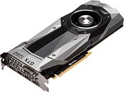
NVIDIA announced its next-generation GeForce GTX 1080 graphics card. Based on the "Pascal" architecture, this chip is built on the 16 nm FinFET process. It uses GDDR5X memory at 10 GHz (GDDR5-effective) clock speed. NVIDIA announced major improvements to the VRM that drives graphics cards, that increases switching efficiency. NVIDIA announced that the GeForce GTX 1080 is faster than a GeForce GTX 980 SLI, and a GeForce GTX TITAN X. The air-cooled GTX 1080 runs at a very high clock speed or 2.11 GHz, with 10 GHz memory clocks, at a temperature of 67 degrees C. Available on May 27, it's priced at $599.
More pictures after the break.

NVIDIA New GTX 1080 Cooler Shroud Design Confirmed

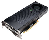
It looks like the over-the-top, edgy design of the reference-design cooler of NVIDIA's GeForce GTX 1080 and GTX 1070 graphics cards, which was extensively pictured, is real. Pictures of the aluminium cooler shroud first surfaced in April, when a CNC mill worker leaked pictures of two cooler shrouds fresh out of a machine. A render of this design formed the background image of GeForce website since its most recent update, announcing today's Livestream of the NVIDIA GeForce "Pascal" launch event.

NVIDIA Teases "Pascal" Launch with "Order of 10" Puzzle

NVIDIA just sent reviewers a curious looking briefcase with pieces to an elaborate puzzle under the ominous-sounding Order of 10 website. Besides the puzzle, the site has a countdown that ends on 6th May 2016. The solution to the "Order of 10" puzzle, along with several other highlights, such as a Battlefield 5 reveal, could form highlights of NVIDIA's GeForce GTX 10-series graphics cards. The company plans to unveil its next-generation "Pascal" architecture-based GeForce GPUs, beginning with the GeForce GTX 1080, and the GTX 1070, as early as on 6th May, with reviews and market-availability slated for early-June.

NVIDIA to Unveil GeForce GTX 1080 and GTX 1070 This Week

That's right, the launch (or at least unveiling) of NVIDIA's next-generation "Pascal" architecture based GeForce GTX 1080 and GTX 1070 could be a lot sooner than the "early-June" date making rounds. According to sources with an invite to an event in Austin, Texas; NVIDIA could talk the money-making end of the "Pascal" architecture (GeForce products), on May 6th.

This is when NVIDIA will give the GTX 1080 and GTX 1070 at least a paper-launch. Availability of add-in card (AIC) partner branded cards, as well as reviews of the two cards, could still be slated for early-June. What's more, EA-DICE' "Battlefield 5" (working title) unveiling is scheduled around the same time. Could it be that NVIDIA could pull off something big? Think Battlefield 5 at 4K, with a single card?

New GP104 ASIC Picture Hints at GTX 1080 with GDDR5X Memory

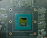
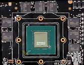
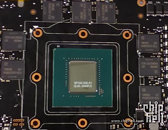
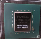
A new picture of NVIDIA GP104 "Pascal" ASIC surrounded with GDDR5X memory chips hints at the possibility of NVIDIA reserving the new fast memory standard for the GTX 1080, and older GDDR5 for the more affordable GTX 1070. The picture reveals a GP104 chip with the ASIC code "GP104-400-A1," surrounded by eight Micron-made GDDR5X memory chips. We know from an older article that this ASIC code denotes the top-tier GTX 1080. A second picture (recently posted) reveals a "GP104-200-A1" ASIC surrounded by conventional GDDR5 memory chips. This ASIC corresponds to the second-fastest GTX 1070.

GDDR5 and GDDR5X are nearly identical electrically, and it's quite conceivable that the GP104 chip features a memory controller that supports both standards. GDDR5 can be had at speeds of up to 8 Gbps, while GDDR5X chips can range between 10 Gbps thru 12 Gbps initially, with 14 Gbps chips planned for a little later. Besides memory, CUDA core count could be another factor that sets the two SKUs apart. NVIDIA is planning to launch a total of three SKUs based on the GP104 silicon, in June 2016, beginning with the GTX 1080 and GTX 1070 in early-June (probably along the sidelines of Computex 2016), and a third SKU in mid-June.

NVIDIA GP104 "Pascal" ASIC Pictured

Here are two of the first pictures of NVIDIA's upcoming "GP104" graphics processor. This chip will drive at least three new GeForce SKUs bound for a June 2016 launch; and succeeds the GM204 silicon, which drives the current-gen GTX 980 and GTX 970. Based on the "Pascal" architecture, the GPU will be built on TSMC's latest 16 nm FinFET+ node. The chip appears to feature a 256-bit wide GDDR5 memory interface, and is rumored to feature a memory clock of 8 Gbps, yielding a memory bandwidth of 256 GB/s.

NVIDIA to Launch Mid-range GP106 Based Graphics Cards in Autumn 2016

NVIDIA is expected to launch the first consumer graphics cards based on the GP106 silicon some time in Autumn 2016 (late Q3-early Q4). Based on the company's next-generation "Pascal" architecture, the GP106 will drive several key mid-range and performance-segment (price/performance sweetspot) SKUs, including the cards that succeed the current GeForce GTX 960 and GTX 950. Based on the way NVIDIA's big GP100 silicon is structured, assuming the GP106 features two graphics processing clusters (GPCs), the way the current GM206 silicon does; one can expect a CUDA core count in the neighborhood of 1,280. NVIDIA could use this chip to capture several key sub-$250 price points.

NVIDIA Reportedly Stops Production of Certain "Maxwell" GPUs

Paving the way for its next-generation "Pascal" architecture-based performance-thru-enthusiast GPUs, NVIDIA reportedly halted further production of certain current-generation "Maxwell" GPUs. HWBattle reports that production of the GM204-based GeForce GTX 980, the popular GTX 970, and GM200-based GTX 980 Ti have seen production halts, to let the market digest existing inventories of the three cards; and letting NVIDIA's add-in card (AIC) partners prepare to stock up next-generation graphics cards, beginning with at least three SKUs based on the GP104 silicon, in June 2016.

NVIDIA Readies Three GP104 "Pascal" Based SKUs for June 2016

NVIDIA is reportedly giving final touches to no less than three SKUs based on the 16 nm GP104 silicon, to launch some time this June. The ASIC markings for the chips that drive these SKUs are "GP104-400-A1," "GP104-200-A1" and "GP104-150-A1." If you recall, NVIDIA last reserved the "-400-A1" markings for the GeForce GTX 980 (GM204-400-A1), and the "-200-A1" for the GTX 970 (GM204-200-A1).

The GP104-150-A1 is a mystery ASIC. Either it will drive a more affordable third desktop SKU based on the GP104, or could signify a mobile SKU. The company plans to launch the products based on the GP104-400-A1 and GP104-200-A1, logical successors to the GeForce GTX 980 and GTX 970, in early June. The GP104-150-A1, on the other hand, could see the light of the day in mid-June.

NVIDIA "Pascal" GP100 Silicon Detailed

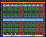
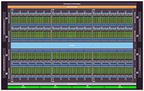
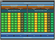
The upcoming "Pascal" GPU architecture from NVIDIA is shaping up to be a pixel-crunching monstrosity. Introduced as more of a number-cruncher in its Tesla P100 unveil at GTC 2016, we got our hands on the block diagram of the "GP100" silicon which drives it. To begin with, the GP100 is a multi-chip module, much like AMD's "Fiji," consisting of a large GPU die, four memory-stacks, and silicon wafer (interposer) acting as substrate for the GPU and memory stacks, letting NVIDIA drive microscopic wires between the two. The GP100 features a 4096-bit wide HBM2 memory interface, with typical memory bandwidths of up to 1 TB/s. On the P100, the memory ticks at 720 GB/s.

At its most top-level hierarchy, the GP100 is structured much like other NVIDIA GPUs, with the exception of two key interfaces - bus and memory. A PCI-Express gen 3.0 x16 host interface connects the GPU to your system, the GigaThread Engine distributes workload between six graphics processing clusters (GPCs). Eight memory controllers make up the 4096-bit wide HBM2 memory interface, and a new "High-speed Hub" component, wires out four NVLink ports. At this point it's not known if each port has a throughput of 80 GB/s (per-direction), or all four ports put together.
First NVIDIA "Pascal" Graphics Cards to be Unveiled at Computex 2016

Some of the first consumer graphics cards based on NVIDIA's next-generation "Pascal" architecture, could debut at Computex 2016 (late-May thru early-June), with mass shipments some time in July, 2016, according to Taiwan-based industry observer DigiTimes. NVIDIA plans to unveil the "GeForce GTX 1080" and "GTX 1070" through its add-in card (AIC) partners, with Taiwan-based companies such as ASUS, MSI, and GIGABYTE, planning to showcase their graphics cards at the event.

It looks like the company could allow non-reference board designs at launch, although pictures of reference-design cooler shrouds, allegedly from an aluminium CNC mill, have been making rounds on the web. Along with AMD's "Polaris," NVIDIA "Pascal" is the first GPU architecture to launch post-Windows 10, and the DirectX 12 API it introduced.

NVIDIA "Pascal" GP104 Silicon Pictured

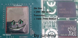
A picture of NVIDIA's next performance-segment GPU based on the upcoming "Pascal" architecture, the GP104, was leaked to the web, revealing a heap of raw material to speculate from. To begin with, GP104 retains the traditional component layout of a simple GPU die sitting on a conventional fiberglass substrate package, with memory chips surrounding it. NVIDIA is reserving exotic specs such as stacked HBM2 memory for the high-end GP100 silicon.

Some fairly straightforward trignometry reveals that the rectangular die of the GP104 measures 15.35 mm x 19.18 mm, with one source speculating a transistor-count of 7.4-7.9 billion. The card is expected to feature 8 gigabit GDDR5 memory chips, which tick at 8 GHz (GDDR5-effective). If the memory bus width is 256-bit, then you're looking at a memory bandwidth of 256 GB/s. The CUDA core count of the GP104 could be closer to 2,560, than the 4,096 from an older report.

NVIDIA Launches World's First Deep Learning Supercomputer

NVIDIA today unveiled the NVIDIA DGX-1, the world's first deep learning supercomputer to meet the unlimited computing demands of artificial intelligence. The NVIDIA DGX-1 is the first system designed specifically for deep learning -- it comes fully integrated with hardware, deep learning software and development tools for quick, easy deployment. It is a turnkey system that contains a new generation of GPU accelerators, delivering the equivalent throughput of 250 x86 servers.

The DGX-1 deep learning system enables researchers and data scientists to easily harness the power of GPU-accelerated computing to create a new class of intelligent machines that learn, see and perceive the world as humans do. It delivers unprecedented levels of computing power to drive next-generation AI applications, allowing researchers to dramatically reduce the time to train larger, more sophisticated deep neural networks.

Mid-range "Pascal" GPUs Stick to GDDR5-class Memory

At the NVIDIA Drive PX compute module unveiling, company CEO Jen-Hsun Huang gave us the first glimpse of a mid-range GPU based on the "Pascal" architecture. This chip looks a lot more conventional than the fancy HBM2-infused multi-chip module that's at the heart of the Tesla P100. Its package is a traditional green fiberglass substrate with a rectangular die at the center; and is surrounded by conventional-looking GDDR5-class memory chips (which could very well be GDDR5X). The Drive PX is a GPU-accelerated deep-learning box that NVIDIA is basing much of its self-driving car tech around; and uses a pair of these mid-range "Pascal" MXM boards.
Return to Keyword Browsing
Nov 21st, 2024 10:38 EST change timezone

New Forum Posts

Popular Reviews

Controversial News Posts