Saturday, May 7th 2016

NVIDIA GeForce GTX 1080 Specifications Released
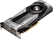
After launching its shockingly fast (claimed) GeForce GTX 1080 and GTX 1070 graphics cards, NVIDIA posted specifications of the former. The two are based on NVIDIA's swanky new 16 nm "GP104" silicon, derived from its "Pascal" GPU architecture. The architecture is detailed in our older article, here. The GeForce GTX 1080 leads the pack, featuring four graphics processing clusters, holding 2,560 CUDA cores. The core runs at a scorching 1607 MHz, with a GPU Boost frequency of 1733 MHz. In one of its demos, NVIDIA overclocked this chip to over 2100 MHz, on its reference air cooling, and the GPU barely scraped 67 °C under stress. The GTX 1080 features a 256-bit wide GDDR5X memory interface, holding 8 GB of memory. The memory is clocked at 2500 MHz (10 GHz effective), working out to a memory bandwidth of 320 GB/s.
API support includes DirectX 12 (feature-level 12_1), OpenGL 4.5, and Vulkan. Display outputs include three DisplayPort 1.4 connectors, one HDMI 2.0b, and one dual-link DVI. The reference-design card is 10.5-inch long, and double-slot. It draws power from a single 8-pin PCIe power connector, and its typical board power is rated at 180W. With the GeForce "Pascal" family, instead of caving in to DirectX 12 native multi-GPU, NVIDIA developed its SLI technology further, with the new SLI HB (high-bandwidth) bridge standard. It's essentially a 2-way bridge in which both SLI fingers of the card are used. This doubles bandwidth between the two cards, allowing higher display resolutions, and multi-display setups between high-resolution monitors. The GeForce GTX 1080 will be available from May 27, 2016, starting at US $599. The $379 GTX 1070 specifications will be revealed closer to its June 10, 2016 market availability.
API support includes DirectX 12 (feature-level 12_1), OpenGL 4.5, and Vulkan. Display outputs include three DisplayPort 1.4 connectors, one HDMI 2.0b, and one dual-link DVI. The reference-design card is 10.5-inch long, and double-slot. It draws power from a single 8-pin PCIe power connector, and its typical board power is rated at 180W. With the GeForce "Pascal" family, instead of caving in to DirectX 12 native multi-GPU, NVIDIA developed its SLI technology further, with the new SLI HB (high-bandwidth) bridge standard. It's essentially a 2-way bridge in which both SLI fingers of the card are used. This doubles bandwidth between the two cards, allowing higher display resolutions, and multi-display setups between high-resolution monitors. The GeForce GTX 1080 will be available from May 27, 2016, starting at US $599. The $379 GTX 1070 specifications will be revealed closer to its June 10, 2016 market availability.

103 Comments on NVIDIA GeForce GTX 1080 Specifications Released
If you read the fine print. Its not DP 1.4 connectors they are DP 1.2 with DP 1.3 & 1.4 ready. They don't support some features I'm guessingOn the bright side its has HDMI 2.0b. It should be able to take advantage of HDMI version of DisplayPorts adaptive-sync (dynamic-sync) if Nvidia chooses to do so.
Tbh, I didn't catch that until the third time I read the news myself.
The laptop panels are not special and have nothing added to them. They're just eDP.
Deal with it. Nvidia is not your pal.
I can afford it, but can't justify buying it. (mid range card, FFS)
Yet, this might be a very good strategy for nVidia. I see hype everywhere.
1080 will likely create great halo effect. (it already does, despite lack of any real world benchmarks whatsoever)
AMD, judging from its Polaris 10 GPU size, can not compete vs these perf wise.
1070 specs are yet to be defined, apparently, waiting for AMD release, poised to spoil it.
Now, AMD's "we wanna go multi" approach might make perfect sense (better yelds, console like etc) but I don't see how it could help here and now.
So, so far no signs of AMD recovering even a bit (count me into pessimists) too bad for consumers. I wish I was wrong.
Cause 8Gb is such a big increase, over what, say, 390 has. Oh wait...
The cost per wafer (once yields are on par with 28nm) isn't prohibitively larger ($4800 per 16nmFF+ wafer vs $3500 for 28nm) which would only add around $4 per GPU - assuming the 333mm² (1:1.25 die ratio, 16.33mm * 20.4mm size) is accurate....but that is also assuming yields would be the same between a very mature 28nm process and a very immature 16nmFF+ process.....Which I highly doubt is the case at present.
The other major contributer would be overall chip design cost for a chip with a much higher transistor density and a couple of extra metal layers (at least):Comparing two chips made on two different process nodes - one very mature, one very immature - of vastly different complexity, and trying to justify the same end user cost is an exercise in futility. I doubt the BoM of the assembled cards differs too greatly, although 8Gbps GDDR5 IC's would carry a reasonable price premium over 7Gbps chips of half the density (4Gb rather than 8Gb for the GTX 1070).