 301
301
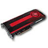
AMD Radeon HD 7970 3 GB Review
(301 Comments) »Introduction
Out with the old, in with the new. Let's welcome the newest kid on the block, the Radeon HD 7970, part of AMD's spanking new Southern Islands GPU family. This card is the industry's first with a few things, it uses the first ever high-performance GPU built on the 28 nanometer silicon fabrication process; Radeon HD 7970 is the industry's first card compliant with Microsoft's DirectX 11.1 API, which will ship with the next major version of Windows; and is the first card to use the PCI Express 3.0 x16 bus, that doubles system interface bandwidth to 32 Gb/s and is touted by motherboard manufacturers as the next big thing since PCI.
New generations of GPUs naturally bring with them performance increments, some times even 100% that of preceding generations, they also serve as launch-vehicles for new features that quickly go on to become industry standards, and help the technology grow. The Radeon HD 7970 has both of these responsibilities resting on its shoulders: to score performance wins, and pack some killer new features that matter to the end-user.

Product Positioning
The AMD Radeon HD 7970 is a unique card from a market-positioning standpoint. After Radeon HD 2900 series, and the completion of ATI's merger with AMD, the company took up a unique model of product development that ensured it could have competitive products out in the market targeting every segment, while not having to spend much on making large GPUs. Its goal with a new GPU architecture always involved making a killer high-performance (not high-end) GPU, and using it both ways: in dual-GPU cards as high-end products, and by disabling some components/features to carve out cheaper/cost-effective products.The AMD Radeon HD 7970, particularly the GPU behind it, codenamed "Tahiti", is stretching that model a little towards the higher-end. Tahiti is bigger than what AMD's typical "high-performance" GPU is supposed to be. For one, it features a 384-bit wide memory interface. AMD was the first to market with GDDR5 memory standard, which it initially sought as a way to circumvent the need for a GDDR3/4 memory bus wider than 256-bits. With NVIDIA catching up with the memory standard, and implementing a 384-bit GDDR5 memory interface on its GeForce Fermi 100/110 GPUs, AMD felt the pinch for doing something to increase the memory bandwidth of the HD 7970, to keep up with the increasing compute performance of their GPUs. The company chose slightly faster GDDR5 memory chips with HD 6900 series, but it could only yield small bandwidth gains. The only option left without having to switch memory architecture to the lesser known XDR2, was to increase the memory bus width physically by 50%, hence 384-bit. Coupled with the faster 5.5 GT/s memory chips it used on the HD 6900, and appropriate clock speeds, it yields around 260 GB/s of memory bandwidth.

The unconventionally-wider memory bus of the Radeon HD 7970, combined with a brand new math-processing machinery contribute to the HD 7970's product placement, which is between the previous-generation single-GPU Radeon HD 6970, and previous-generation dual-GPU HD 6990, tilting closer towards the HD 6990.
| GeForce GTX 560 | GeForce GTX 560 Ti | GeForce GTX 560 Ti 448 C | Radeon HD 6950 | GeForce GTX 570 | Radeon HD 6970 | GeForce GTX 580 | Radeon HD 7970 | Radeon HD 6990 | GeForce GTX 590 | ||
|---|---|---|---|---|---|---|---|---|---|---|---|
| Shader Units | 336 | 384 | 448 | 1408 | 480 | 1536 | 512 | 2048 | 2x 1536 | 2x 512 | |
| ROPs | 32 | 32 | 40 | 32 | 40 | 32 | 48 | 32 | 2x 32 | 2x 48 | |
| Graphics Processor | GF114 | GF114 | GF110 | Cayman | GF110 | Cayman | GF110 | Tahiti | 2x Cayman | 2x GF110 | |
| Transistors | 1950M | 1950M | 3000M | 2640M | 3000M | 2640M | 3000M | 4310M | 2x 2640M | 2x 3000M | |
| Memory Size | 1024 MB | 1024 MB | 1280 MB | 2048 MB | 1280 MB | 2048 MB | 1536 MB | 3072 MB | 2x 2048 MB | 2x 1536 MB | |
| Memory Bus Width | 256 bit | 256 bit | 320 bit | 256 bit | 320 bit | 256 bit | 384 bit | 384 bit | 2x 256 bit | 2x 384 bit | |
| Core Clock | 810 MHz | 823 MHz | 732 MHz | 800 MHz | 732 MHz | 880 MHz | 772 MHz | 925 MHz | 830 MHz | 607 MHz | |
| Memory Clock | 1002 MHz | 1002 MHz | 950 MHz | 1250 MHz | 950 MHz | 1375 MHz | 1002 MHz | 1375 MHz | 1250 MHz | 855 MHz | |
| Price | $180 | $210 | $290 | $250 | $330 | $340 | $500 | $549 | $700 | $750 |
Architecture

Tahiti, named after the lovely Tahiti islands of French Polynesia in the South Pacific, is AMD's new high-performance GPU. It succeeds Cayman, the chip powering the Radeon HD 6900 series and the dual-GPU HD 6990. Tahiti is built on TSMC's brand new 28 nanometer silicon fabrication process. In a nutshell, it retains the tried and trusted component hierarchy of its predecessors, but with major changes in the math processing SIMD machinery, and raster operations processors (ROPs) de-linked from the memory bus width.

With Tahiti, AMD is introducing the biggest revamp in the way its GPUs crunch numbers, since the Radeon HD 2000. Back then AMD adopted the "Graphics Parallel Core" compute architecture which uses clumps of super-scalar processors that work out "very long instruction words" (VLIW). The older version of Graphics Parallel Core used sets of four simple stream processors with one complex stream processor (that has more capabilities), along with branch units and general purpose registers. This made up with VLIW5 design. With Radeon HD 6900 "Cayman" GPU, AMD implemented a newer design that used groups of four equipotent stream processors, making up the more advanced VLIW4 design.


As mentioned earlier, for the most part, the GPU's component hierarchy is the same, except that its number-crunching parts have undergone, in AMD's words, a revolutionary change. VLIW5 to VLIW4 was evolutionary, in comparison. With Tahiti, AMD replaced its VLIW stream processor clusters with GCN (Graphics Core Next) compute units. Each GCN compute unit is a super-scalar processor that combines scalar and vector elements that follow a new non-VLIW instruction-set architecture, and utilizes an improved layout of shared and dedicated components. To the end-user, this architecture translates into higher performance per millimeter square of GPU die area. Smaller the GPU die, cheaper it is to produce, and sometimes, lower its power draw.


Graphics CoreNext also brings with it what AMD refers to as its 9th Generation Tessellation unit. Tahiti packs two geometry engines, and with it, two independent tessellation units. These units take advantage of larger parameter caches, new off-chip buffering capabilities, and new vertex reuse instructions to deliver a whopping four times tessellation performance improvement over the previous generation, at least on paper.

In a nutshell, the Tahiti die measures 365 mm², holding 4.31 billion transistors. It is built on the 28 nm TSMC process. It has 32 GCN compute units and 2048 stream processors in all. There are 128 texture memory units (TMUs), and 32 raster operation processors (ROPs). Despite having a 384-bit wide memory interface, the raster operations processor (ROP) count didn't increase proportionately to 48, as expected. This is because AMD reconfigured the way ROPs interact with the rest of the GPU, and hence retained its conventional ROP count of 32. The 384-bit wide memory interface combined with 5.5 GT/s GDDR5 memory chips sums up to a 264 GB/s memory bandwidth. Since it uses twelve 2 Gbit memory chips, it ends up with 3 GB of total memory on board.
Packaging & Contents
We received a card only from AMD, without packaging but rest assured, the retail units will come with standard accessories like adapters and power cables.With the Radeon HD 7970 AMD requires all partners to bundle an HDMI to (single link) DVI adapter, so that you can use the card with two DVI monitors.
Our Patreon Silver Supporters can read articles in single-page format.
Apr 12th, 2025 02:24 EDT
change timezone
Latest GPU Drivers
New Forum Posts
- TPU's Nostalgic Hardware Club (20232)
- Can I remove this laptop's battery? Does it require it for the CMOS? (1)
- Need RTX 40 series (Ada Lovelace) to work in Windows 10 1507 LTSB (110)
- Post your cooling. (233)
- Legion Pro 7 16IRX9H is overheating (16)
- How to view my PC's ACPI settings? (0)
- Razer vBIOS gone wrong (2)
- Deal or no Deal Threadripper WX? (38)
- 5070ti overclock...what are your settings? (1)
- Random Entire System Stutter when using Throttlestop (4)
Popular Reviews
- The Last Of Us Part 2 Performance Benchmark Review - 30 GPUs Compared
- Thermaltake TR100 Review
- ASRock Z890 Taichi OCF Review
- Zotac GeForce RTX 5070 Ti Amp Extreme Review
- TerraMaster F8 SSD Plus Review - Compact and quiet
- Acer Predator GM9000 2 TB Review
- Sapphire Radeon RX 9070 XT Pulse Review
- Sapphire Radeon RX 9070 XT Nitro+ Review - Beating NVIDIA
- Upcoming Hardware Launches 2025 (Updated Apr 2025)
- PowerColor Radeon RX 9070 Hellhound Review
Controversial News Posts
- NVIDIA GeForce RTX 5060 Ti 16 GB SKU Likely Launching at $499, According to Supply Chain Leak (180)
- MSI Doesn't Plan Radeon RX 9000 Series GPUs, Skips AMD RDNA 4 Generation Entirely (146)
- Microsoft Introduces Copilot for Gaming (124)
- NVIDIA Reportedly Prepares GeForce RTX 5060 and RTX 5060 Ti Unveil Tomorrow (115)
- NVIDIA Sends MSRP Numbers to Partners: GeForce RTX 5060 Ti 8 GB at $379, RTX 5060 Ti 16 GB at $429 (114)
- Nintendo Confirms That Switch 2 Joy-Cons Will Not Utilize Hall Effect Stick Technology (104)
- Over 200,000 Sold Radeon RX 9070 and RX 9070 XT GPUs? AMD Says No Number was Given (100)
- Nintendo Switch 2 Launches June 5 at $449.99 with New Hardware and Games (99)