 486
486
AMD Radeon RX 6800 XT Review - NVIDIA is in Trouble
(486 Comments) »Introduction
The AMD Radeon RX 6800 XT review is here! It's been a while since the 2019 launch of the "Navi" Radeon RX 5700 RDNA series, which disrupted NVIDIA's GeForce RTX 20-series performance segment line. That forced them to the RTX 20-series SUPER Series, but NVIDIA still had a huge lead in performance and efficiency. AMD has been working on the new RDNA 2 architecture not only to power its next-generation Radeon GPUs, but also next-generation consoles, such as the PlayStation 5 and Xbox Series X/S. This is what makes RDNA 2 very relevant to game engine developers, as modern games are developed for consoles first because that's where the money is. Having the same architecture on both console and PC will mean it's easier to optimize for the latter, with minimal effort. The Radeon RX 6800 series is AMD's first discrete GPU to meet DirectX 12 Ultimate requirements, which include raytracing and variable-rate shading.

NVIDIA more than doubled the shader counts of its GeForce "Ampere" GPUs over the previous generation since it sought to make "RTX on" frame rates roughly match the "RTX off" frame rates of "Turing." Since this is AMD's first Radeon to feature real-time raytracing, a doubling of the shader count for "Big Navi" over the RX 5700 was also expected, and double them AMD did. When we started watching AMD's live-stream announcement for the new RX 6000 series in late October, after having reviewed the RTX 3080, little did we expect AMD to launch a "high-end" GPU. What was unraveled in that stream was jaw-dropping, with AMD claiming its RX 6000 series chips to go up against NVIDIA's fastest, and being competitively priced as well. The Radeon RX 6800 XT in this review was being compared to the RTX 3080, and the RX 6800 (also being reviewed today) to the RTX 2080 Ti, which is essentially the RTX 3070. The flagship RX 6900 XT is purported to compete with the RTX 3090—it will launch later this year. We would have called BS on these straightaway if AMD hadn't priced these cards well upwards of $500—AMD is confident about the performance of these cards being enough for such a heavy price tag in NVIDIA's league.
The Radeon RX 6800 XT, along with the RX 6800, is based on the 7 nm "Navi 21" RDNA 2 silicon with an 80% increase in compute units over the RX 5700 XT. Each of these RDNA 2 compute units has raytracing hardware. AMD also doubled the memory amount to 16 GB, although the memory bus is still 256-bit, and the company is using JEDEC-standard 16 Gbps GDDR6 (512 GB/s). Shouldn't that starve the silicon of memory bandwidth? AMD could have sought out broader memory buses, or even taken the HBM-MCM route, which would have hit the company's price-cutting headroom against NVIDIA, but the company changed tactics by introducing a clever new component called Infinity Cache, which we'll talk more about in the Architecture section. AMD is offering the Radeon RX 6800 XT at $649, or $50 less than the RTX 3080. AMD is marketing the RX 6800 XT as the card to buy for maxed out gaming at 4K Ultra HD resolution—the same use case the RTX 3080 is meant for. In this review, we put the Radeon RX 6800 XT through its paces to test all of AMD's performance claims to tell you if AMD is back in the high-end game.
| Price | Shader Units | ROPs | Core Clock | Boost Clock | Memory Clock | GPU | Transistors | Memory | |
|---|---|---|---|---|---|---|---|---|---|
| RX Vega 64 | $400 | 4096 | 64 | 1247 MHz | 1546 MHz | 953 MHz | Vega 10 | 12500M | 8 GB, HBM2, 2048-bit |
| GTX 1080 Ti | $650 | 3584 | 88 | 1481 MHz | 1582 MHz | 1376 MHz | GP102 | 12000M | 11 GB, GDDR5X, 352-bit |
| RX 5700 XT | $370 | 2560 | 64 | 1605 MHz | 1755 MHz | 1750 MHz | Navi 10 | 10300M | 8 GB, GDDR6, 256-bit |
| RTX 2070 | $340 | 2304 | 64 | 1410 MHz | 1620 MHz | 1750 MHz | TU106 | 10800M | 8 GB, GDDR6, 256-bit |
| RTX 2070 Super | $450 | 2560 | 64 | 1605 MHz | 1770 MHz | 1750 MHz | TU104 | 13600M | 8 GB, GDDR6, 256-bit |
| Radeon VII | $680 | 3840 | 64 | 1802 MHz | N/A | 1000 MHz | Vega 20 | 13230M | 16 GB, HBM2, 4096-bit |
| RTX 2080 | $600 | 2944 | 64 | 1515 MHz | 1710 MHz | 1750 MHz | TU104 | 13600M | 8 GB, GDDR6, 256-bit |
| RTX 2080 Super | $690 | 3072 | 64 | 1650 MHz | 1815 MHz | 1940 MHz | TU104 | 13600M | 8 GB, GDDR6, 256-bit |
| RTX 2080 Ti | $1000 | 4352 | 88 | 1350 MHz | 1545 MHz | 1750 MHz | TU102 | 18600M | 11 GB, GDDR6, 352-bit |
| RTX 3070 | $500 | 5888 | 96 | 1500 MHz | 1725 MHz | 1750 MHz | GA104 | 17400M | 8 GB, GDDR6, 256-bit |
| RX 6800 | $580 | 3840 | 96 | 1815 MHz | 2105 MHz | 2000 MHz | Navi 21 | 26800M | 16 GB, GDDR6, 256-bit |
| RX 6800 XT | $650 | 4608 | 128 | 2015 MHz | 2250 MHz | 2000 MHz | Navi 21 | 26800M | 16 GB, GDDR6, 256-bit |
| RTX 3080 | $700 | 8704 | 96 | 1440 MHz | 1710 MHz | 1188 MHz | GA102 | 28000M | 10 GB, GDDR6X, 320-bit |
| RTX 3090 | $1500 | 10496 | 112 | 1395 MHz | 1695 MHz | 1219 MHz | GA102 | 28000M | 24 GB, GDDR6X, 384-bit |
The RDNA 2 Architecture
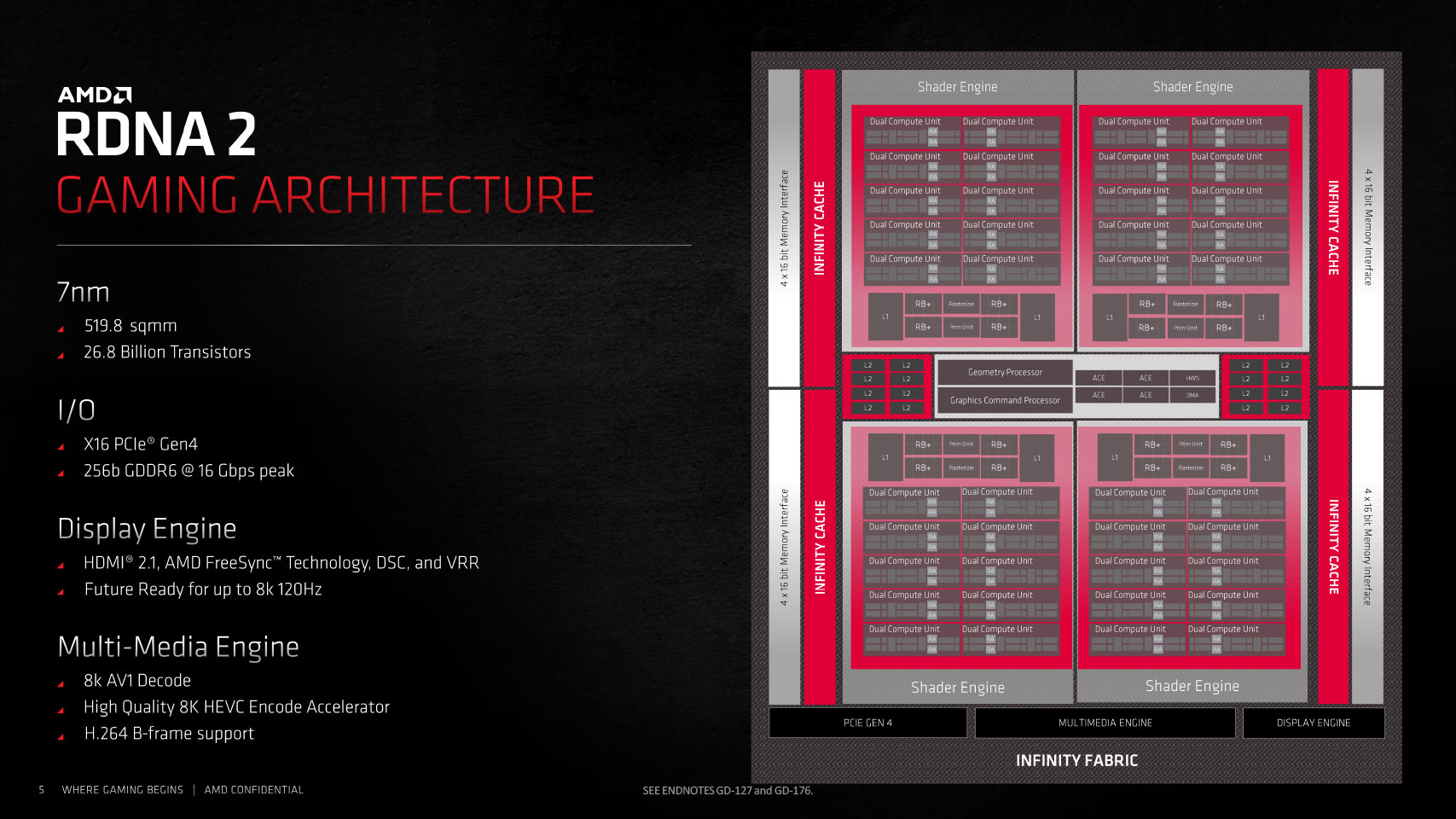
For AMD, a lot is riding on the success of the new RDNA 2 graphics architecture as it powers not just the Radeon RX 6000 series graphics cards, but also the GPU inside next-generation game consoles that are designed for 4K Ultra HD gaming with raytracing—a really tall engineering goal. AMD was first to market with a 7 nm GPU more than 15 months ago, with the original RDNA architecture and "Navi." The company hasn't changed its process node, but implemented a host of new technologies, having acquired experience with the node. At the heart of the Radeon RX 6800 XT and RX 6800 is the 7 nm "Navi 21" silicon, which has been fondly referred to as "Big Navi" over the past year or so. This is a massive 519.8 mm² die with 26.8 billion transistors, which puts it roughly in the same league as NVIDIA's 8 nm "GA102" (28.3 billion transistors on a 628.4 mm² die). The die talks to the outside world with a 256-bit wide GDDR6 memory interface, a PCI-Express 4.0 x16 host interface, and display I/O that's good for multiple 4K or 8K displays due to DSC.

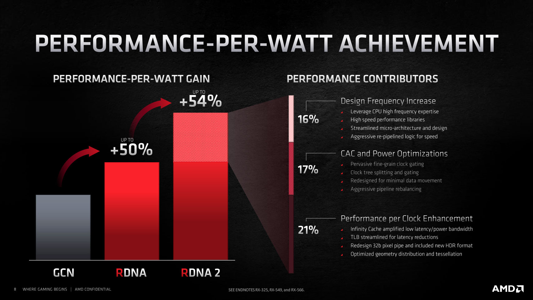
Through new design methodologies and component-level optimization throughout the silicon, along with new power management features, AMD claims to have achieved two breakthroughs that enabled it to double the compute unit counts over the previous generation while staying within a reasonable power envelope. Firstly, the company managed to halve the power draw per CU while adding a 30% increase in engine clocks, which can both be redeemed for performance gain per CU.
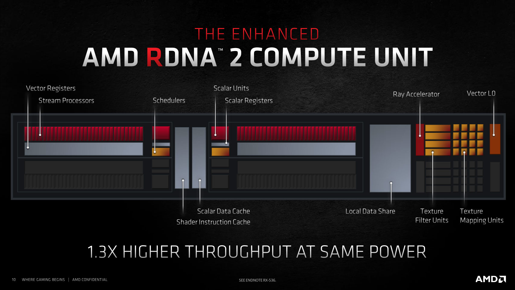

The RDNA 2 compute unit is where a bulk of the magic happens. Arranged in groups of two called Dual Compute Units, which share instruction and data caches, the RDNA 2 compute unit still packs 64 stream processors (128 per Dual CU), and has been optimized for increased frequencies, new kinds of math precision, new hardware that enable the Sampler Feedback feature, and the all-important Ray Accelerator, a fixed-function hardware component that calculates up to one triangle or four box ray intersections per clock cycle. AMD claims the Ray Accelerator makes intersection performance up to ten times faster than if it were to be performed over compute shaders.
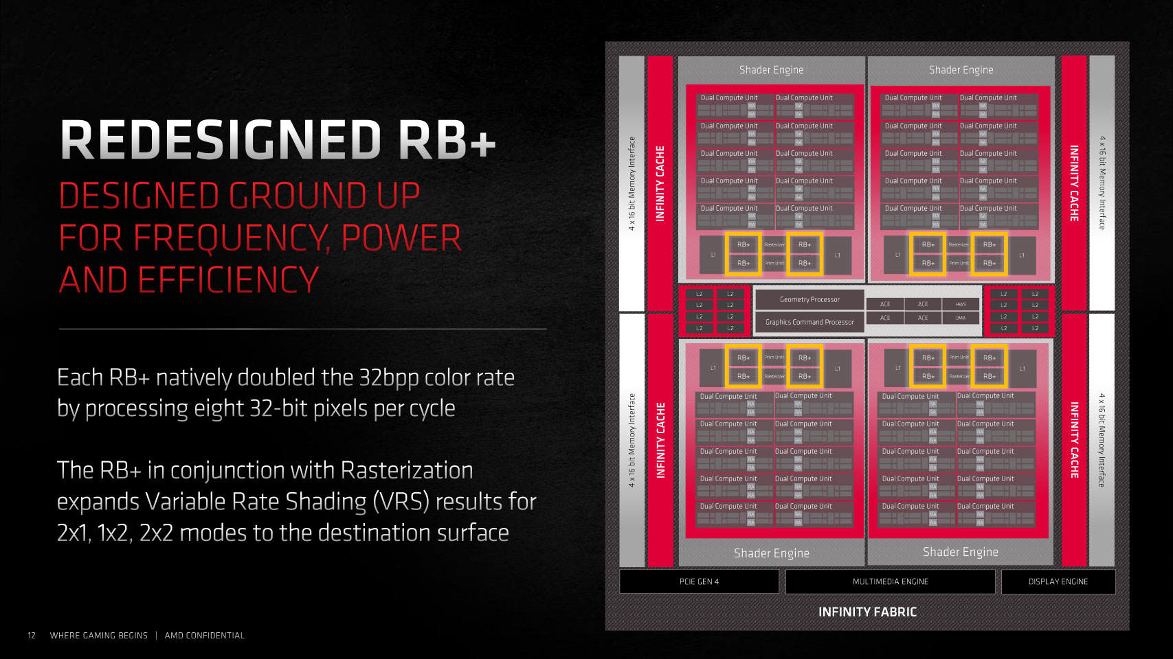
AMD also redesigned the render backends of the GPU from the ground up, towards enabling features such as Variable Rate Shading (both tier-1 and tier-2). The company has doubled ROP counts over "Navi" by giving the chip 128 ROPs. The RX 6800 XT and RX 6900 XT enjoy all 128 ROPs, while the RX 6800 gets 96.
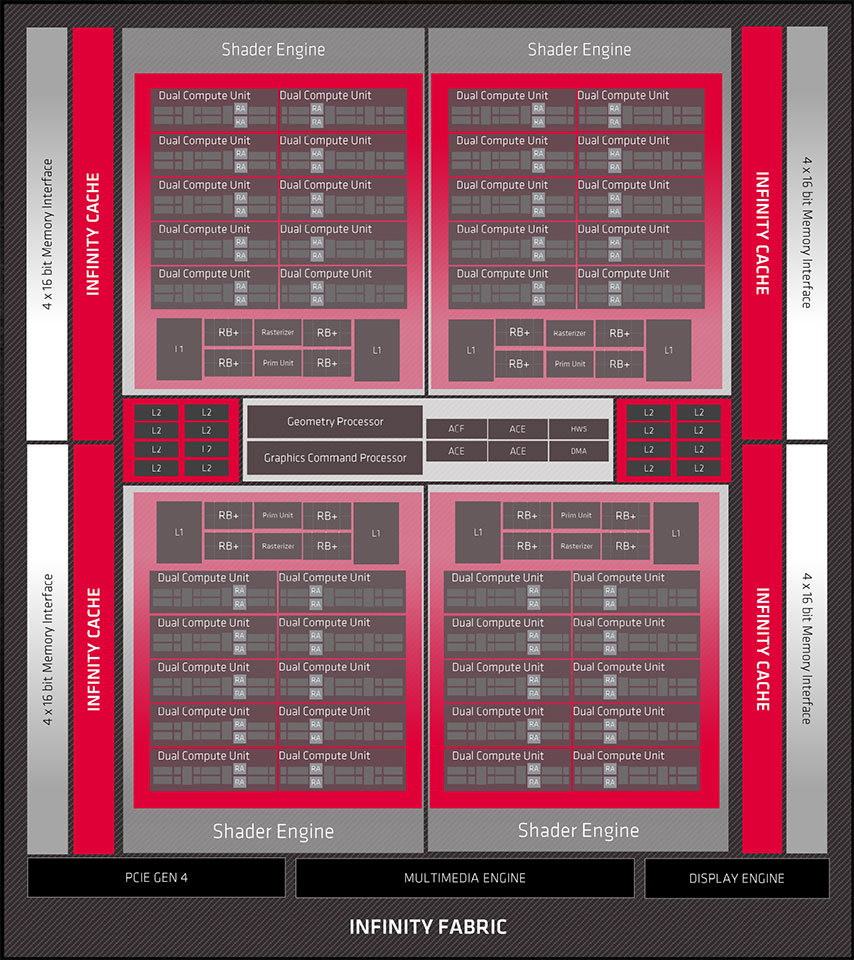
Overall, the "Navi 21" silicon has essentially the same component hierarchy as "Navi 10." The Infinity Fabric interconnect is the link that binds all the components together. At the outermost level, you have the chip's 256-bit GDDR6 memory controllers, a PCI-Express 4.0 x16 host interface, the multimedia- and display engines (which have been substantially updated from RDNA). A notch inside is the chip's 128-megabyte Infinity Cache, which we detail below. This cache is the town-square for the GPU's high-speed 4 MB L2 caches and the Graphics Command Processor, which dispatches the workload among four Shader Engines. Each of these Shader Engines packs 10 RDNA 2 Dual Compute Units (or 20 CUs) along with the updated Render Backends and L1 cache. Combined, the silicon has 5,120 stream processors across 80 CUs, 80 Ray Accelerators (1 per CU), 320 TMUs, and 128 ROPs.
The RX 6800 XT is carved out by enabling 72 out of 80 CUs (one disabled Dual CU per Shader Engine), which works out to 4,608 stream processors, 288 TMUs, and an unchanged 128 ROPs. The RX 6800 is further cut down by enabling 60 out of 80 CUs. It's unclear if a full Shader Engine or 10 random Dual CUs have been disabled to accomplish this. The RX 6800 ends up with 3,840 stream processors, 240 TMUs, 60 Ray Accelerators, and 96 ROPs. The RX 6900 XT, which will be launched in December 2020, maxes out the silicon with all 80 CUs enabled.
Infinity Cache, or How AMD is Blunting NVIDIA's G6X Advantage
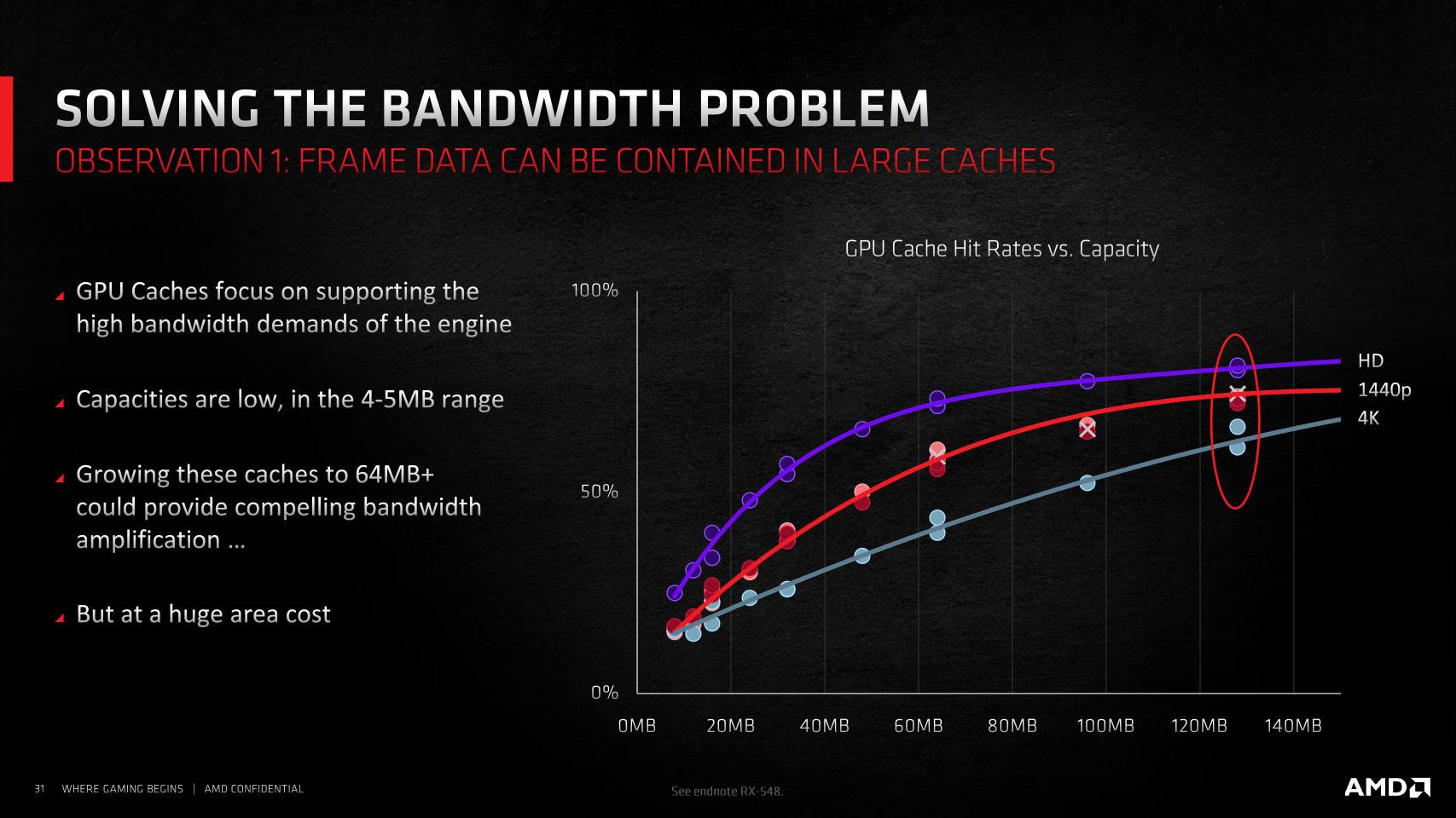
Despite its lofty design goals and a generational doubling in memory size to 16 GB, the RX 6800 XT and RX 6800 have a rather unimpressive memory setup compared to NVIDIA's RTX 3080 and RTX 3090. That is, at least on paper, with just a 256-bit bus width and JEDEC-standard 16 Gbps GDDR6, which works out to 512 GB/s raw bandwidth. NVIDIA has increased bus widths to 320-bit and 384-bit, and innovated 19–19.5 Gbps GDDR6X memory to go with its cards, offering bandwidth rivaling those of 4096-bit HBM2 setups. Memory compression secret-sauce can at best increase effective bandwidth by a high single-digit percent.
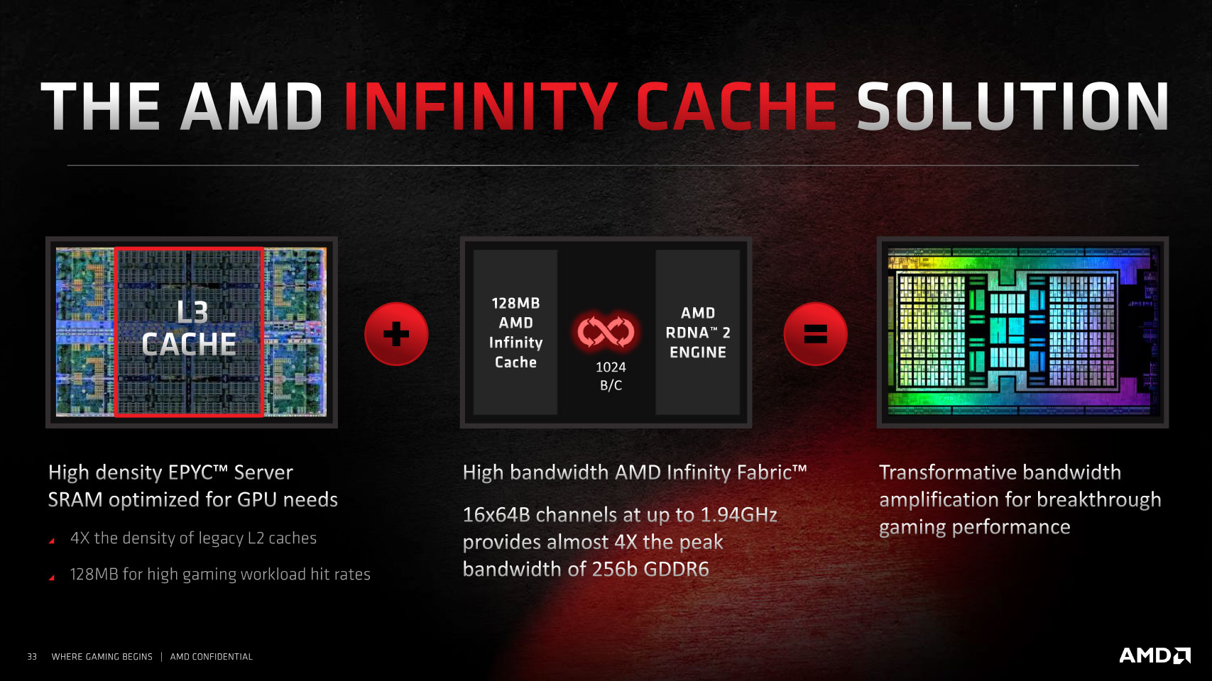

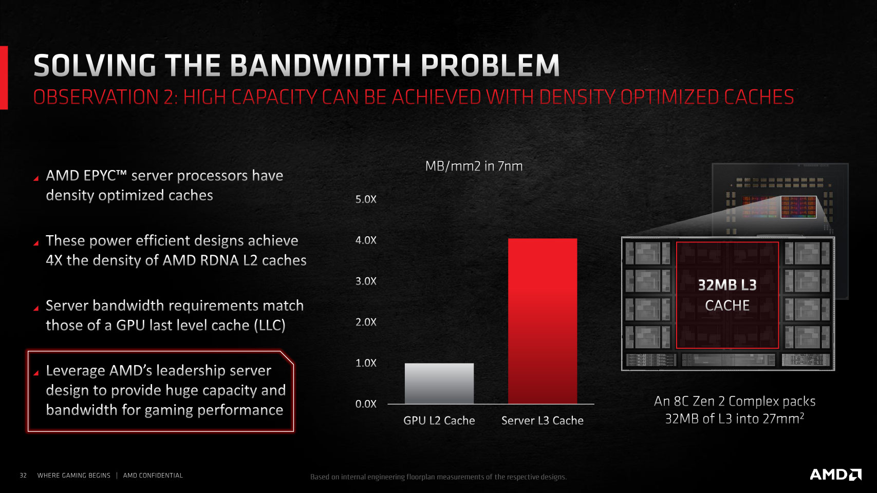
AMD took a frugal approach to this problem, not wanting to invest in expensive HBM+interposer based solutions, which would throw the overall GPU's production costs way off balance. It looked at how AMD's "Zen" processor team leveraged large last-level caches on EPYC processors to significantly improve performance and carried the idea over to the GPU. About 20% the "Navi 21" silicon die area now holds what AMD calls the "Infinite Cache," which is really just a new L3 cache that is 128 MB in size and talks to the GPU's four shader engines at 1024 bits per pin, per cycle. This cache has an impressive bandwidth of 2 TB/s and can be used as a victim cache by the 4 MB L2 caches of the four shader engines.

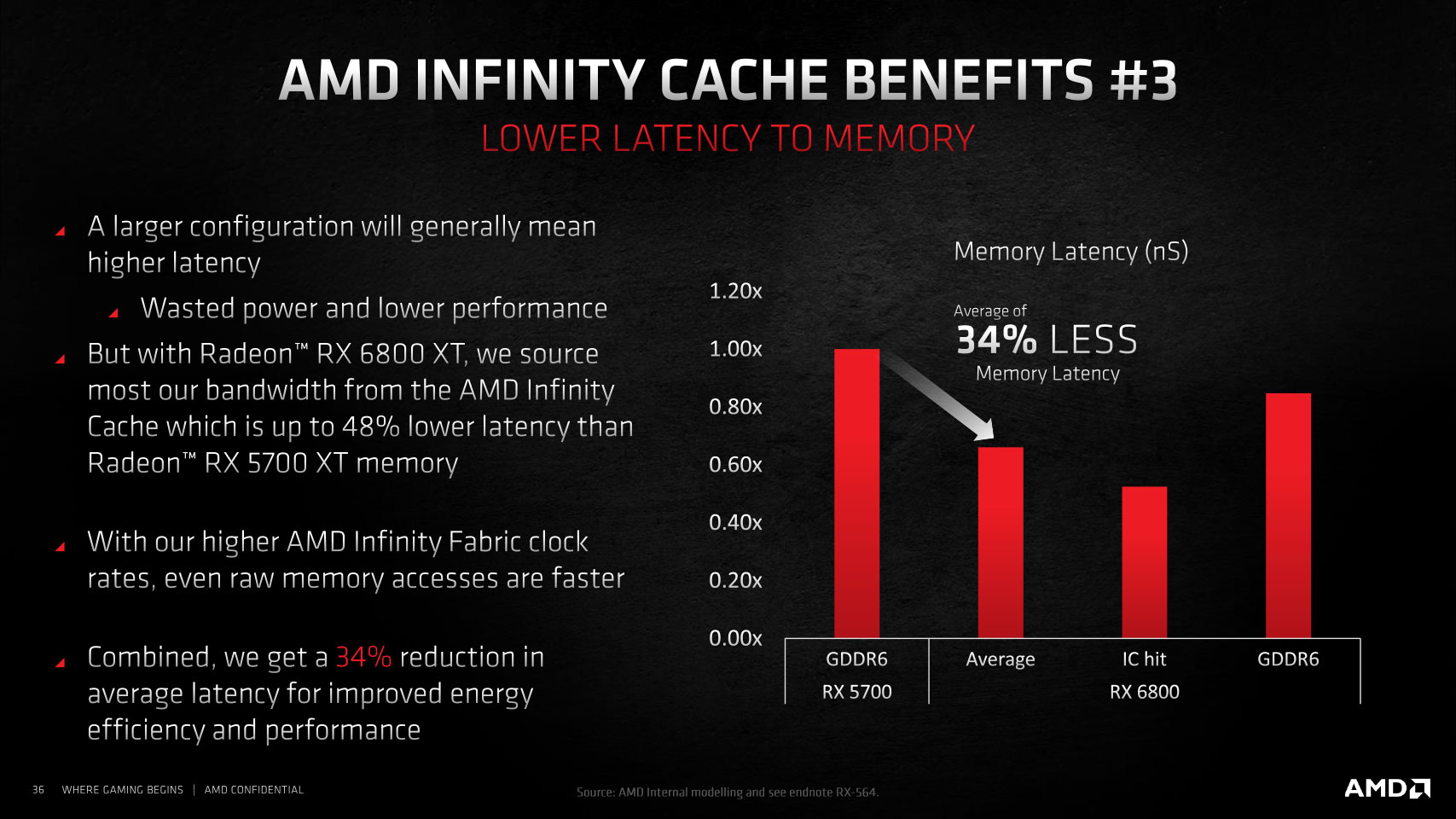
The physical media of Infinity Cache is the same class of SRAM used for the L3 cache on "Zen" processors. It offers four times the density of 4 MB L2 caches, lower bandwidth in comparison, but four times the bandwidth over GDDR6. It also significantly reduces energy consumption, by 1/6th for the GPU to fetch a byte of data compared to doing so from GDDR6 memory. I'm sure the questions on your mind are what difference 128 MB makes and why no one has done this earlier.

To answer the first question, even with just 128 MB spread across two slabs of 64 MB, each, Infinity Cache takes up roughly 20% of the die area of the "Big Navi" silicon, and AMD's data has shown that much of the atomic workloads involved in raytracing and raster operations are bandwidth-intensive rather than memory-size intensive. Having a 128 MB fast victim cache running at extremely low latencies (compared to DRAM) helps. As for why AMD didn't do this earlier, it's only now that there's an alignment of circumstances where the company can afford to go with a fast 128 MB victim cache as opposed to just cramming in more CUs to get comparable levels of performance, but for less power consumption—as a storage device rather than a logic device, spending 20% of the die area on Infinity Cache instead of 16 more CUs does result in power savings.
DirectX 12 Ultimate and Real-Time Raytracing
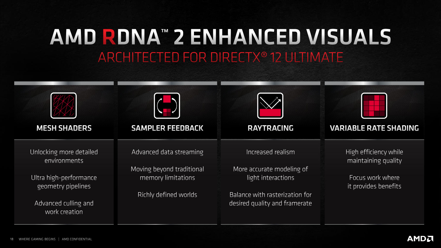
Earlier this year, Microsoft finalized the DirectX 12 Ultimate API subset, which enables improved visual fidelity over conventional DirectX 12. Four features were chosen by Microsoft for GPU vendors to qualify for the new logo—support for real-time raytracing using the DirectX Raytracing or DXR API, Mesh Shaders, Sampler Feedback, and Variable Rate Shading (VRS). AMD worked toward ticking off all four features, and the Xbox Series X/S launched earlier this year became the first DirectX 12 Ultimate device powered by AMD hardware. NVIDIA's "Turing" graphics architecture from 2018 already meets all these requirements.


AMD's implementation of DirectX Raytracing is slightly different from NVIDIA's. The RDNA 2 graphics architecture uses Ray Accelerators, fixed-function hardware which calculate ray intersections with boxes and triangles (4-box intersections per clock, or one triangle intersection per clock). Intersection is the most math-intensive step, which warranted special hardware. Most other stages of the raytracing pipeline leverage the vast SIMD resources at the GPU's disposal, while NVIDIA's RT core offers full BVH traversal processing via special hardware. Also, the two companies take different approaches to de-noising, an important stage of raytracing that seeks to remove the "noise" resulting from the "sparsity" of rays being used. Remember, we're not quite there with fully raytraced 3D scenes, but raster 3D with select raytraced elements is an option. While NVIDIA uses an AI-based de-noiser that leverages tensor cores, AMD's de-noiser leverages compute shaders. The company claims to have innovated an efficient compute-based de-noising solution.


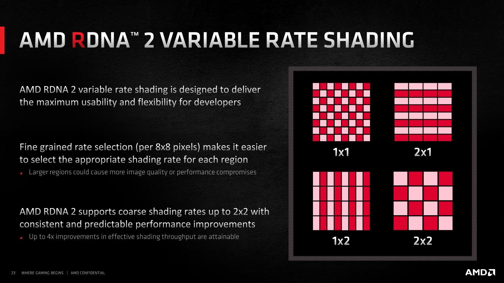
AMD also implemented support for Mesh Shaders as a geometry front end, which again heavily rely on compute shaders, Sampler Feedback, and Variable Rate Shading (VRS), a key feature that allows different regions of a 3D scene to have different levels of shading, letting the GPU conserve resources. RDNA 2 supports both VRS tier-1 and tier-2. VRS, along with dynamic resolution, makes up much of the secret sauce that lets next-gen consoles offer 4K UHD gaming.
Smart Access Memory and DirectStorage
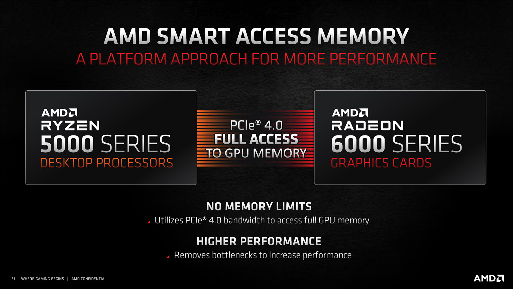
Your CPU can only address up to 256 MB of video memory at once, a legacy from when things were operating in 32-bit mode with 4 GB of address space. Modern graphics cards come with a lot more memory, and in cases where the CPU needs to address more VRAM, a windowing mechanism is used where the GPU keeps a 256 MB chunk of its memory as a transfer area data the CPU requests is juggled in and out of. The 256 MB aperture size was arbitrarily decided on in the 32-bit days when address-space was at a premium. Video cards have plenty of memory bandwidth (compared to main memory totals), so this arrangement didn't really bottleneck anything. AMD is already running a tight ship with its relatively narrow memory bus and Infinity Cache. As such, it sought to change this by using the resizable base address register (BAR) capability standardized by the PCI-SIG, which AMD and NVIDIA hadn't leveraged until now.
AMD simply branded resizable BAR "Smart Access Memory." This feature requires an AMD Ryzen 5000 series processor, an AMD 500-series chipset motherboard, and a UEFI firmware update that toggles the feature, but in theory any modern chipset will support it. With Smart Access Memory, the CPU is able to access the full VRAM as a continuous block of memory. AMD claims that in specific game engines that rely on heavy CPU access of video memory, Smart Access Memory can improve performance by up to six percent. We put these claims to the test in our dedicated AMD Smart Access Memory article.
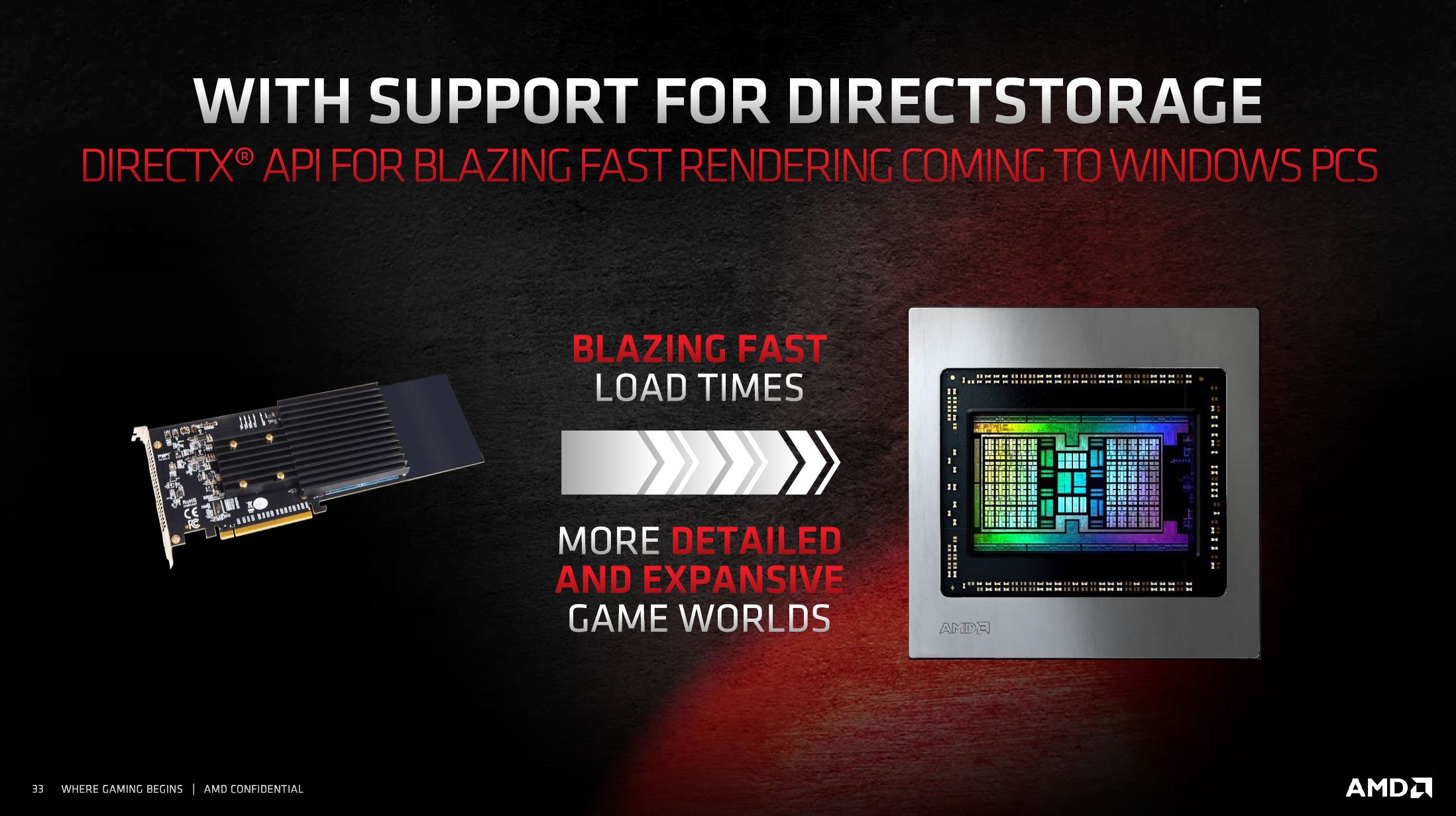
AMD is also introducing support for the DirectStorage API, which can accelerate game-loading times by giving the GPU direct access to game resource data from an NVMe SSD in its native compressed format, and performing the decompression on the GPU, leveraging compute shaders. Since the GPU isn't performing much 3D rendering during level-loading scenes, you won't feel its impact on frame rates, but loading times will be cut down.
Display and Media
AMD substantially updated the display and multimedia engines with RDNA 2. The Radeon RX 6800 series cards come with two DisplayPort 1.4 connectors, one HDMI 2.1 port, and a USB-C port with DisplayPort and USB 3.1 Gen 2, along with up to 27 W USB-PD. Thanks to HDMI 2.1 and Display Stream Compression (DSC), the card now supports 8K at up to 120 Hz resolution, along with support for FreeSync and Variable Refresh Rate. The multimedia engine now has AV1 hardware decode at up to 8K resolution and HEVC hardware encode at up to 8K, along with H.264 B-frame support.
Our Patreon Silver Supporters can read articles in single-page format.
Apr 14th, 2025 02:36 EDT
change timezone
Latest GPU Drivers
New Forum Posts
- 9070XT or 7900XT or 7900XTX (190)
- What's your latest tech purchase? (23542)
- RX 9000 series GPU Owners Club (313)
- Multiple major problems that i can't explain (1)
- Game Soundtracks You Love (1038)
- Advice on GPU upgrade (19)
- Anime Nation (13022)
- ThrottleStop - 14900HX, 4090RTX MSI laptop (13)
- TPU's Nostalgic Hardware Club (20237)
- Need some help with vbios flashing (1)
Popular Reviews
- TerraMaster F8 SSD Plus Review - Compact and quiet
- ASUS GeForce RTX 5080 TUF OC Review
- Thermaltake TR100 Review
- The Last Of Us Part 2 Performance Benchmark Review - 30 GPUs Compared
- Zotac GeForce RTX 5070 Ti Amp Extreme Review
- Sapphire Radeon RX 9070 XT Pulse Review
- Sapphire Radeon RX 9070 XT Nitro+ Review - Beating NVIDIA
- Upcoming Hardware Launches 2025 (Updated Apr 2025)
- MSI MAG CORELIQUID A15 360 Review
- ASRock Z890 Taichi OCF Review
Controversial News Posts
- NVIDIA GeForce RTX 5060 Ti 16 GB SKU Likely Launching at $499, According to Supply Chain Leak (181)
- MSI Doesn't Plan Radeon RX 9000 Series GPUs, Skips AMD RDNA 4 Generation Entirely (146)
- NVIDIA Sends MSRP Numbers to Partners: GeForce RTX 5060 Ti 8 GB at $379, RTX 5060 Ti 16 GB at $429 (124)
- Microsoft Introduces Copilot for Gaming (124)
- Nintendo Confirms That Switch 2 Joy-Cons Will Not Utilize Hall Effect Stick Technology (105)
- Over 200,000 Sold Radeon RX 9070 and RX 9070 XT GPUs? AMD Says No Number was Given (100)
- Nintendo Switch 2 Launches June 5 at $449.99 with New Hardware and Games (99)
- NVIDIA PhysX and Flow Made Fully Open-Source (77)