 135
135
AMD Radeon RX 7900 XT Review
(135 Comments) »Introduction
The new RDNA 3 graphics architecture releases today, and leading from the top are the new Radeon RX 7900 XT (in this review), and the RX 7900 XTX flagship, which we've also reviewed today. Both these graphics cards are designed to take the fight to NVIDIA's high-end: the GeForce RTX 40-series "Ada," but at highly competitive prices. The RX 7900 XT from this review targets a slightly lower price-point than the RX 7900 XTX flagship, while being designed for the exact same class of gaming—4K Ultra HD maxed out with ray tracing. The new RDNA 3 architecture promises to repeat the 50% leap in performance/Watt that made it possible for AMD to return to the high-end graphics segment with their RX 6000 series RDNA 2.

The company still believes that Moore's Law exists, and that it requires efficiently utilizing the various foundry nodes to optimize cost. This is basically what AMD does in the CPU space, something it debuted with the Ryzen 3000 series and 2nd Gen EPYC processors. The CPU cores are built on the latest node, while the memory controller isn't. In the same way, the stream processors and other number crunching machinery of the Shader Engines are built on a centralized Graphics Compute Die (GCD) that's fabricated on the latest 5 nm EUV foundry node; while the Infinity Cache memory, memory controllers, and GDDR6 PHY, are pushed to multiple Memory Cache Dies (MCDs), built on the slightly older 6 nm node. The "Navi 31" silicon on which the RX 7900 series is based, features six of these, and hence has a 384-bit wide memory interface. Five of these are enabled on the RX 7900 XT, hence it ends up with a 320-bit memory interface. Each MCD has a 16 MB piece of the GPU's 96 MB Infinity Cache, the RX 7900 XT gets 80 MB of it.
AMD carved the Radeon RX 7900 XT in this review from the "Navi 31" GPU, by enabling 84 out of 96 RDNA 3 compute units physically present on the silicon, and 5 out of 6 MCDs. This results in hardware specs of 5,376 (out of 6,144) stream processors, 336 (out of 384) TMUs, the chip's full 192 ROP count, and a 320-bit GDDR6 memory interface, which runs 20 GB of 20 Gbps memory, resulting in an impressive 800 GB/s memory bandwidth.
The RDNA 3 graphics architecture introduced dual issue-rate compute units, with a high degree of optimization in the way idle SIMD resources are utilized, support for newer math formats, and a new AI accelerator that retasks the SIMD resources for matrix math functions. Together, these optimizations produce a 17% IPC uplift over the RDNA 2 CU. There are 96 CUs on the silicon, which work out to 6,144 stream processors. The architecture also sees an increase in engine clocks, and a decoupling of the shader clock speeds to those of the GPU's Front End, which operates at a 10-15% higher frequency. The most striking aspect of the RDNA 3 architecture is that the typical board power of these GPUs is well contained, with the RX 7900 XTX rated at just 350 W, and the RX 7900 XT at 315 W—both of which can be fed by just two 8-pin PCIe power connectors, and cooled by solutions much smaller than those found on the competing NVIDIA GeForce RTX 4080 or RTX 4090 "Ada."
AMD is transferring the costs saved with its chiplet architecture over to customers, by aggressively pricing the Radeon RX 7900 XT at $900. Its bigger sibling, the RX 7900 XTX, goes for just $1,000. Compared to these, the NVIDIA offerings are quite expensive, with the RTX 4080 priced at $1,200 and the flagship RTX 4090 at $1,600. What's more, the RX 7900 XT has a typical power of just 315 W, and makes do with two conventional 8-pin PCIe power connectors, and the reference board design by AMD is as compact as the RTX 3080 Founders Edition, making it friendly with even some SFF cases. In this review, we compare the RX 7900 XT with its segment rivals, as well as a small but growing selection of graphics cards, on our swanky new 13900K-based VGA test-bench.
| Price | Cores | ROPs | Core Clock | Boost Clock | Memory Clock | GPU | Transistors | Memory | |
|---|---|---|---|---|---|---|---|---|---|
| RTX 3070 | $500 | 5888 | 96 | 1500 MHz | 1725 MHz | 1750 MHz | GA104 | 17400M | 8 GB, GDDR6, 256-bit |
| RTX 3070 Ti | $600 | 6144 | 96 | 1575 MHz | 1770 MHz | 1188 MHz | GA104 | 17400M | 8 GB, GDDR6X, 256-bit |
| RX 6800 | $510 | 3840 | 96 | 1815 MHz | 2105 MHz | 2000 MHz | Navi 21 | 26800M | 16 GB, GDDR6, 256-bit |
| RX 6800 XT | $650 | 4608 | 128 | 2015 MHz | 2250 MHz | 2000 MHz | Navi 21 | 26800M | 16 GB, GDDR6, 256-bit |
| RTX 3080 | $750 | 8704 | 96 | 1440 MHz | 1710 MHz | 1188 MHz | GA102 | 28000M | 10 GB, GDDR6X, 320-bit |
| RTX 3080 Ti | $950 | 10240 | 112 | 1365 MHz | 1665 MHz | 1188 MHz | GA102 | 28000M | 12 GB, GDDR6X, 384-bit |
| RX 6900 XT | $700 | 5120 | 128 | 2015 MHz | 2250 MHz | 2000 MHz | Navi 21 | 26800M | 16 GB, GDDR6, 256-bit |
| RX 6950 XT | $800 | 5120 | 128 | 2100 MHz | 2310 MHz | 2250 MHz | Navi 21 | 26800M | 16 GB, GDDR6, 256-bit |
| RTX 3090 | $950 | 10496 | 112 | 1395 MHz | 1695 MHz | 1219 MHz | GA102 | 28000M | 24 GB, GDDR6X, 384-bit |
| RX 7900 XT | $900 | 5376 | 192 | 2000 MHz | 2400 MHz | 2500 MHz | Navi 31 | 57700M | 20 GB, GDDR6, 320-bit |
| RTX 3090 Ti | $1400 | 10752 | 112 | 1560 MHz | 1950 MHz | 1313 MHz | GA102 | 28000M | 24 GB, GDDR6X, 384-bit |
| RTX 4080 | $1200 | 9728 | 112 | 2205 MHz | 2505 MHz | 1400 MHz | AD103 | 45900M | 16 GB, GDDR6X, 256-bit |
| RX 7900 XTX | $1000 | 6144 | 192 | 2300 MHz | 2500 MHz | 2500 MHz | Navi 31 | 57700M | 24 GB, GDDR6, 384-bit |
| RTX 4090 | $2400 | 16384 | 176 | 2235 MHz | 2520 MHz | 1313 MHz | AD102 | 76300M | 24 GB, GDDR6X, 384-bit |
AMD RDNA 3 Graphics Architecture


The Radeon RX 7900 XTX and RX 7900 XT debut AMD's 3rd generation RDNA graphics architecture, termed RDNA 3. With it, AMD plans to repeat the generational 50% performance/Watt gain it achieved with RDNA 2, which sprung it back to the high-end graphics segment after a long gap. AMD claims it succeeded in this endeavor, with a 54% generational performance/Watt gain. At the heart of this effort is the switch to the new TSMC 5 nm EUV foundry node. AMD figured out early on that it cannot build large monolithic GPUs on 5 nm without thinning its margins in the fight against NVIDIA, and set out to innovate the Chiplet architecture for the GPU. Under this, specific parts of the GPU that actually benefit from a switch to a newer foundry node, such as the Shader Engines, would be built on a centralized 5 nm die called the Graphics Compute Die (GCD), while those components that can make do with a less advanced node, namely the memory controllers and L3 cache, would be spun off to chiplets called Memory Cache Dies (MCDs), built on 6 nm.


The "Navi 31" GPU is hence a chiplet GPU and not a multi-chip module like "Vega 10." In a chiplet-based device, various components that can otherwise not exist on their own packages, are placed on a single package, with the goal of minimizing production costs, by stratifying their need for a new foundry node, such that only the most power-intensive IP receive the most advanced node. In a MCM, chips that can otherwise exist on their own package, are combined onto a single package for conserving PCB real-estate, or reducing latency. The GCD in the "Navi 31" GPU hence has all the shader engines, caches up to L2, the front-end Command Processor, Async Compute Engines (ACEs), the Display Engine, and the Media Engine. Each of the six MCDs has a 64-bit wide memory bus, and a 16 MB segment of the GPU's 96 MB Infinity Cache memory. The size of the Infinity Cache may have been generationally reduced (compared to 128 MB on "Navi 21"), but AMD has widened the memory bus itself, from 256-bit up to 384-bit.
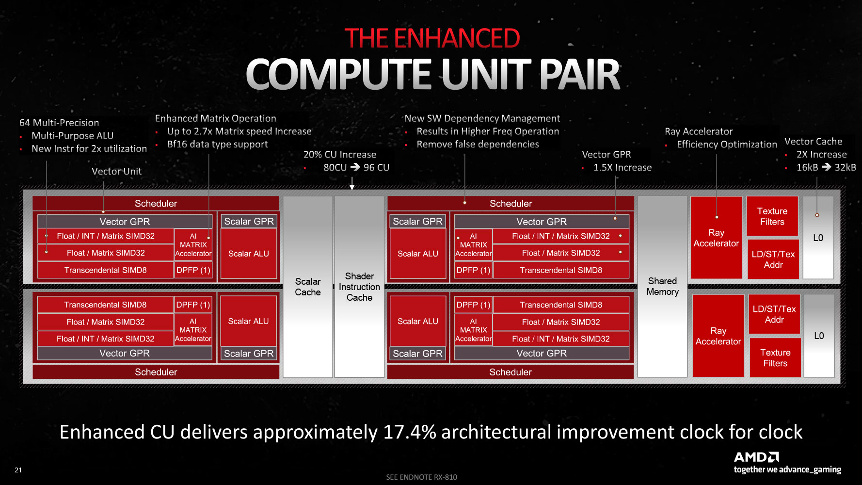

Much of the architectural innovation is not with the chiplet design (a packaging innovation); but at the level of the RDNA 3 Dual-Compute Unit (or Compute Unit pair). The "Navi 31" GPU physically features 96 compute units spread across six Shader Engines. AMD claims that at the same engine clocks, the RDNA 3 CU offers a 17.4% IPC increase over the RDNA 2 CU. There are 20% more CUs over the "Navi 21," and these run at higher engine clocks, tapping into the power headroom afforded by the 5 nm process. These combined work out to the 54% generational performance uplift, with which AMD plans to retain competitiveness with NVIDIA's RTX 40-series "Ada" high-end SKUs.


The new RDNA 3 CU introduces multi-precision capability for the 64 stream processors per CU: operating either as 1x SIMD64 or 2x SIMD32 units. The Vector Unit that houses these SIMD units can either function as a SIMD execution mechanism, or as a Matrix execution unit, thanks to the new AI Matrix Accelerator, which provides a 2.7x matrix multiplication performance uplift versus conventional SIMD execution. Also added are support for the Bfloat16 instruction-set, and SIMD8 execution. The GPU hence enjoys AI hardware-acceleration that can be leveraged in future feature-additions relevant to gamers, such as FSR 3.0. Game developers will also look for ways to exploit accelerated AI, now that all three brands feature it (NVIDIA Tensor cores and Intel XMX cores).


AMD's first-generation Ray Accelerator, introduced with the RDNA 2 architecture, was the result of a hasty effort to catch up to NVIDIA with a DirectX 12 Ultimate GPU, where they developed a fixed-function hardware to calculate ray intersections, and offloaded a large chunk of RT processing to the generationally-doubled SIMD resources. With RDNA 3, they've refined the Ray Accelerator to achieve an 80% ray tracing performance uplift over the previous generation, when you add up the Ray Accelerator count, their higher engine clocks, and other hardware-level optimizations, such as early sub-tree culling, specialized box sorting modes, and reduced traversal iterations.

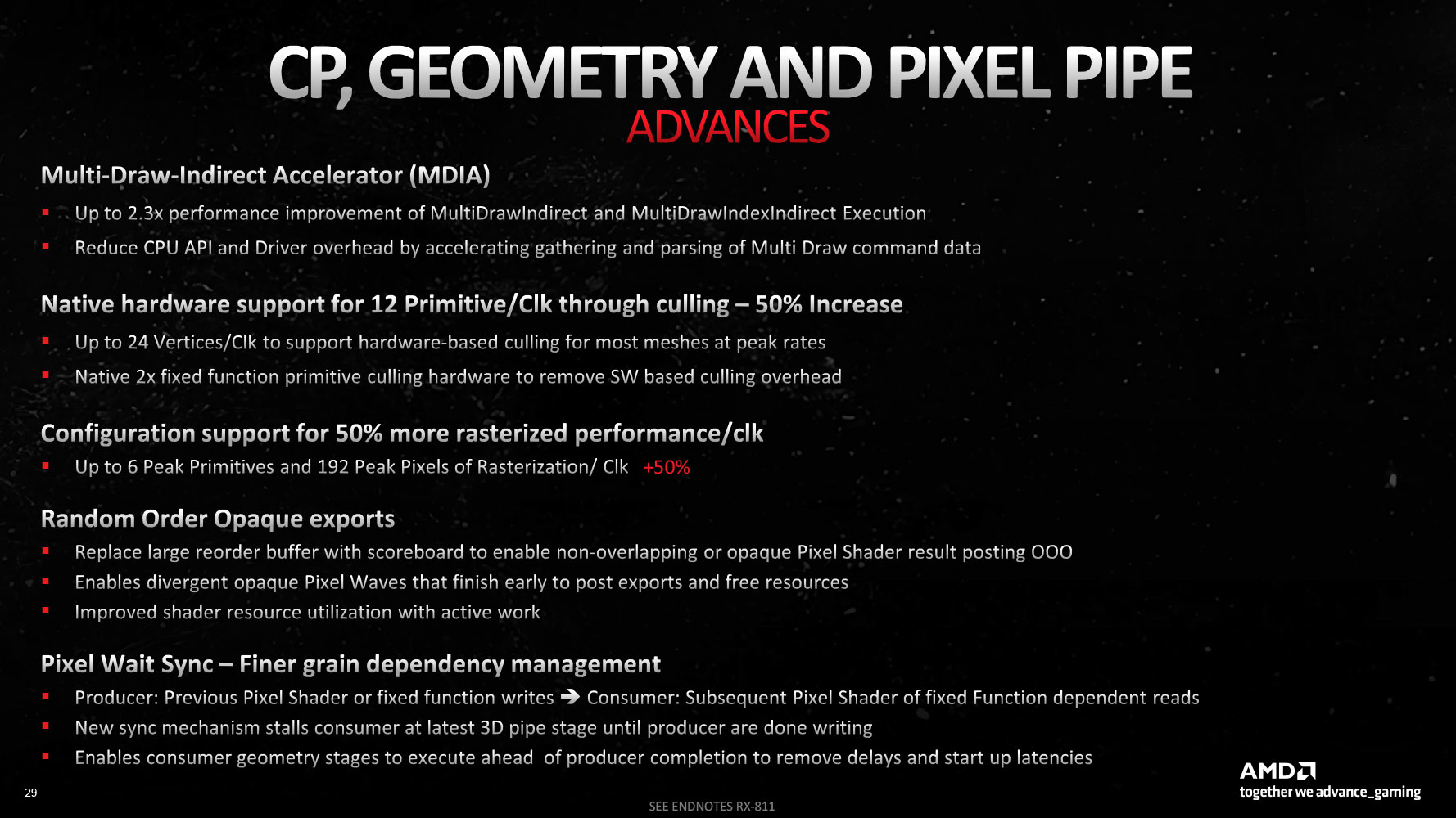
There is a 50% ray intersection capacity improvement for the "Navi 31" GPU thanks to these optimizations, and cycles-per-ray reduction. Besides these, AMD has also made several improvements to the geometry- and pixel-pipes, with the introduction of the new multi-draw indirect accelerator (MDIA), which reduces CPU API and driver-level overheads by gathering and parsing of multi-draw command data. At the hardware-level 12 primitives per clock is now supported compared to 8 per clock on RDNA 2, thanks to culling. The core-configuration overall enables 50% more rasterized performance per clock.
The GCD features six Shader Engines, each with 16 compute units (or 8 dual compute units), which work out to 1,024 stream processors. Six such Shader Engines make up 6,144 stream processors with 96 Ray Accelerators and 96 AI Accelerators. The GPU has 384 TMUs, and a massive 192 ROPs—a 50% increase over "Navi 21." The Radeon RX 7900 XTX enables all 96 CUs, and maxes out the silicon, whereas the RX 7900 XT has 84 out of 96 CUs enabled, which work out to 5,376 stream processors, 84 Ray Accelerators, 336 TMUs, and an unchanged 192 ROPs. The RX 7900 XTX gets 24 GB of GDDR6 memory across the GPU's entire 384-bit memory bus, with a memory speed of 20 Gbps (GDDR6-effective), which means 960 GB/s of memory bandwidth. The RX 7900 XT is equipped with 20 GB of memory across a narrower 320-bit memory bus carved out by disabling one of the six MCDs. At the same 20 Gbps speed, this yields 800 GB/s bandwidth.


AMD has significantly improved the Display Engine of "Navi 31" over the previous-generation in terms of connectivity. The new Radiance Display Engine comes with native support for DisplayPort 2.1, which enables 8K output at up to 165 Hz refresh-rate, or 4K at up to 480 Hz, with a single cable. AMD has refined its FSR 2 algorithm to support 8K (i.e. render at a lower resolution with FSR-enhanced upscaling), to make it possible to enjoy the latest AAA titles at playable frame-rates on 8K displays. Both the RX 7900 series cards get two full-size DP 2.1 connectors, besides an HDMI 2.1b, and a USB-C with DP 1.2 passthrough. The "Navi 31" silicon receives full hardware-accelerated AV1 encode and decode capabilities, through dual independent encode/decoders, so two independent video streams can be simultaneously transcoded, or one stream at twice the framerate. With this generation, AMD is also introducing SmartAccess Video, a feature that lets the AMD driver leverage the hardware encoders of the RDNA 2 iGPU of Ryzen 7000 desktop processors, for additional encoding performance.
Packaging


The Card


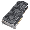
The AMD Radeon RX 7900 XT follows the same design theme as the XTX, it looks fantastic, but is just a little bit smaller. AMD has refined their design approach even further, the card is dominated by black in various shades of gray. On the metal backplate you get some red highlights, and three fins on the side have been painted red to represent the third generation of the RDNA architecture.

The Radeon RX 7900 XT has no RGB lighting, the gray/white highlights on the front cooler are fixed-color plastic.


Dimensions of the card are 28.0 x 11.5 cm, and it weighs 1533 g.
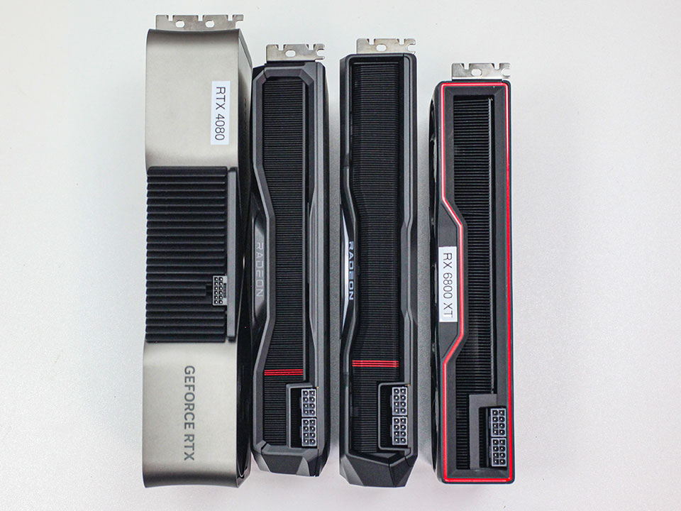


Here's various comparisons to other relevant cards. The RX 7900 Series is clearly much more compact than the offerings from NVIDIA.


The Radeon RX 7900 XT is slightly smaller than the XTX.


Installation requires three slots in your system.

Display connectivity includes two standard DisplayPort 2.1 ports (RDNA 2 had 1.4a) and one HDMI 2.1a (same as RDNA 2). The USB-C port that you see is not a classic USB port that you can attach storage to, it only supports DisplayPort 2.1 passthrough + PD, for use with VR.
AMD has upgraded their encode/decode setup. It now comes with two independent hardware units that can encode and decode two streams of video in parallel, or one stream at double the FPS rate. There's support for VP9, H.264, H.265 and AV1 decode, and encoding is supported for H.264, H.265 and AV1.

The card uses a classic dual 8-pin power input config, rated for 375 W of maximum power. NVIDIA on the other hand uses the new 12+4 pin ATX 12VHPWR connector, rated for up to 600 W of power draw. This makes it easy to install the AMD card in older systems, but it does limit their maximum current delivery capability. Some custom board designs of the RX 7900 XTX will have three power inputs.
Teardown
Taking the RX 7900 XT apart is really easy, it's straightforward to disassemble and maintain.

The main heatsink provides cooling for the GPU chip, memory chips and VRM circuitry.


After removing the fan assembly, we can see that AMD is using a very large vapor-chamber that has fins directly attached to it. There's no heatpipes in use.


The backplate is made from thick metal and of excellent build quality. It protects the card against damage during installation and handling.
High-resolution PCB Pictures
These pictures are for the convenience of volt modders and people who would like to see all the finer details on the PCB. Feel free to link back to us and use these in your articles, videos or forum posts.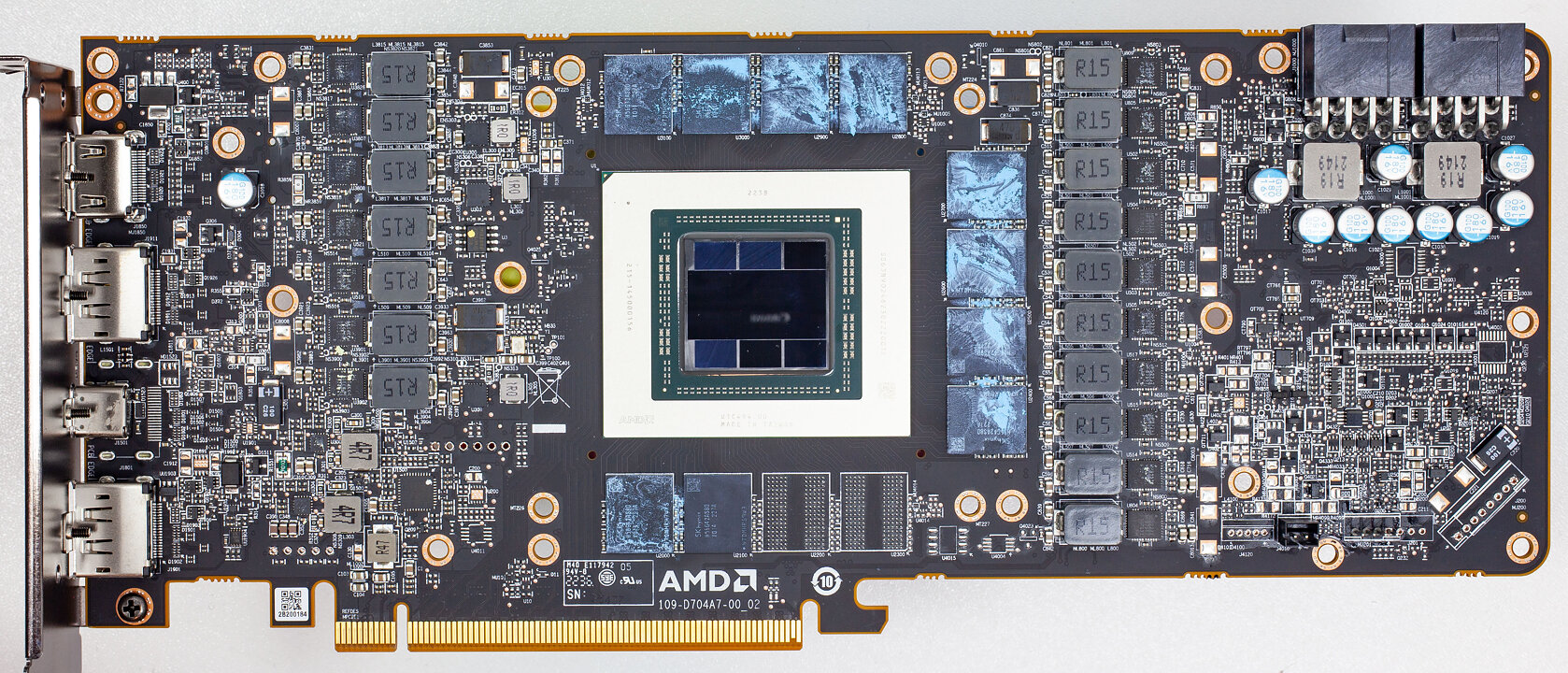
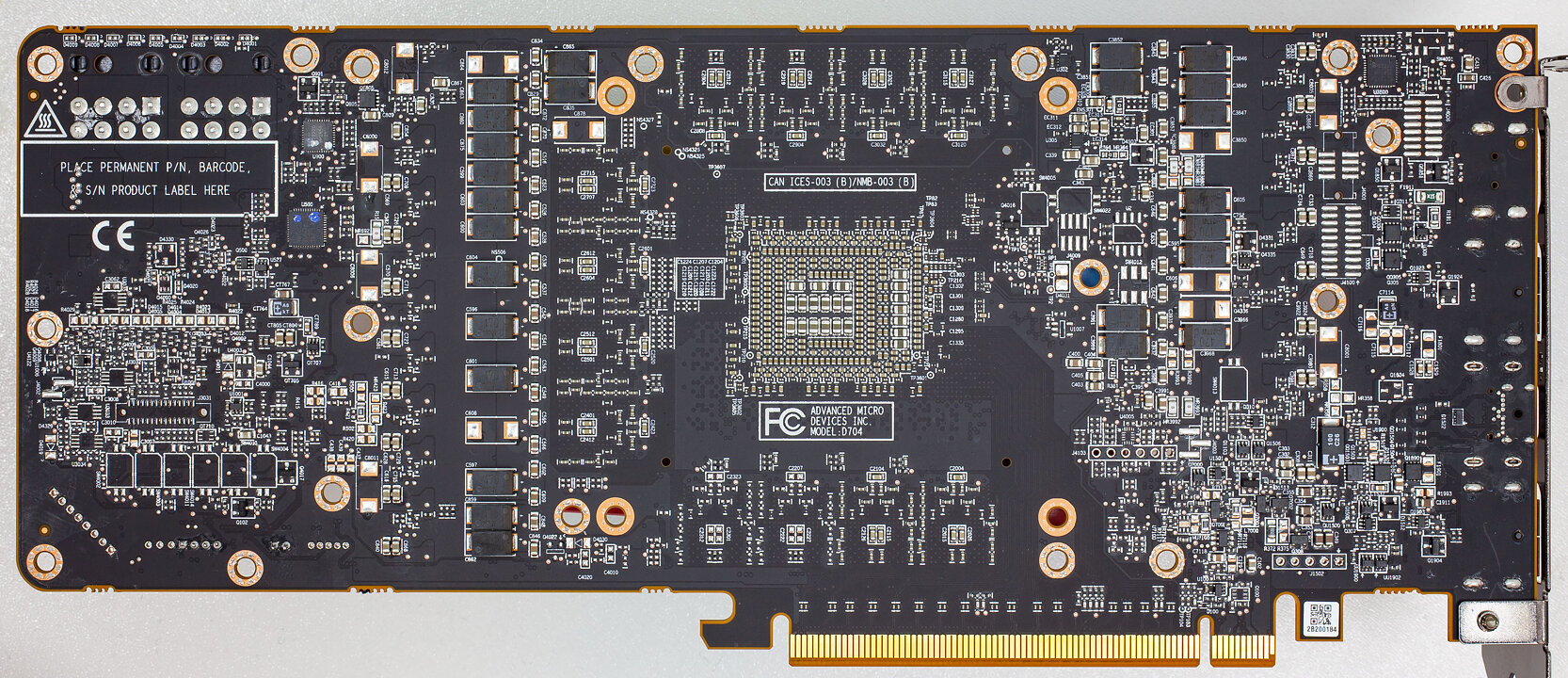
High-resolution versions are also available (front, back).
Our Patreon Silver Supporters can read articles in single-page format.
May 6th, 2025 05:11 EDT
change timezone
Latest GPU Drivers
New Forum Posts
- Choosing an Internal HDD (64)
- Vertical mice in gaming (26)
- Half Life 3 soon ? (20)
- The TPU UK Clubhouse (26204)
- Windows 11 General Discussion (6030)
- What's your latest tech purchase? (23723)
- Dear AMD, NVIDIA, INTEL and others, we need cheap (192-bit to 384-bit), high VRAM, consumer, GPUs to locally self-host/inference AI/LLMs (107)
- TechPowerUP Wallpapers ! (915)
- I dont understand the phone OS world..... (205)
- It's happening again, melting 12v high pwr connectors (1073)
Popular Reviews
- Arctic Liquid Freezer III Pro 360 A-RGB Review
- ASUS Radeon RX 9070 XT TUF OC Review
- Clair Obscur: Expedition 33 Performance Benchmark Review - 33 GPUs Tested
- ASUS ROG Maximus Z890 Hero Review
- Zotac GeForce RTX 5070 Ti Amp Extreme Review
- Upcoming Hardware Launches 2025 (Updated Apr 2025)
- Seasonic Vertex GX 850 W Review
- Sapphire Radeon RX 9070 XT Nitro+ Review - Beating NVIDIA
- ASUS GeForce RTX 5090 Astral Liquid OC Review - The Most Expensive GPU I've Ever Tested
- Montech HS02 PRO Review
Controversial News Posts
- AMD Radeon RX 9060 XT to Roll Out 8 GB GDDR6 Edition, Despite Rumors (131)
- NVIDIA Sends MSRP Numbers to Partners: GeForce RTX 5060 Ti 8 GB at $379, RTX 5060 Ti 16 GB at $429 (128)
- NVIDIA Launches GeForce RTX 5060 Series, Beginning with RTX 5060 Ti This Week (115)
- Nintendo Confirms That Switch 2 Joy-Cons Will Not Utilize Hall Effect Stick Technology (105)
- Sony Increases the PS5 Pricing in EMEA and ANZ by Around 25 Percent (84)
- Parts of NVIDIA GeForce RTX 50 Series GPU PCB Reach Over 100°C: Report (78)
- Intel "Bartlett Lake-S" Gaming CPU is Possible, More Hints Appear for a 12 P-Core SKU (77)
- China Develops HDMI Alternative: 192 Gbps Speeds and 480 W Power Delivery (74)