 553
553
AMD Radeon VII 16 GB Review
Packaging & Contents »2nd Generation Vega Architecture


It may appear like the underlying architecture of Radeon VII is exactly the same as the RX Vega 64 from 2017, codenamed "Vega," but that's not entirely true. Radeon VII is based on what AMD refers to as "Enhanced 2nd Generation Vega architecture."
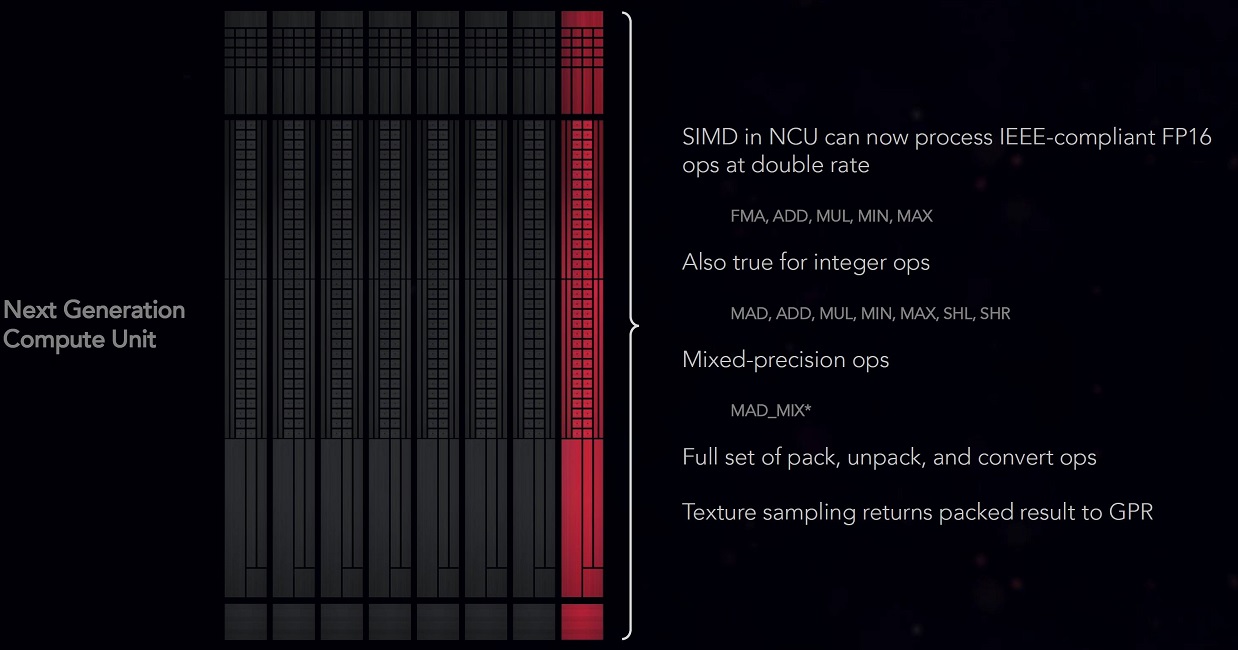
What's new are optimizations that increase frequency by tapping into the engine clock headroom dividend from the switch to 7 nm, reduced latencies across the silicon (think caches, memory controllers, buffers, etc.), increased bandwidth to the 64 ROPs, and notable changes to the "Vega" NGCU (next generation compute unit) that include additional integer and floating-point accumulators, which probably increases IPC a few percentage points.
AMD has also doubled down on the chip's power-management features, beginning with something it calls "Enhanced Thermal Monitoring." The company has sprinkled double the number of temperature sensors across the GPU die. Clock-speed control is now based on junction temperature, which represents data from a larger network of sensors that lets the GPU more accurately control its frequency and voltages, which translates to better sustainability of boost frequencies. This also means the GPU can throttle itself more accurately to maintain reliability of the silicon. AMD presented its own tests that show throttling based on junction temperature rather than edge temperature results in a two percent performance uplift due to better boost frequency sustainability.
The most obvious improvement, though, is the memory interface, which is 4096-bit wide, twice that of "Vega 10," which doubles the memory bandwidth. AMD also chose to equip the Radeon VII with 16 GB of HBM2 memory, doubling it from the previous generation.

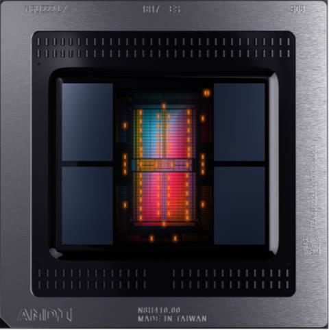
Much like the "Vega 10" that powers the RX Vega 64, the "Vega 20" GPU at the heart of the Radeon VII is a multi-chip module (MCM), a combination of the 7 nm GPU die, four 10 nm-class HBM2 memory stacks supplied by either SK Hynix or Samsung, and a silicon interposer on which the GPU and HBM2 stacks sit. The interposer enables high-density microscopic wiring between the GPU and memory stacks, while TSVs (through silicon vias) connect the GPU and memory stacks to the fiberglass package substrate underneath. The switch to 7 nm has reduced the die-size of the GPU from 495 mm² on the 14 nm "Vega 10" down to 331 mm², which isn't half, but one should realize that "Vega 20" isn't an optical-shrink as there are numerous physical changes to the die which we described above.
Barring small changes to the NGCUs, as lower-latency caches and additional accumulators for both the integer and floating-point sides, the number-crunching resources of "Vega 20" and the chip's hierarchy is essentially the same. The GPU physically features 64 NGCUs, although only 60 of them are enabled on the Radeon VII. This is probably done to increase yields/harvesting of the silicon. These 60 NGCUs amount to 3,840 stream processors and 240 TMUs. The ROP count is unchanged at 64, although AMD has increased the bandwidth of these ROPs. The memory bus width has doubled to 4096-bit, as has the memory amount at 16 GB.
Apr 22nd, 2025 22:52 CDT
change timezone
Latest GPU Drivers
New Forum Posts
- Pls help me decide on a stop-gap upgrade (CAD currency) (31)
- Which is the best replacement for Microsoft Office? (1)
- Deal or no Deal Threadripper WX? (41)
- How to move partitions for free? (W11) (4)
- I dont understand the phone OS world..... (16)
- Are the 8 GB cards worth it? (31)
- How do I get rid of the extra vertical space Linux Ubuntu forces on me? i want more vertical space while browsing the web (1)
- To distill or not distill what say ye? (57)
- am i alone to still using an asus p6t motherboard in the world ? (98)
- RTX5000 Series Owners Club (189)
Popular Reviews
- ASRock X870E Taichi Lite Review
- ASUS GeForce RTX 5060 Ti TUF OC 16 GB Review
- NVIDIA GeForce RTX 5060 Ti 8 GB Review - So Many Compromises
- NVIDIA GeForce RTX 5060 Ti PCI-Express x8 Scaling
- Upcoming Hardware Launches 2025 (Updated Apr 2025)
- Sapphire Radeon RX 9070 XT Pulse Review
- Sapphire Radeon RX 9070 XT Nitro+ Review - Beating NVIDIA
- Palit GeForce RTX 5060 Ti Infinity 3 16 GB Review
- MSI GeForce RTX 5060 Ti Gaming OC 16 GB Review
- AMD Ryzen 7 9800X3D Review - The Best Gaming Processor
Controversial News Posts
- NVIDIA GeForce RTX 5060 Ti 16 GB SKU Likely Launching at $499, According to Supply Chain Leak (182)
- NVIDIA Sends MSRP Numbers to Partners: GeForce RTX 5060 Ti 8 GB at $379, RTX 5060 Ti 16 GB at $429 (127)
- NVIDIA Launches GeForce RTX 5060 Series, Beginning with RTX 5060 Ti This Week (115)
- Nintendo Confirms That Switch 2 Joy-Cons Will Not Utilize Hall Effect Stick Technology (105)
- Nintendo Switch 2 Launches June 5 at $449.99 with New Hardware and Games (99)
- Sony Increases the PS5 Pricing in EMEA and ANZ by Around 25 Percent (85)
- NVIDIA PhysX and Flow Made Fully Open-Source (77)
- Windows Notepad Gets Microsoft Copilot Integration (75)