 553
553
AMD Radeon VII 16 GB Review
(553 Comments) »Introduction
AMD today launched its Radeon VII graphics card. The Radeon VII (pronounced "seven") is this year's most unexpected product launch. We walked into AMD's CES 2019 keynote expecting a substantive teaser of "Zen 2" processors, which we got, but the Radeon VII unveil was a pleasant surprise. This is the world's first graphics processor built on the 7-nanometer silicon fabrication process and implements several segment-first features to restore AMD's competitiveness in the high-end graphics card segment.
At the heart of the Radeon VII is the second-generation "Vega" graphics architecture, and the new "Vega 20" GPU that made its debut late last year with the Radeon Instinct MI60. AMD has tweaked this chip for gamers by leveraging the switch to 7 nm and cranking up engine clock speeds significantly. The company has doubled both the memory capacity and bandwidth, eliminating many perceived bottlenecks to the "Vega" silicon.

The Radeon VII in this review is being launched at $699, which is bang on par with the GeForce RTX 2080. What's more interesting is that at its launch event, AMD was directly comparing performance of Radeon VII with the RTX 2080. If this card succeeds as a product, AMD will have bounced back to the high-end segment, which it practically abandoned for the past couple of years. NVIDIA's steep pricing for its "Turing" graphics cards has allowed AMD to price the Radeon VII high enough to cover its high manufacturing costs and turn a profit, which should keep investors happy, too.
NVIDIA's justification for higher pricing of "Turing" chips, however, is that the real-time ray-tracing and AI-acceleration hardware add billions of transistors to the GPU, making them more expensive to produce. Despite the switch to 12 nm, "Turing" GPUs indeed have among the largest silicon dies the company ever designed. AMD, however, does not have real-time ray-tracing or AI acceleration hardware features, and so it has a different list of deliverables.
For starters, AMD is offering 16 GB of video memory, which it believes will offer a great deal of future-proofing as AAA game memory usage and productivity data sets increase in size every year. The company has also doubled memory bandwidth to an incredible 1 TB/s, which should help move the bottleneck away from memory. AMD also appears to be focusing heavily on this card's 4K UHD gaming performance and performance with certain productivity workloads that can leverage GPU compute. As if that were not all, the 16 GB could sweeten the GPU's value should crypto-mining take off again, thanks to new mining algorithms that take advantage of over 10 GB video memory.
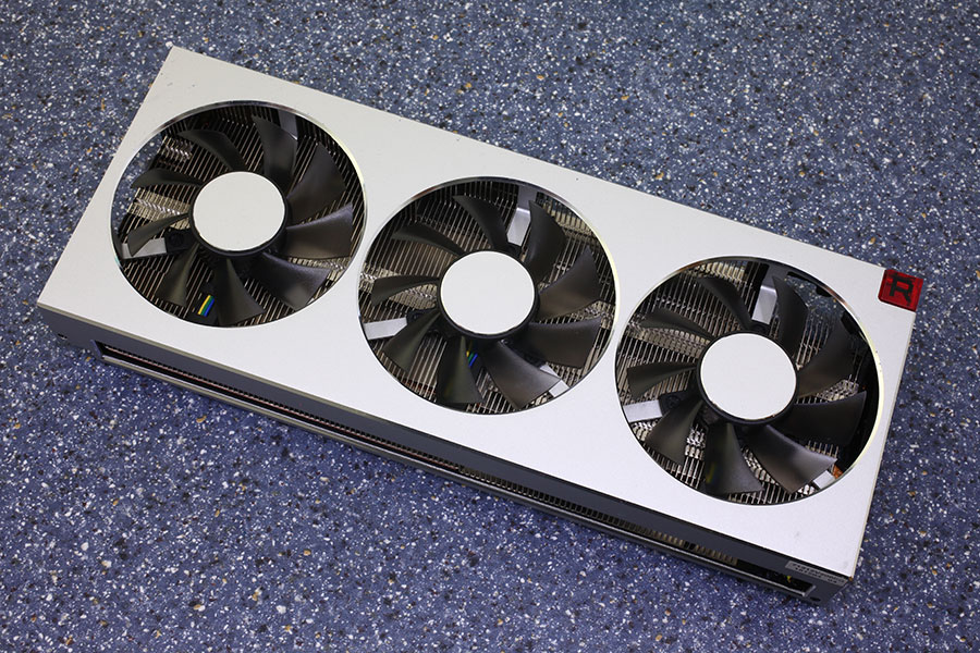
Radeon VII is the first high-end graphics card from AMD to feature a contemporary triple-fan aluminium heatsink reference cooler. The company has finally wised up to the realities of the axial blower cooler being way too loud and AIO liquid cooling solutions looking too clumsy. The company is also counting on the novelty value of the world's first 7 nm GPU to sell these cards.
In this review, we have with us an AMD Radeon VII graphics card, which is strictly reference-design. You'll be able to buy this card through AMD's various add-in board (AIB) partners—they'll all use the same physical design with only make minor changes, like stickers with their own branding.
| Price | Shader Units | ROPs | Core Clock | Boost Clock | Memory Clock | GPU | Transistors | Memory | |
|---|---|---|---|---|---|---|---|---|---|
| RTX 2060 FE | $350 | 1920 | 48 | 1365 MHz | 1680 MHz | 1750 MHz | TU106 | 10800M | 6 GB, GDDR6, 192-bit |
| GTX 1080 | $460 | 2560 | 64 | 1607 MHz | 1733 MHz | 1251 MHz | GP104 | 7200M | 8 GB, GDDR5X, 256-bit |
| RX Vega 64 | $400 | 4096 | 64 | 1247 MHz | 1546 MHz | 953 MHz | Vega 10 | 12500M | 8 GB, HBM2, 2048-bit |
| GTX 1080 Ti | $675 | 3584 | 88 | 1481 MHz | 1582 MHz | 1376 MHz | GP102 | 12000M | 11 GB, GDDR5X, 352-bit |
| RTX 2070 | $500 | 2304 | 64 | 1410 MHz | 1620 MHz | 1750 MHz | TU106 | 10800M | 8 GB, GDDR6, 256-bit |
| RTX 2070 FE | $600 | 2304 | 64 | 1410 MHz | 1710 MHz | 1750 MHz | TU106 | 10800M | 8 GB, GDDR6, 256-bit |
| Radeon VII | $700 | 3840 | 64 | 1400 MHz | 1750 MHz | 1000 MHz | Vega 20 | 13230M | 16 GB, HBM2, 4096-bit |
| RTX 2080 | $700 | 2944 | 64 | 1515 MHz | 1710 MHz | 1750 MHz | TU104 | 13600M | 8 GB, GDDR6, 256-bit |
| RTX 2080 FE | $800 | 2944 | 64 | 1515 MHz | 1800 MHz | 1750 MHz | TU104 | 13600M | 8 GB, GDDR6, 256-bit |
| RTX 2080 Ti FE | $1200 | 4352 | 96 | 1350 MHz | 1635 MHz | 1750 MHz | TU102 | 18600M | 11 GB, GDDR6, 352-bit |
| RTX 2080 Ti | $1300 | 4352 | 96 | 1350 MHz | 1545 MHz | 1750 MHz | TU102 | 18600M | 11 GB, GDDR6, 352-bit |
2nd Generation Vega Architecture


It may appear like the underlying architecture of Radeon VII is exactly the same as the RX Vega 64 from 2017, codenamed "Vega," but that's not entirely true. Radeon VII is based on what AMD refers to as "Enhanced 2nd Generation Vega architecture."
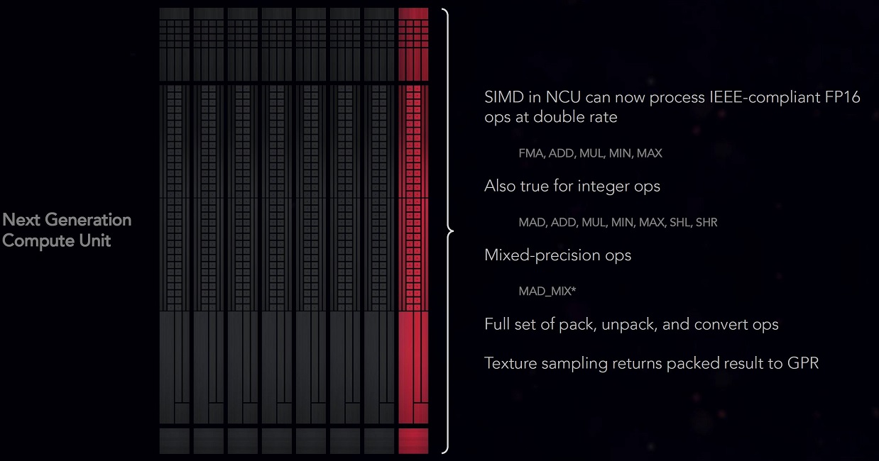
What's new are optimizations that increase frequency by tapping into the engine clock headroom dividend from the switch to 7 nm, reduced latencies across the silicon (think caches, memory controllers, buffers, etc.), increased bandwidth to the 64 ROPs, and notable changes to the "Vega" NGCU (next generation compute unit) that include additional integer and floating-point accumulators, which probably increases IPC a few percentage points.
AMD has also doubled down on the chip's power-management features, beginning with something it calls "Enhanced Thermal Monitoring." The company has sprinkled double the number of temperature sensors across the GPU die. Clock-speed control is now based on junction temperature, which represents data from a larger network of sensors that lets the GPU more accurately control its frequency and voltages, which translates to better sustainability of boost frequencies. This also means the GPU can throttle itself more accurately to maintain reliability of the silicon. AMD presented its own tests that show throttling based on junction temperature rather than edge temperature results in a two percent performance uplift due to better boost frequency sustainability.
The most obvious improvement, though, is the memory interface, which is 4096-bit wide, twice that of "Vega 10," which doubles the memory bandwidth. AMD also chose to equip the Radeon VII with 16 GB of HBM2 memory, doubling it from the previous generation.

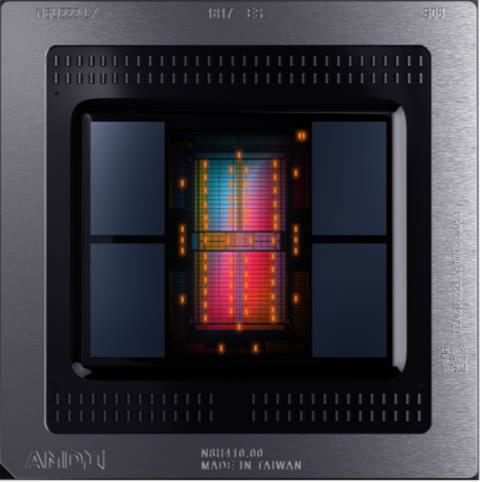
Much like the "Vega 10" that powers the RX Vega 64, the "Vega 20" GPU at the heart of the Radeon VII is a multi-chip module (MCM), a combination of the 7 nm GPU die, four 10 nm-class HBM2 memory stacks supplied by either SK Hynix or Samsung, and a silicon interposer on which the GPU and HBM2 stacks sit. The interposer enables high-density microscopic wiring between the GPU and memory stacks, while TSVs (through silicon vias) connect the GPU and memory stacks to the fiberglass package substrate underneath. The switch to 7 nm has reduced the die-size of the GPU from 495 mm² on the 14 nm "Vega 10" down to 331 mm², which isn't half, but one should realize that "Vega 20" isn't an optical-shrink as there are numerous physical changes to the die which we described above.
Barring small changes to the NGCUs, as lower-latency caches and additional accumulators for both the integer and floating-point sides, the number-crunching resources of "Vega 20" and the chip's hierarchy is essentially the same. The GPU physically features 64 NGCUs, although only 60 of them are enabled on the Radeon VII. This is probably done to increase yields/harvesting of the silicon. These 60 NGCUs amount to 3,840 stream processors and 240 TMUs. The ROP count is unchanged at 64, although AMD has increased the bandwidth of these ROPs. The memory bus width has doubled to 4096-bit, as has the memory amount at 16 GB.
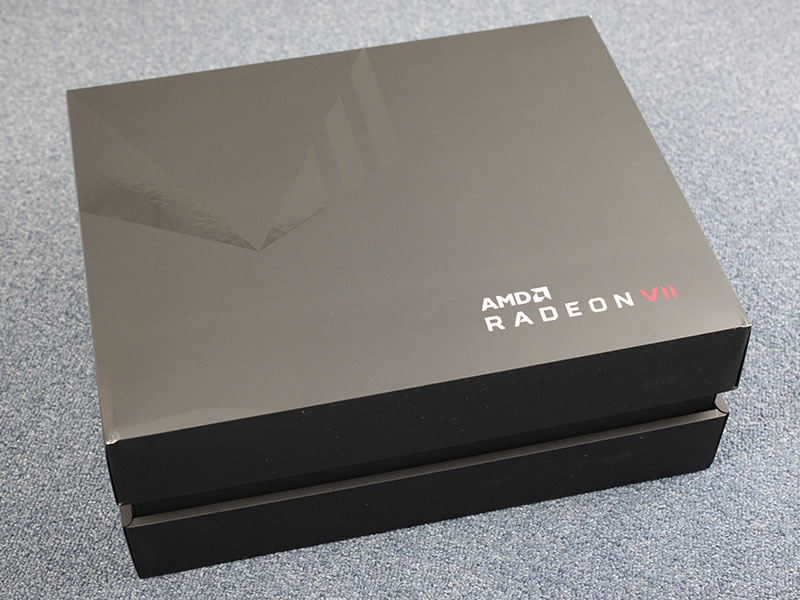
Packaging and Contents
Additional impressions of the package and the card are available in our unboxing and preview article we posted a few days ago.
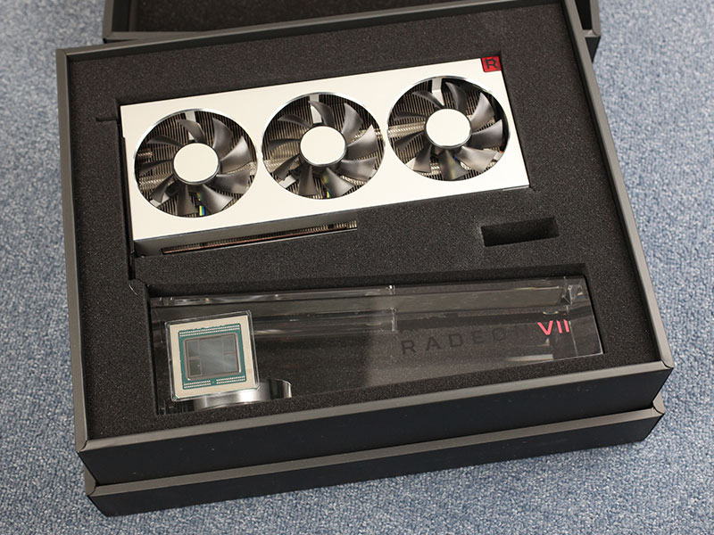
You will receive:
- Graphics card
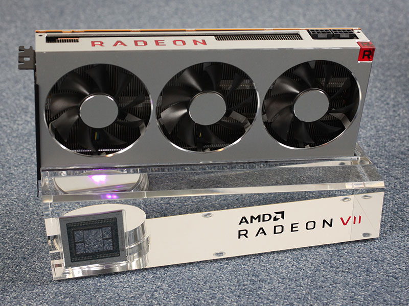
- LED-lit stand to show off the graphics card (batteries included)
- Vega 20 GPU

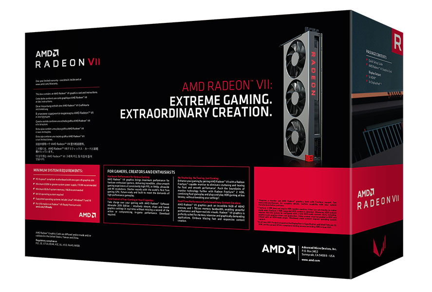
This seems to be a special reviewer-only package—actual retail cards will come in the packaging displayed above, with the usual accessories, like a driver disc and documentation.
The Card


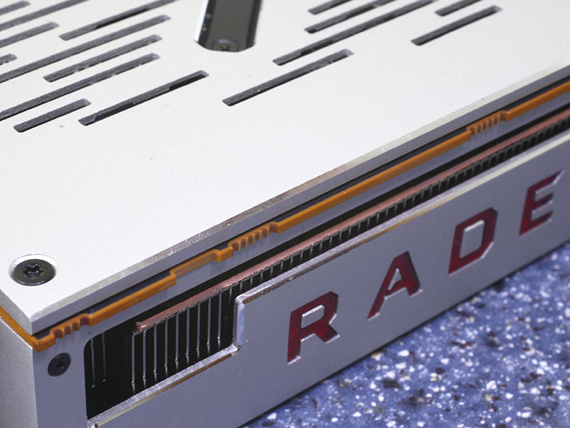
The Radeon VII comes in an aluminium-clad design that's dominated by brushed metal surfaces, which give the card a high-quality premium look and feel. This is the first time an AMD reference design comes with three fans to maximize airflow. The metal backplate matches the visual theme of the main cooler. Dimensions of the card are 27.0 x 12.0 cm, which ensures it will fit nearly all cases except for the most compact ones.
Installation requires two slots in your system.

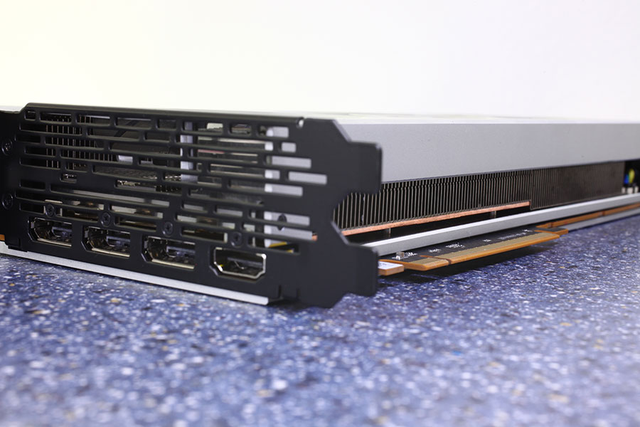
Display connectivity options include three standard DisplayPort 1.4a and one HDMI 2.0b port. This is the same output configuration as on Vega 56 and Vega 64.
The HDMI port is version 2.0, and DisplayPort uses 1.4 HBR3, MST, and HDR. This enables support for 4K @ 120 Hz, 5K @ 60 Hz, or 8K @ 60 Hz. Supported HDR configurations are 4K60, 4K120, and 5K60, just like first-generation Vega. GPU-accelerated encoding is capable of HEVC/H.264 at up to 1080p240, 1440p120, and 2160p60. Hardware-based decoding works at up to 4K60 for H.264, H.265, and VP9 (shader-assisted).

The board uses two 8-pin power connectors. This input configuration is specified for up to 375 watts of power draw.
AMD CrossFire has been running over the PCI-Express bus for a few generations now. The Vega Series is no different.
Disassembly
Once the backplate is removed, the main cooling assembly comes off easily. The whole disassembly process is fairly straightforward and much easier than on the NVIDIA RTX 2070 or RTX 2060.
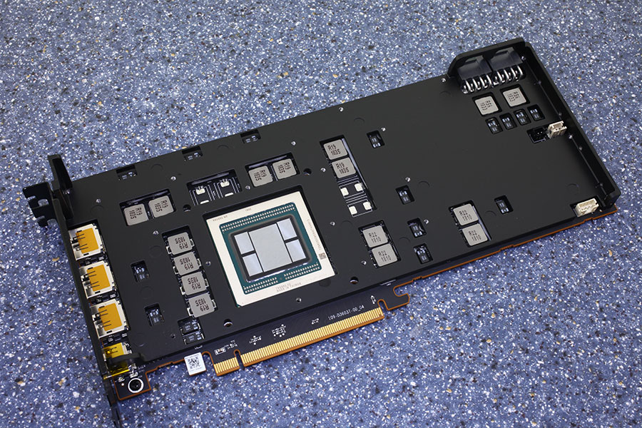


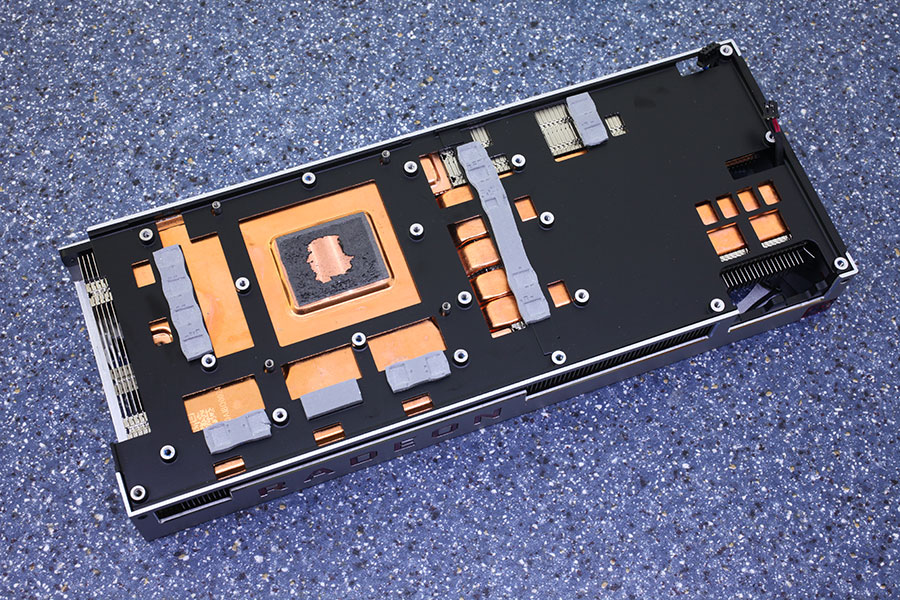
Only after finishing the full disassembly did I notice that there are actually two pieces that make up the main cooler: a black metal baseplate that cools voltage regulation circuitry and the main heatsink with the copper baseplate, heatpipes, and three fans attached to it.

Note the black thermal pad AMD is using. It's of a fairly solid substance that's sticky and really difficult to get off unless you dissolve it (I used ArctiClean). It's also interesting how the thermal pad broke when the cooler came off—it is definitely not reusable. It looks like it got more sticky at the hottest spot (in the center of the GPU die), so the outer areas stuck with the cooler while the center part stuck to the GPU chip. After a bit of research, it looks like the pad is a Hitachi TC-HM03 and uses a mix of graphite strands (pure carbon) and epoxy to create a thick, reusable, high conductivity thermal pad. I'm not 100% sure why AMD went with this instead of traditional thermal paste. The GPU surface, including the HBM chips, seems perfectly flat, unlike some earlier Vega 10 cards where height differences had to be filled out by thermal paste.
In the overclocking section of this review, we'll also describe how we significantly improved thermal performance by using regular paste with increased mounting pressure.

Once cleaned up, you can see the large copper vapor-chamber that soaks up heat from the GPU surface and the five heatpipes attached to it. These heatpipes spread heat to the edges of the fin-stack.

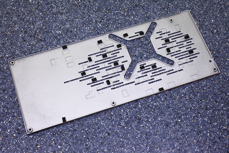
The backplate is made out of metal and protects the card against damage during installation and handling.
On the next page, we dive deep into the PCB layout and VRM configuration.
Our Patreon Silver Supporters can read articles in single-page format.
Mar 13th, 2025 03:05 EDT
change timezone
Latest GPU Drivers
New Forum Posts
- The future of RDNA on Desktop. (126)
- RX 9070 availability (223)
- Nvidia's GPU market share hits 90% in Q4 2024 (gets closer to full monopoly) (907)
- What's your latest tech purchase? (23290)
- How's your old spinner holding up? (47)
- Shadow of the Tomb Raider benchmark (541)
- HTTP request has timed out (8)
- X79 and/or rampage IV OC'ing thread for those of us still left.... (2389)
- User Error Fail - PS5 (6)
- aio fan droplets (24)
Popular Reviews
- AMD Ryzen 9 9950X3D Review - Great for Gaming and Productivity
- XFX Radeon RX 9070 XT Mercury OC Magnetic Air Review
- Sapphire Radeon RX 9070 XT Nitro+ Review - Beating NVIDIA
- Dough Spectrum Black 32 Review
- FSP MP7 Black Review
- ASUS Radeon RX 9070 TUF OC Review
- AMD Ryzen 7 9800X3D Review - The Best Gaming Processor
- NVIDIA GeForce RTX 5070 Founders Edition Review
- ASUS GeForce RTX 5090 TUF Review
- MSI MAG B850 Tomahawk Max Wi-Fi Review
Controversial News Posts
- NVIDIA GeForce RTX 50 Cards Spotted with Missing ROPs, NVIDIA Confirms the Issue, Multiple Vendors Affected (513)
- AMD Radeon RX 9070 and 9070 XT Listed On Amazon - One Buyer Snags a Unit (261)
- AMD RDNA 4 and Radeon RX 9070 Series Unveiled: $549 & $599 (260)
- AMD Mentions Sub-$700 Pricing for Radeon RX 9070 GPU Series, Looks Like NV Minus $50 Again (249)
- NVIDIA Investigates GeForce RTX 50 Series "Blackwell" Black Screen and BSOD Issues (244)
- AMD Radeon RX 9070 and 9070 XT Official Performance Metrics Leaked, +42% 4K Performance Over Radeon RX 7900 GRE (195)
- AMD Radeon RX 9070-series Pricing Leaks Courtesy of MicroCenter (158)
- AMD Radeon RX 9070 XT Reportedly Outperforms RTX 5080 Through Undervolting (101)