 66
66
ASRock Radeon RX 6900 XT OC Formula Review - This Card is Fast
Test Setup »High-resolution PCB Pictures
These pictures are for the convenience of volt modders and people who would like to see all the finer details on the PCB. Feel free to link back to us and use these in your articles, videos or forum posts.
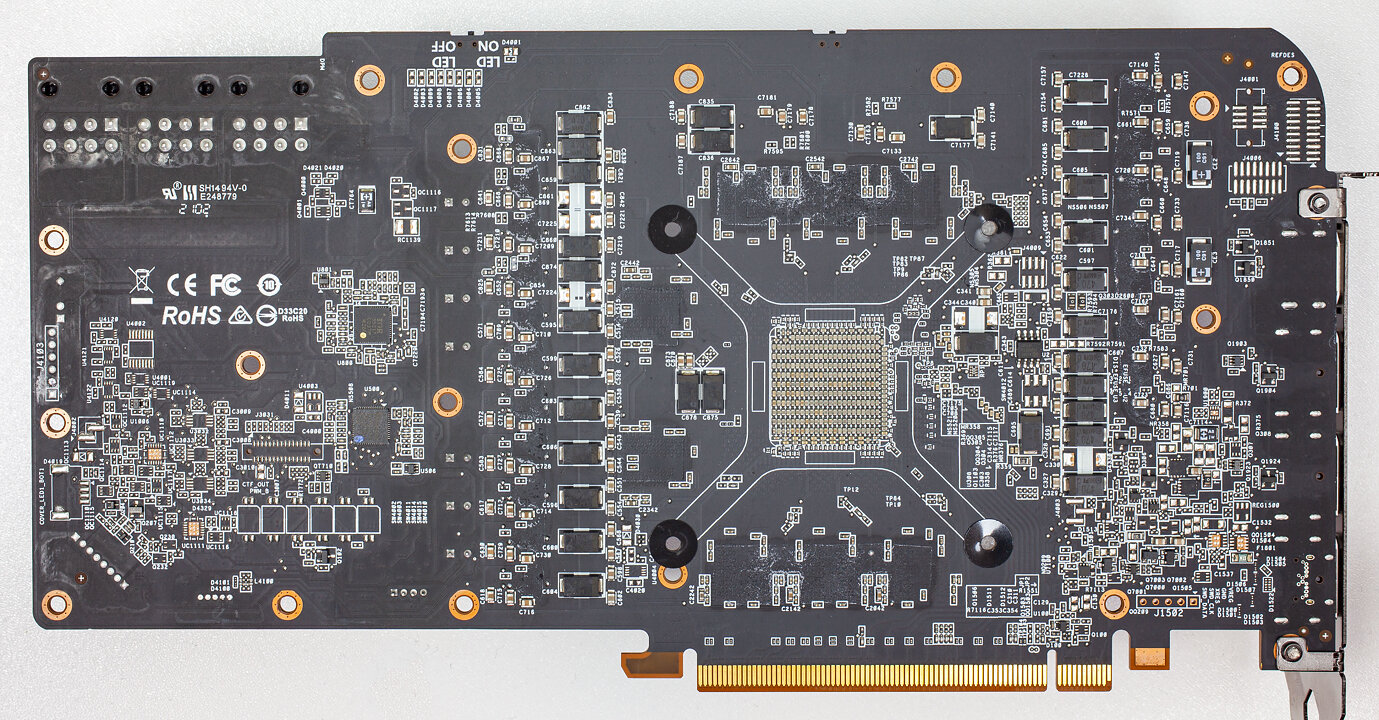
High-res versions are also available (front, back).
Circuit Board (PCB) Analysis
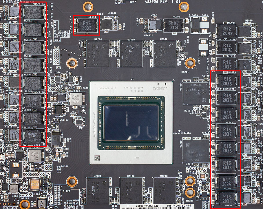
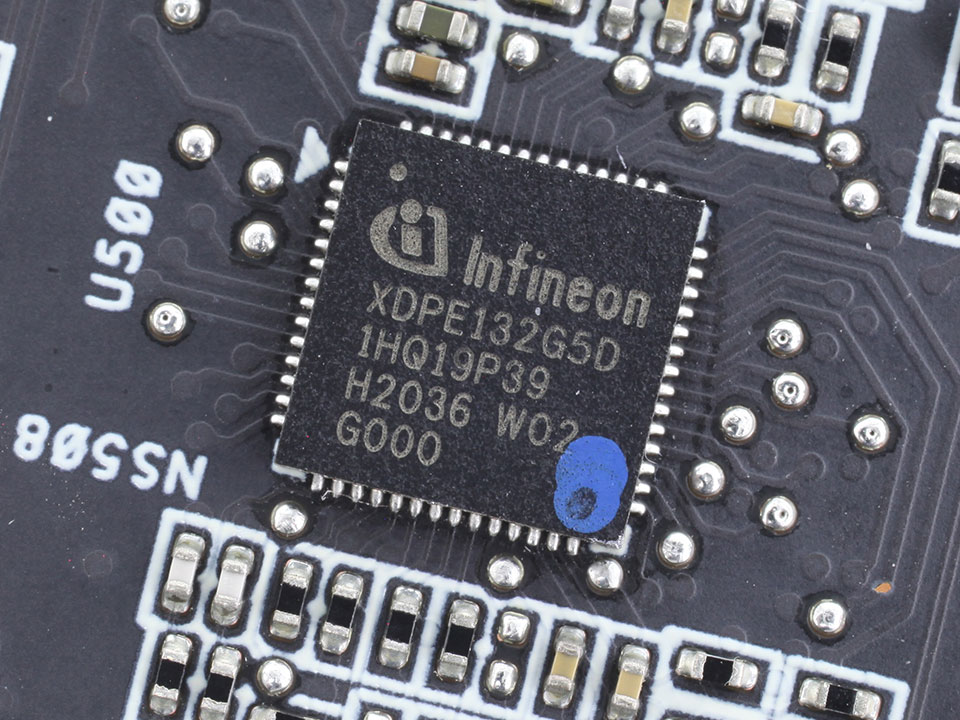
GPU voltage is powered by the expensive Infineon XDPE132G5D running 17 power phases.
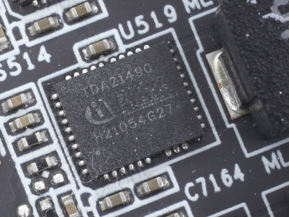
International Rectifier TDA21490 DrMOS chips are used for GPU voltage. Note that these are rated for 90 A, whereas the chips on other RX 6900 XT cards are rated for 72 A only.
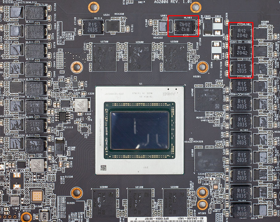
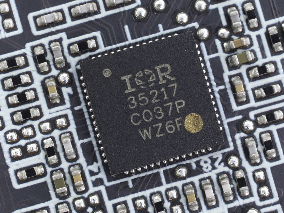
Memory voltage uses a four-phase design and is generated by an IRF35217 controller.
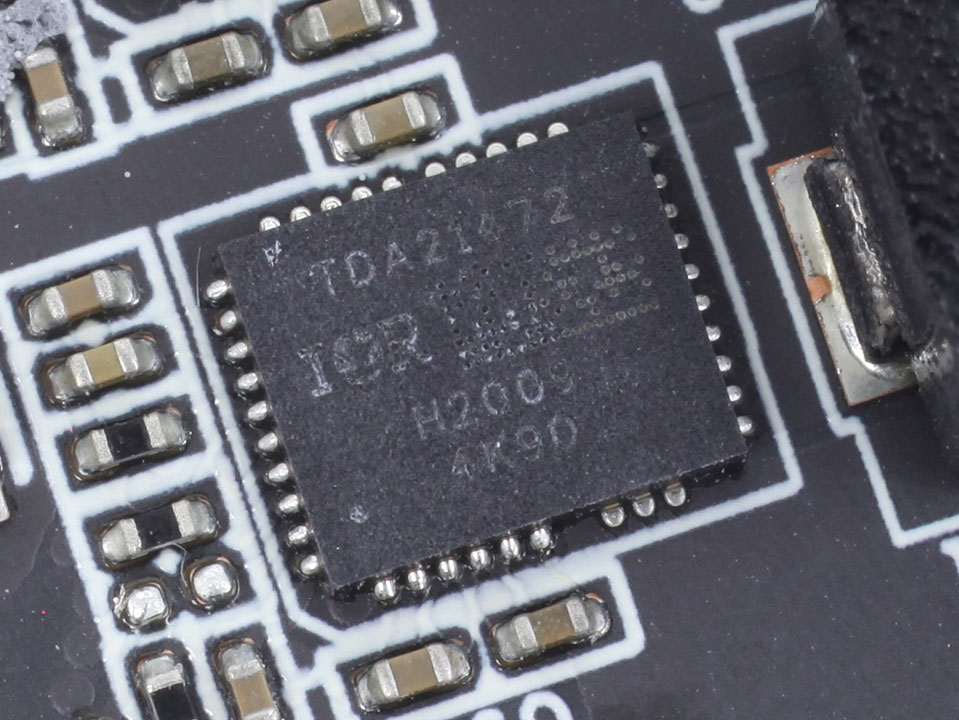
For memory, TDA21472 DrMOS chips are used.
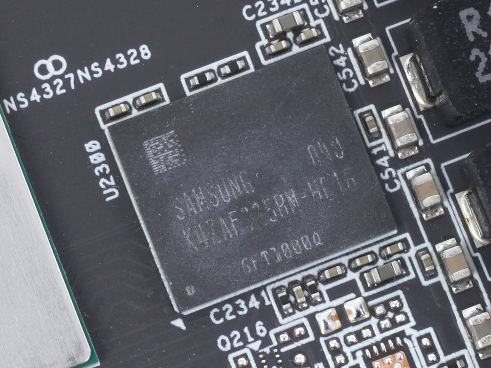
GDDR6 chips are made by Samsung, carry the model number "K4ZAF325BM-HC16," and are rated to run at 16 Gbps.
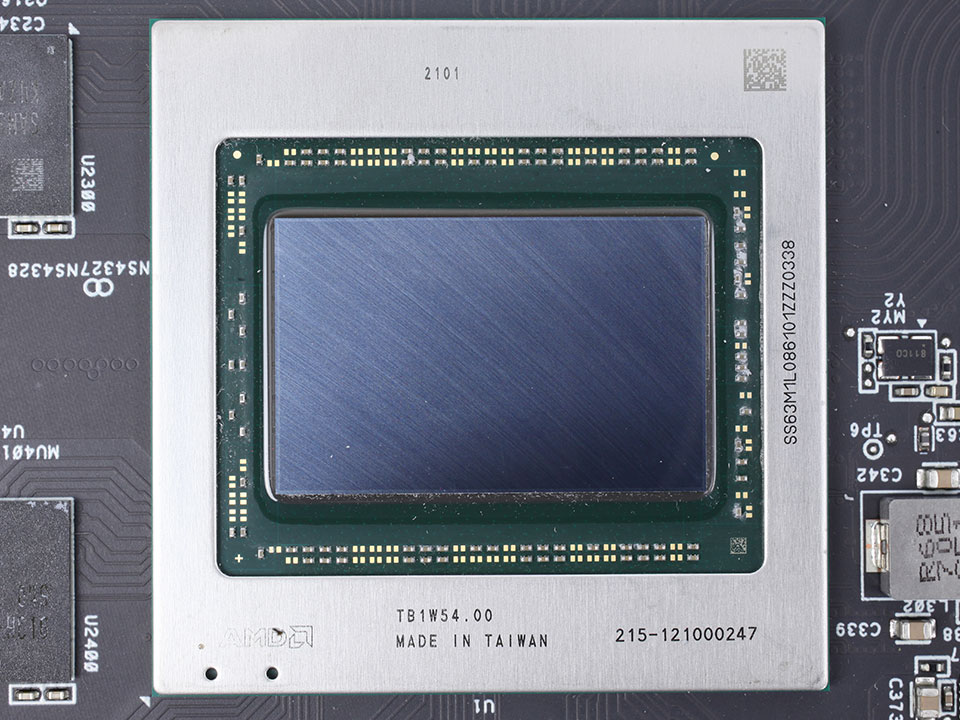
Built on the same TSMC N7 (7 nm) node as Navi 10, the Navi 21 silicon is spread across a 519.8 mm² die area and packs 26.8 billion transistors. The pinkish-red tinge we saw on Navi 10 is gone.
May 4th, 2025 08:31 EDT
change timezone
Latest GPU Drivers
New Forum Posts
- Milestones (14020)
- WCG Daily Numbers (12858)
- Post Your CyberPunk 2077 Benchmark (2024 edition) (124)
- Old NVIDIA GPU with torn branding sticker - what’s the brand? (5)
- TPU's Rosetta Milestones and Daily Pie Thread (2299)
- Ssd failure, I don’t know what to do (27)
- Free Games Thread (4658)
- Are the 8 GB cards worth it? (815)
- Technical Issues - TPU Main Site & Forum (2025) (167)
- TPU's WCG/BOINC Team (34499)
Popular Reviews
- Clair Obscur: Expedition 33 Performance Benchmark Review - 33 GPUs Tested
- ASUS ROG Maximus Z890 Hero Review
- ASUS Radeon RX 9070 XT TUF OC Review
- Montech HS02 PRO Review
- NVIDIA GeForce RTX 5060 Ti 8 GB Review - So Many Compromises
- ASUS GeForce RTX 5090 Astral Liquid OC Review - The Most Expensive GPU I've Ever Tested
- Seasonic Vertex GX 850 W Review
- Upcoming Hardware Launches 2025 (Updated Apr 2025)
- ASRock Radeon RX 9070 XT Taichi OC Review - Excellent Cooling
- Team Group GC Pro 2 TB Review
Controversial News Posts
- NVIDIA GeForce RTX 5060 Ti 16 GB SKU Likely Launching at $499, According to Supply Chain Leak (182)
- AMD Radeon RX 9060 XT to Roll Out 8 GB GDDR6 Edition, Despite Rumors (129)
- NVIDIA Sends MSRP Numbers to Partners: GeForce RTX 5060 Ti 8 GB at $379, RTX 5060 Ti 16 GB at $429 (128)
- NVIDIA Launches GeForce RTX 5060 Series, Beginning with RTX 5060 Ti This Week (115)
- Nintendo Confirms That Switch 2 Joy-Cons Will Not Utilize Hall Effect Stick Technology (105)
- NVIDIA PhysX and Flow Made Fully Open-Source (95)
- Sony Increases the PS5 Pricing in EMEA and ANZ by Around 25 Percent (84)
- Parts of NVIDIA GeForce RTX 50 Series GPU PCB Reach Over 100°C: Report (78)