 5
5
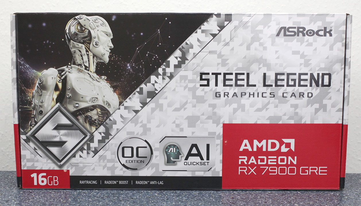
ASRock Radeon RX 7900 GRE Steel Legend Review
(5 Comments) »Introduction
ASRock Radeon RX 7900 GRE Steel Legend is a premium custom design graphics card based on the not-so-new RX 7900 GRE, which is seeing a wider launch today. The RX 7900 GRE was originally launched as a China-exclusive product back in July 2023. It stayed in the market over the months, and AMD has found a new mission for it—competing with the GeForce RTX 4070 Super, and so it was just a matter of scaling up the production of this card, and having it shipped to certain markets outside China. The January 2024 introduction of the RTX 4070 Super and RTX 4070 Ti Super, and their impact on the real-world prices of the RTX 4070 and RTX 4070 Ti, is what set the ball in motion for today's wider launch of the RX 7900 GRE.

AMD carved the RX 7900 GRE out of the Navi 31 silicon powering the other RX 7900 series cards, such as the RX 7900 XT and RX 7900 XTX, but this is the compacted Navi 31 package AMD originally designed for the mobile RX 7900 series GPUs. This package has a lower pin-count, with pins for just a 256-bit wide memory bus; and fewer power pins. We could be wrong, but the compact Navi 31 and Navi 32 could be sharing a pin-map, which makes the former compatible with PCBs AMD and its partners originally designed for the RX 7800 XT, which are simpler, and hence more cost-effective.
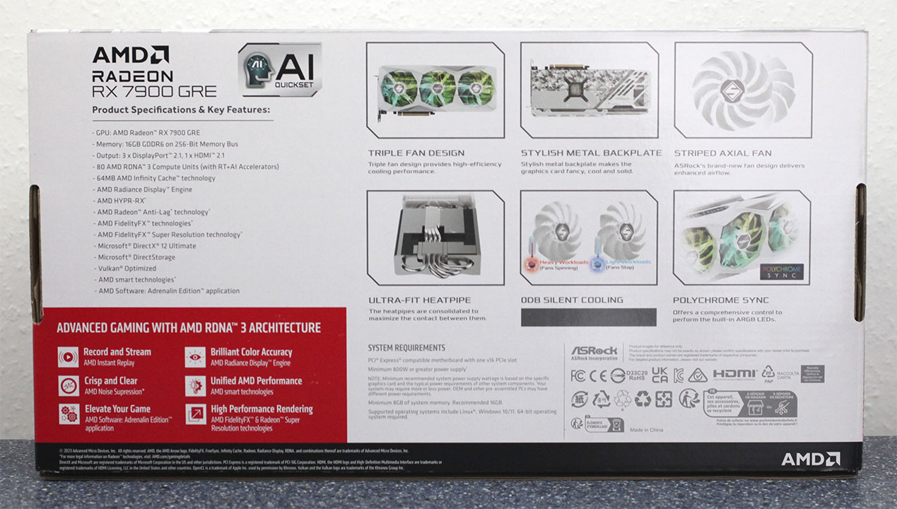
To create the RX 7900 GRE, AMD enabled 80 out of 96 compute units (CU) present on the Navi 31 graphics compute die (GCD), to result in 5,120 stream processors, 160 AI accelerators, 80 Ray accelerators, and 320 TMUs—somewhat similar counts to the RX 6950 XT, but on a newer architecture. 160 out of 192 ROPs are enabled. The memory sub-system sees a 256-bit memory bus drive 16 GB of 18 Gbps GDDR6 memory for 576 GB/s of bandwidth on tap—same as the RX 6950 XT. What sets the RX 7900 XT apart from this card is the wider 320-bit memory bus driving 20 GB of faster 20 Gbps memory for 38% more bandwidth; besides 4 extra CU.
The RDNA 3 graphics architecture powering the RX 7900 GRE introduces new dual-issue rate compute units, with vastly improved idle SIMD resource utilization, and support for new math formats. The company claims generational IPC uplifts over the RDNA 2 compute units to the tune of 17%. Taking advantage of the newer 5 nm node, AMD is also running the shader engines at higher clock speeds than the previous generation. The company also introduced Ray Accelerator, a component inside the CU that accelerates matrix math functions by utilizing the SIMD units, which should accelerate AI DNN building and training. The second generation Ray Accelerator is designed to provide a 50% generational improvement in ray intersection performance. Another interesting change introduced with RDNA 3 is that the GPU's front-end operates at a 10-15% higher clock speed than the shader engines.
The ASRock RX 7900 GRE Steel Legend is a slick new white-themed trim. In its product stack, the Steel Legend is positioned between the Challenger OC and Phantom Gaming SKUs. Besides a triple-slot cooling solution, you get multicolor LED lighting for the card's trio of fans; and a slight factory overclock. According to ASRock, the Steel Legend is priced at $570, a small $20 increase over the AMD MSRP.
Short 10-Minute Video Summary Comparing 6x RX 7900 GRE
Our goal with the videos is to create short summaries, not go into all the details and test results, which can be found in this written review.
| Price | Cores | ROPs | Core Clock | Boost Clock | Memory Clock | GPU | Transistors | Memory | |
|---|---|---|---|---|---|---|---|---|---|
| RTX 3070 | $310 | 5888 | 96 | 1500 MHz | 1725 MHz | 1750 MHz | GA104 | 17400M | 8 GB, GDDR6, 256-bit |
| RTX 3070 Ti | $350 | 6144 | 96 | 1575 MHz | 1770 MHz | 1188 MHz | GA104 | 17400M | 8 GB, GDDR6X, 256-bit |
| RX 6800 | $450 | 3840 | 96 | 1815 MHz | 2105 MHz | 2000 MHz | Navi 21 | 26800M | 16 GB, GDDR6, 256-bit |
| RX 7700 XT | $430 | 3456 | 96 | 2171 MHz | 2544 MHz | 2250 MHz | Navi 32 | 26500M | 12 GB, GDDR6, 192-bit |
| RX 6800 XT | $500 | 4608 | 128 | 2015 MHz | 2250 MHz | 2000 MHz | Navi 21 | 26800M | 16 GB, GDDR6, 256-bit |
| RTX 3080 | $450 | 8704 | 96 | 1440 MHz | 1710 MHz | 1188 MHz | GA102 | 28000M | 10 GB, GDDR6X, 320-bit |
| RTX 4070 | $525 | 5888 | 64 | 1920 MHz | 2475 MHz | 1313 MHz | AD104 | 35800M | 12 GB, GDDR6X, 192-bit |
| RX 7800 XT | $500 | 3840 | 96 | 2124 MHz | 2430 MHz | 2425 MHz | Navi 32 | 28100M | 16 GB, GDDR6, 256-bit |
| RX 6900 XT | $650 | 5120 | 128 | 2015 MHz | 2250 MHz | 2000 MHz | Navi 21 | 26800M | 16 GB, GDDR6, 256-bit |
| RX 6950 XT | $630 | 5120 | 128 | 2100 MHz | 2310 MHz | 2250 MHz | Navi 21 | 26800M | 16 GB, GDDR6, 256-bit |
| RTX 3090 | $800 | 10496 | 112 | 1395 MHz | 1695 MHz | 1219 MHz | GA102 | 28000M | 24 GB, GDDR6X, 384-bit |
| RTX 4070 Super | $590 | 7168 | 80 | 1980 MHz | 2475 MHz | 1313 MHz | AD104 | 35800M | 12 GB, GDDR6X, 192-bit |
| RX 7900 GRE | $550 | 5120 | 160 | 1880 MHz | 2245 MHz | 2250 MHz | Navi 31 | 57700M | 16 GB, GDDR6, 256-bit |
| ASRock RX 7900 GRE Steel Legend | $570 | 5120 | 160 | 1972 MHz | 2333 MHz | 2250 MHz | Navi 31 | 57700M | 16 GB, GDDR6, 256-bit |
| RTX 4070 Ti | $720 | 7680 | 80 | 2310 MHz | 2610 MHz | 1313 MHz | AD104 | 35800M | 12 GB, GDDR6X, 192-bit |
| RTX 4070 Ti Super | $800 | 8448 | 96 | 2340 MHz | 2610 MHz | 1313 MHz | AD103 | 45900M | 16 GB, GDDR6X, 256-bit |
| RX 7900 XT | $700 | 5376 | 192 | 2000 MHz | 2400 MHz | 2500 MHz | Navi 31 | 57700M | 20 GB, GDDR6, 320-bit |
| RTX 3090 Ti | $1050 | 10752 | 112 | 1560 MHz | 1950 MHz | 1313 MHz | GA102 | 28000M | 24 GB, GDDR6X, 384-bit |
| RTX 4080 | $1200 | 9728 | 112 | 2205 MHz | 2505 MHz | 1400 MHz | AD103 | 45900M | 16 GB, GDDR6X, 256-bit |
| RTX 4080 Super | $1300 | 10240 | 112 | 2295 MHz | 2550 MHz | 1438 MHz | AD103 | 45900M | 16 GB, GDDR6X, 256-bit |
| RX 7900 XTX | $910 | 6144 | 192 | 2300 MHz | 2500 MHz | 2500 MHz | Navi 31 | 57700M | 24 GB, GDDR6, 384-bit |
| RTX 4090 | $1850 | 16384 | 176 | 2235 MHz | 2520 MHz | 1313 MHz | AD102 | 76300M | 24 GB, GDDR6X, 384-bit |
AMD RDNA 3 Graphics Architecture


The Radeon RX 7900 series debuts AMD's third generation RDNA graphics architecture, termed RDNA 3. With it, AMD plans to repeat the generational 50% performance/Watt gain it achieved with RDNA 2, which sprung it back to the high-end graphics segment after a long gap. AMD claims it succeeded in this endeavor, with a 54% generational performance/Watt gain. At the heart of this effort is the switch to the new TSMC 5 nm EUV foundry node. AMD figured out early on that it cannot build large monolithic GPUs on 5 nm without thinning its margins in the fight against NVIDIA, and set out to innovate the Chiplet architecture for the GPU. Under this, specific parts of the GPU that actually benefit from a switch to a newer foundry node, such as the Shader Engines, would be built on a centralized 5 nm die called the Graphics Compute Die (GCD), while those components that can make do with a less advanced node, namely the memory controllers and L3 cache, would be spun off to chiplets called Memory Cache Dies (MCDs), built on 6 nm.

The "Navi 31" GPU is hence a chiplet GPU and not a multi-chip module like "Vega 10." In a chiplet-based device, various components that can otherwise not exist on their own packages, are placed on a single package, with the goal of minimizing production costs, by stratifying their need for a new foundry node, such that only the most power-intensive IP receive the most advanced node. In a MCM, chips that can otherwise exist on their own package, are combined onto a single package for conserving PCB real-estate, or reducing latency. The GCD in the "Navi 31" GPU hence has all the shader engines, caches up to L2, the front-end Command Processor, Async Compute Engines (ACEs), the Display Engine, and the Media Engine. Each of the six MCDs has a 64-bit wide memory bus, and a 16 MB segment of the GPU's 96 MB Infinity Cache memory. The size of the Infinity Cache may have been generationally reduced (compared to 128 MB on "Navi 21"), but AMD has widened the memory bus itself, from 256-bit up to 384-bit.
Much of the architectural innovation is not with the chiplet design (a packaging innovation); but at the level of the RDNA 3 Dual-Compute Unit (or Compute Unit pair). The "Navi 31" GPU physically features 96 compute units spread across six Shader Engines. AMD claims that at the same engine clocks, the RDNA 3 CU offers a 17.4% IPC increase over the RDNA 2 CU. There are 20% more CUs over the "Navi 21," and these run at higher engine clocks, tapping into the power headroom afforded by the 5 nm process. These combined work out to the 54% generational performance uplift, with which AMD plans to retain competitiveness with NVIDIA's RTX 40-series "Ada" high-end SKUs.


The new RDNA 3 CU introduces multi-precision capability for the 64 stream processors per CU: operating either as 1x SIMD64 or 2x SIMD32 units. The Vector Unit that houses these SIMD units can either function as a SIMD execution mechanism, or as a Matrix execution unit, thanks to the new AI Matrix Accelerator, which provides a 2.7x matrix multiplication performance uplift versus conventional SIMD execution. Also added are support for the Bfloat16 instruction-set, and SIMD8 execution. The GPU hence enjoys AI hardware-acceleration that can be leveraged in future feature-additions relevant to gamers, such as FSR 3.0. Game developers will also look for ways to exploit accelerated AI, now that all three brands feature it (NVIDIA Tensor cores and Intel XMX cores).


AMD's first-generation Ray Accelerator, introduced with the RDNA 2 architecture, was the result of a hasty effort to catch up to NVIDIA with a DirectX 12 Ultimate GPU, where they developed a fixed-function hardware to calculate ray intersections, and offloaded a large chunk of RT processing to the generationally-doubled SIMD resources. With RDNA 3, they've refined the Ray Accelerator to achieve an 80% ray tracing performance uplift over the previous generation, when you add up the Ray Accelerator count, their higher engine clocks, and other hardware-level optimizations, such as early subtree culling, specialized box sorting modes, and reduced traversal iterations.


There is a 50% ray intersection capacity improvement for the "Navi 31" GPU thanks to these optimizations, and cycles-per-ray reduction. Besides these, AMD has also made several improvements to the geometry- and pixel-pipes, with the introduction of the new multi-draw indirect accelerator (MDIA), which reduces CPU API and driver-level overheads by gathering and parsing of multi-draw command data. At the hardware-level 12 primitives per clock is now supported compared to 8 per clock on RDNA 2, thanks to culling. The core-configuration overall enables 50% more rasterized performance per clock.
The GCD features six Shader Engines, each with 16 compute units (or 8 dual compute units), which work out to 1,024 stream processors. Six such Shader Engines make up 6,144 stream processors with 96 Ray Accelerators and 96 AI Accelerators. The GPU has 384 TMUs, and a massive 192 ROPs—a 50% increase over "Navi 21." The Radeon RX 7900 XTX enables all 96 CUs, and maxes out the silicon, whereas the RX 7900 XT has 84 out of 96 CUs enabled, which work out to 5,376 stream processors, 84 Ray Accelerators, 336 TMUs, and an unchanged 192 ROPs. The new RX 7900 GRE has 80 CUs enabled, which work out to 5,120 stream processors, 80 Ray Accelerators, 320 TMUs, and 160 ROPs. The RX 7900 XTX gets 24 GB of GDDR6 memory across the GPU's entire 384-bit memory bus, with a memory speed of 20 Gbps (GDDR6-effective), which means 960 GB/s of memory bandwidth. The RX 7900 XT is equipped with 20 GB of memory across a narrower 320-bit memory bus carved out by disabling one of the six MCDs. At the same 20 Gbps speed, this yields 800 GB/s bandwidth. The RX 7900 GRE goes one further step down, with two of the six MCDs being disabled, for a 256-bit memory bus, running 16 GB of memory at 18 Gbps speed, for 576 GB/s of bandwidth.


AMD has significantly improved the Display Engine of "Navi 31" over the previous-generation in terms of connectivity. The new Radiance Display Engine comes with native support for DisplayPort 2.1, which enables 8K output at up to 165 Hz refresh-rate, or 4K at up to 480 Hz, with a single cable. AMD has refined its FSR 2 algorithm to support 8K (i.e. render at a lower resolution with FSR-enhanced upscaling), to make it possible to enjoy the latest AAA titles at playable frame-rates on 8K displays. All the RX 7900 series cards get two full-size DP 2.1 connectors, besides an HDMI 2.1b, and a USB-C with DP 1.2 passthrough. The "Navi 31" silicon receives full hardware-accelerated AV1 encode and decode capabilities, through dual independent encode/decoders, so two independent video streams can be simultaneously transcoded, or one stream at twice the framerate. With this generation, AMD is also introducing SmartAccess Video, a feature that lets the AMD driver leverage the hardware encoders of the RDNA 2 iGPU of Ryzen 7000 desktop processors, for additional encoding performance.
FidelityFX SuperResolution 3 Fluid Motion Frames (FSR 3 and FMF)

AMD announced the much awaited FidelityFX Super Resolution 3 and Fluid Motion Frames. FSR 3 is being announced as a technological rival to NVIDIA DLSS 3 Frame Generation. The premise with both technologies is the same—to effectively double frame-rates by generating alternate frames without running them through the entire graphics rendering pipeline, it's just that the two technologies differ in their approach to this goal.
FSR 3 builds on FSR 2 with its updated super resolution upscaler promising generational quality improvements at every given rendering resolution. Fluid Motion Frames (FMF) isn't the entirety of the FSR 3 feature-set, but is its most important feature-addition. FMF is a frame interpolation technology much like the one consumer televisions come with. Alternate frames are generated as an approximate of two frames. Where FMF differs from DLSS 3 Frame Generation is that while NVIDIA uses a hardware component called optical flow accelerator and the GPU's AI acceleration to generate an intermediate frame without involving the graphics rendering pipeline, FMF uses a certain amount of the graphics rendering pipeline. At a hardware level, FMF uses the main SIMD machinery of the GPU, leveraging asynchronous compute. As with DLSS 3 FG, FSR 3 FMF comes with added latency. NVIDIA counteracts this with Reflex, while AMD uses Radeon AntiLag+. Both technologies try to keep the frame queue short to reduce whole system latencies.
One major advantage FSR 3 FMF enjoys over DLSS 3 FG is that it works on any modern DirectX 12 GPU that supports async compute, since it doesn't require a specific hardware component the way DLSS 3 FG requires the Optical Flow Accelerator on NVIDIA "Ada" GPUs. The only limiting factor here is the performance. To be more specific, AMD says that all Radeon GPUs from RX 5700 series onward; and all GeForce GPUs from RTX 20-series onward, should support FSR 3 FMF. Also, FSR 3 FMF is as easy to integrate with games as FSR 2 is. The first games implementing FSR 3 FMF should arrive in Fall 2023. AMD is also working to extend FMF to Radeon Super Resolution, the driver-level technology that enables performance upscaling to even games that don't support FSR.
HYPR-RX
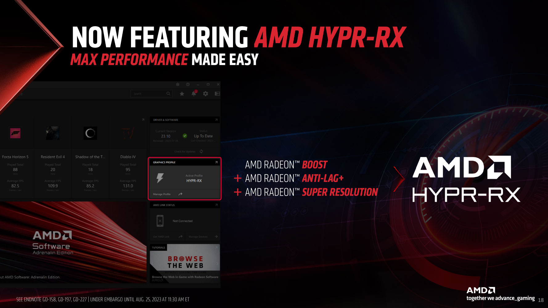
HYPR-RX is an interesting new feature in the AMD Software (control center) application. It is a one-click performance boosting technology that works with any DirectX 11 or DirectX 12 game. The software is a cocktail of Radeon Boost, Radeon AntiLag+, and Radeon Super Resolution, and applies the three features on any running game as needed, automatically. Radeon Boost improves performance by dynamically reducing the render resolution of a game when there's too much motion on the screen (and hence not enough detail needed). Radeon Super Resolution improves frame-rates as it applies FSR on the output of a game rendered at a lower resolution (including the frames lowered in resolution by Radeon Boost. AntiLag+ counteracts the latency added by these two, by shortening the frame queue. AFMF is part of the HYPR-RX feature-set, which can be activated with a single click.
Packaging
The Card
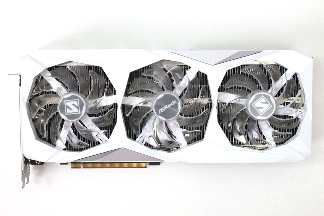
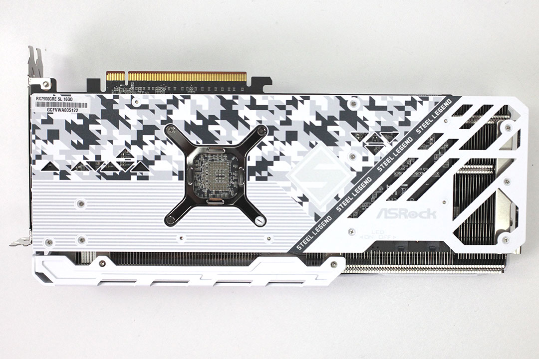
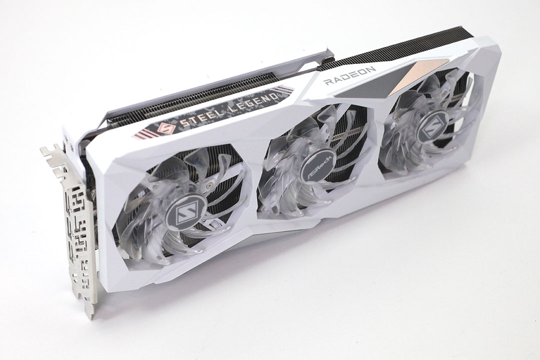
The unique selling point of the ASRock Steel Legend is its white color theme. ASRock added some gray highlights on the back, which look good. The cooler shroud is made of plastic, but the backplate is metal.
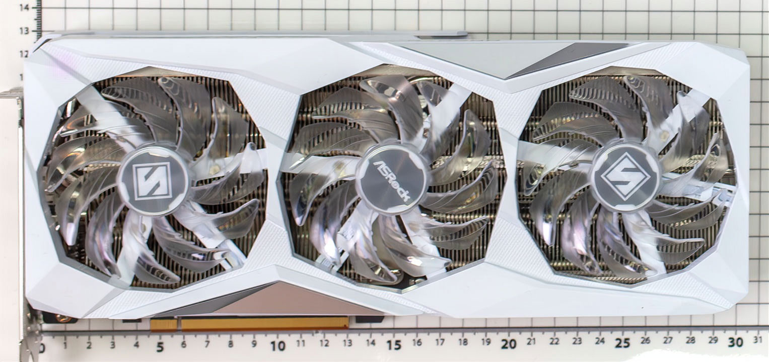
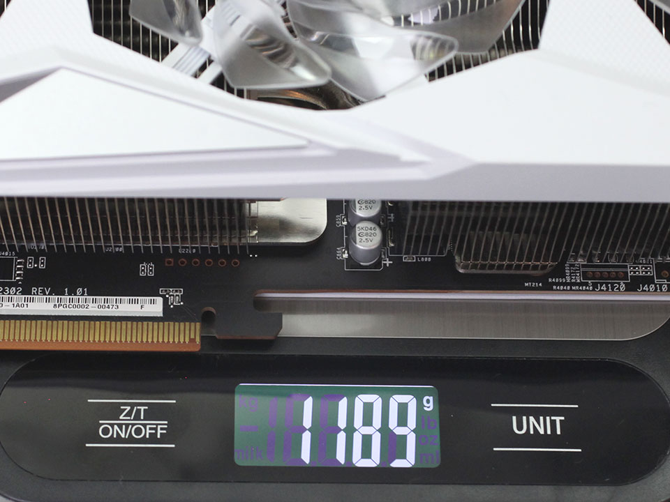
Dimensions of the card are 30.5 x 13.0 cm, and it weighs 1189 g.
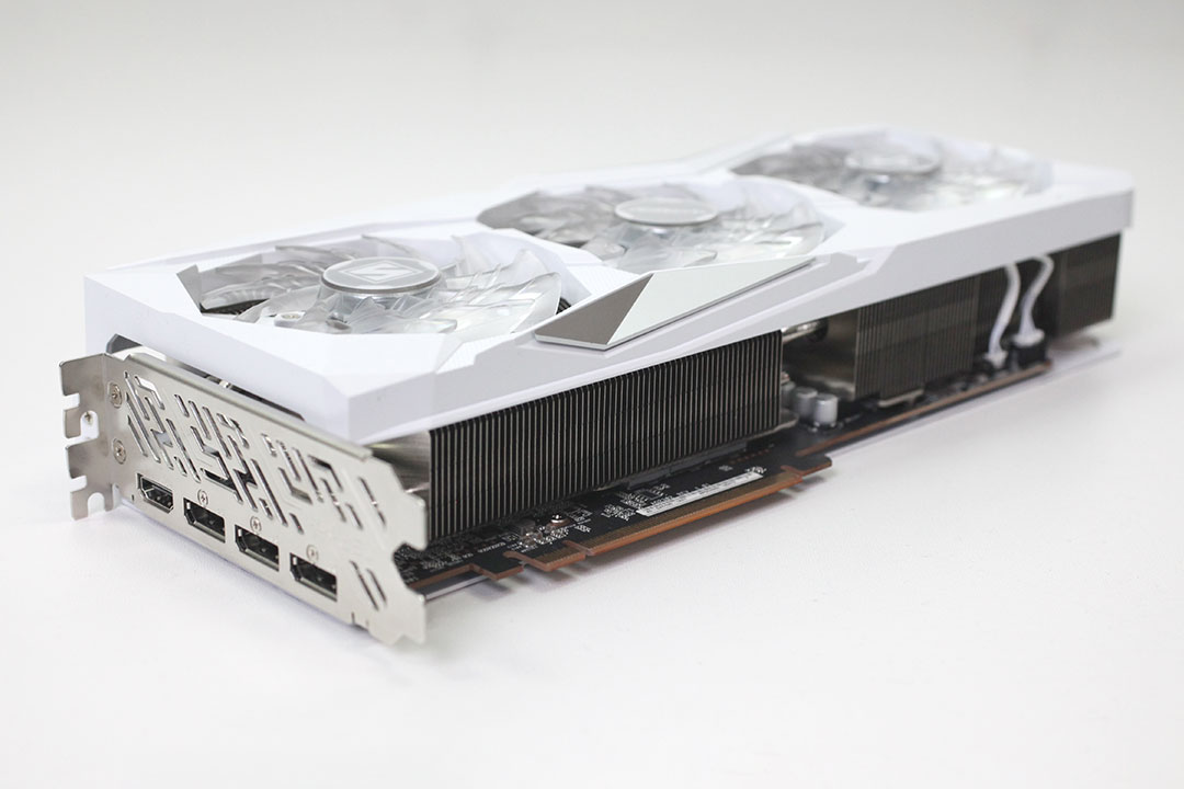
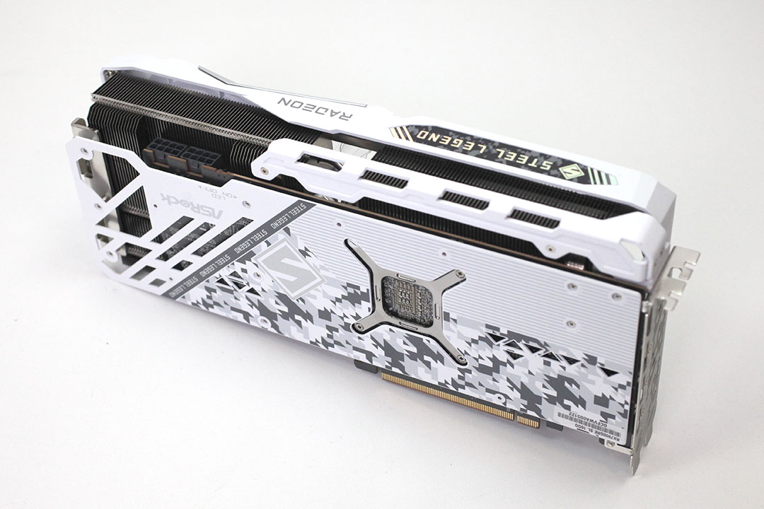
Installation requires three slots in your system.

Display connectivity includes three standard DisplayPort 2.1 ports (RDNA 2 had 1.4a) and one HDMI 2.1a (same as RDNA 2).
AMD has upgraded their encode/decode setup. It now comes with two independent hardware units that can encode and decode two streams of video in parallel, or one stream at double the FPS rate. There's support for VP9, H.264, H.265 and AV1 decode, and encoding is supported for H.264, H.265 and AV1.
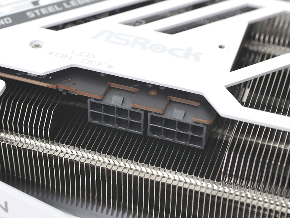
The card uses a classic dual 8-pin plus PCIe slot power input config, rated for 375 W maximum power. NVIDIA on the other hand uses the new 12+4 pin ATX 12V-2x6 connector, which is rated for up to 600 W of power draw.
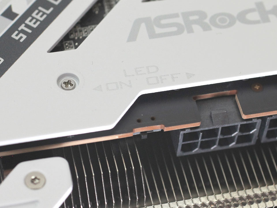
This switch lets you disable the card's lighting effects—no software required.
Our Patreon Silver Supporters can read articles in single-page format.
May 4th, 2025 10:16 EDT
change timezone
Latest GPU Drivers
New Forum Posts
- 12600KF high latency (18)
- The TPU UK Clubhouse (26186)
- Half Life 3 soon ? (0)
- Choosing an Internal HDD (57)
- Is RX 9070 VRAM temperature regular value or hotspot? (373)
- Windows 11 General Discussion (6011)
- Last game you purchased? (799)
- Are the 8 GB cards worth it? (817)
- Windows 12 (158)
- Have you got pie today? (16694)
Popular Reviews
- Clair Obscur: Expedition 33 Performance Benchmark Review - 33 GPUs Tested
- ASUS ROG Maximus Z890 Hero Review
- ASUS Radeon RX 9070 XT TUF OC Review
- Montech HS02 PRO Review
- NVIDIA GeForce RTX 5060 Ti 8 GB Review - So Many Compromises
- ASUS GeForce RTX 5090 Astral Liquid OC Review - The Most Expensive GPU I've Ever Tested
- Seasonic Vertex GX 850 W Review
- Upcoming Hardware Launches 2025 (Updated Apr 2025)
- ASRock Radeon RX 9070 XT Taichi OC Review - Excellent Cooling
- Team Group GC Pro 2 TB Review
Controversial News Posts
- AMD Radeon RX 9060 XT to Roll Out 8 GB GDDR6 Edition, Despite Rumors (129)
- NVIDIA Sends MSRP Numbers to Partners: GeForce RTX 5060 Ti 8 GB at $379, RTX 5060 Ti 16 GB at $429 (128)
- NVIDIA Launches GeForce RTX 5060 Series, Beginning with RTX 5060 Ti This Week (115)
- Nintendo Confirms That Switch 2 Joy-Cons Will Not Utilize Hall Effect Stick Technology (105)
- NVIDIA PhysX and Flow Made Fully Open-Source (95)
- Sony Increases the PS5 Pricing in EMEA and ANZ by Around 25 Percent (84)
- Parts of NVIDIA GeForce RTX 50 Series GPU PCB Reach Over 100°C: Report (78)
- Intel "Bartlett Lake-S" Gaming CPU is Possible, More Hints Appear for a 12 P-Core SKU (77)