 131
131
ASUS GeForce RTX 3090 STRIX OC Review
Test Setup »High-resolution PCB Pictures
These pictures are for the convenience of volt modders and people who would like to see all the finer details on the PCB. Feel free to link back to us and use these in your articles or forum posts.
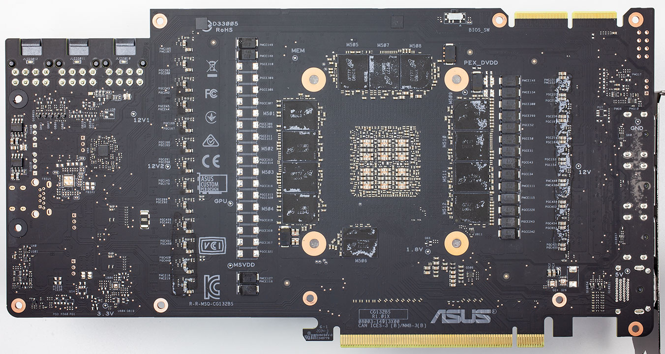
High-res versions are also available (front, back).
Circuit Board (PCB) Analysis


ASUS is using a pair of Monolithic Power Systems MP2888A 10-phase controllers to pull the GPU's various power domains.

Together, the vGPU is an 18-phase fare.

ASUS is using Texas Instruments NexFET CSD95481RWJ DrMOS chips. This is expensive stuff.

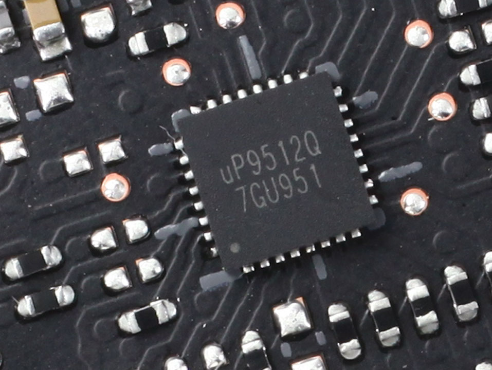

Memory voltage uses a 4-phase design and is generated by a UPI uP9512Q controller. Note the placement of the memory VRM phases—all spread out among the GPU power phases. The reason seems to be improved thermal performance and better voltage stability.

The GDDR6X memory chips are made by Micron and carry the model number D8BGX, which decodes to MT61K256M32JE-21. They are specified to run at 1313 MHz (21 Gbps GDDR6X effective).
GDDR6X doubles the data rate once again over GDDR6. It no longer transmits one bit of information by setting the voltage to either "on" or "off", but instead sends two bits of information at the same time by using four different voltage levels.

NVIDIA's GA102 graphics processor is the company's second Ampere architecture chip, the first one targeted at GeForce gamers. It is produced on a 8 nanometer process at Samsung and has a transistor count of 28 billion with a die size of 628 mm².
Jan 30th, 2025 13:34 EST
change timezone
Latest GPU Drivers
New Forum Posts
- NVIDIA RTX owners only - your opinion on DLSS Image quality (424)
- Connecting Arctic LFIII ARGB to motherboard (3)
- TechPowerUp Screenshot Thread (MASSIVE 56K WARNING) (4248)
- TPU's Rosetta Milestones and Daily Pie Thread (2168)
- RTX5090 GPU waterblocks, post your findings here. (21)
- Will you buy a RTX 5090? (257)
- Milestones (13973)
- Predator GM7000 Media Errors (0)
- Where to pin ARGB on motherboard (3)
- WCG Daily Numbers (12748)
Popular Reviews
- NVIDIA GeForce RTX 5080 Founders Edition Review
- NVIDIA DLSS 4 Transformer Review - Better Image Quality for Everyone
- ASUS GeForce RTX 5090 Astral OC Review - Astronomical Premium
- NVIDIA GeForce RTX 5090 Founders Edition Review - The New Flagship
- Galax GeForce RTX 5080 1-Click OC Review
- MSI GeForce RTX 5090 Suprim SOC Review
- MSI GeForce RTX 5090 Suprim Liquid SOC Review
- KLEVV URBANE V DDR5-7600 32 GB CL36 Review
- Palit GeForce RTX 5090 GameRock Review
- NVIDIA GeForce RTX 5090 PCI-Express Scaling
Controversial News Posts
- NVIDIA 2025 International CES Keynote: Liveblog (470)
- AMD Debuts Radeon RX 9070 XT and RX 9070 Powered by RDNA 4, and FSR 4 (349)
- AMD is Taking Time with Radeon RX 9000 to Optimize Software and FSR 4 (251)
- AMD Radeon RX 9070 XT & RX 9070 Custom Models In Stock at European Stores (226)
- AMD Denies Radeon RX 9070 XT $899 USD Starting Price Point Rumors (225)
- NVIDIA GeForce RTX 5090 Features 575 W TDP, RTX 5080 Carries 360 W TDP (217)
- New Leak Reveals NVIDIA RTX 5080 Is Slower Than RTX 4090 (212)
- AMD's Radeon RX 9070 Launch Faces Pricing Hurdles (175)