 72
72
ASUS GeForce RTX 4090 STRIX OC Review
(72 Comments) »Introduction
The new ASUS Republic of Gamers (ROG) Strix GeForce RTX 4090 OC represents the very best air-cooled custom-design implementation of the new NVIDIA flagship that ASUS has to offer, and we're reviewing it today. The ROG Strix brand was originally designed as a notch below bleeding-edge brands like the ROG Matrix and ROG Ares; but over the years has become one of the top custom-design graphics card brands to look out for, spanning all market segments. With the RTX 40-series, ASUS is dialing things up a bit, with an extremely premium product design that looks as much a work of art as technology; and has given it the company's highest factory-overclock for air-cooled graphics cards. In this review, we have the factory-overclocked "O24G" SKU of the RTX 4090 ROG Strix.

The NVIDIA GeForce RTX 4090 "Ada" is team-green's new-generation flagship product designed to achieve the "ends" of Moore's Law, if not through its "means." It promises a generational doubling in performance over what NVIDIA considered its previous flagship, the RTX 3080 (and not the RTX 3090/Ti); a nearly 50% improvement over the halo RTX 3090; while fitting into similar typical-power envelopes as the RTX 3090, at 450 W. In addition, Ada seeks to further reduce the frame-rate impact of enabling ray tracing, by improving its entire ray tracing hardware set; and introduces the new DLSS 3 feature with a breakthrough new AI-based complete frame-generation technique that creates unique new frames entirely using AI, without involving the bulk of the graphics rendering pipeline; thereby doubling the frame-rate.
The GeForce Ada graphics architecture heralds the 3rd generation of NVIDIA RTX real-time ray tracing technology, which blends conventional raster 3D graphics with real-time ray traced elements such as reflections, shadows, illumination, and motion-blur. With it, NVIDIA is debuting 3rd generation RT cores that come with two new hardware components accelerating ray tracing more accurately, unburdening the CUDA cores; and 4th generation Tensor cores, which leverage 8-bit and 4-bit math formats to increase AI inference performance by an order of magnitude over the previous-generation. The "Ada" CUDA cores feature shader-execution reordering capabilities, which improve shader-bound ray tracing workloads; and benefit from much higher clock-speeds.
The GeForce RTX 4090 is based on the new 5 nm "AD102" silicon, with a mammoth 76 billion transistors, crammed onto a die that's actually smaller than its predecessor. NVIDIA carved the RTX 4090 out of this silicon by enabling 16,384 CUDA cores from 128 SM (out of 18,432 CUDA cores across 144 SM). The card gets the same 24 GB of 21 Gbps GDDR6X memory across a 384-bit wide memory bus as the RTX 3090 Ti, which works out to the same 1008 GB/s bandwidth, but NVIDIA has significantly increased the on-die caches, now with an L2 cache of 72 MB (up from 6 MB on the RTX 3090).
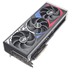
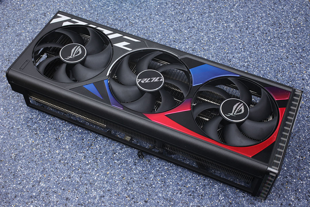
The ASUS ROG Strix RTX 4090 OC features a very cyberpunk-looking cooling solution that's the largest among the cards we have today. High-quality dual-tone metal elements elegantly fuse with addressable RGB LED diffusers, to create a slick-futuristic look. There are several generational innovations with the latest ROG STRIX, including the latest-generation Axial-Tech 0dB fans, a meaty multi fin-stack heatsink with a vapor-chamber plate; and plenty of gamer and enthusiast-relevant features that include additional case-fan headers, an ARGB header, and dual-BIOS. There's a nifty factory-overclocked GPU Boost speed of 2.61 GHz, compared to 2.52 GHz reference. All this comes at a stiff price-premium, with ASUS asking $2,000 for this card, a $400 or 25% premium over the $1,600 NVIDIA baseline price for the RTX 4090.
| Price | Cores | ROPs | Core Clock | Boost Clock | Memory Clock | GPU | Transistors | Memory | |
|---|---|---|---|---|---|---|---|---|---|
| RTX 2080 | $400 | 2944 | 64 | 1515 MHz | 1710 MHz | 1750 MHz | TU104 | 13600M | 8 GB, GDDR6, 256-bit |
| RTX 3060 Ti | $450 | 4864 | 80 | 1410 MHz | 1665 MHz | 1750 MHz | GA104 | 17400M | 8 GB, GDDR6, 256-bit |
| RX 6700 XT | $410 | 2560 | 64 | 2424 MHz | 2581 MHz | 2000 MHz | Navi 22 | 17200M | 12 GB, GDDR6, 192-bit |
| RX 6750 XT | $470 | 2560 | 64 | 2495 MHz | 2600 MHz | 2250 MHz | Navi 22 | 17200M | 12 GB, GDDR6, 192-bit |
| RTX 2080 Ti | $550 | 4352 | 88 | 1350 MHz | 1545 MHz | 1750 MHz | TU102 | 18600M | 11 GB, GDDR6, 352-bit |
| RTX 3070 | $530 | 5888 | 96 | 1500 MHz | 1725 MHz | 1750 MHz | GA104 | 17400M | 8 GB, GDDR6, 256-bit |
| RTX 3070 Ti | $600 | 6144 | 96 | 1575 MHz | 1770 MHz | 1188 MHz | GA104 | 17400M | 8 GB, GDDR6X, 256-bit |
| RX 6800 | $580 | 3840 | 96 | 1815 MHz | 2105 MHz | 2000 MHz | Navi 21 | 26800M | 16 GB, GDDR6, 256-bit |
| RX 6800 XT | $600 | 4608 | 128 | 2015 MHz | 2250 MHz | 2000 MHz | Navi 21 | 26800M | 16 GB, GDDR6, 256-bit |
| RTX 3080 | $660 | 8704 | 96 | 1440 MHz | 1710 MHz | 1188 MHz | GA102 | 28000M | 10 GB, GDDR6X, 320-bit |
| RTX 3080 Ti | $850 | 10240 | 112 | 1365 MHz | 1665 MHz | 1188 MHz | GA102 | 28000M | 12 GB, GDDR6X, 384-bit |
| RX 6900 XT | $680 | 5120 | 128 | 2015 MHz | 2250 MHz | 2000 MHz | Navi 21 | 26800M | 16 GB, GDDR6, 256-bit |
| RX 6950 XT | $950 | 5120 | 128 | 2100 MHz | 2310 MHz | 2250 MHz | Navi 21 | 26800M | 16 GB, GDDR6, 256-bit |
| RTX 3090 | $950 | 10496 | 112 | 1395 MHz | 1695 MHz | 1219 MHz | GA102 | 28000M | 24 GB, GDDR6X, 384-bit |
| RTX 3090 Ti | $1200 | 10752 | 112 | 1560 MHz | 1950 MHz | 1313 MHz | GA102 | 28000M | 24 GB, GDDR6X, 384-bit |
| RTX 4090 | $1600 | 16384 | 176 | 2235 MHz | 2520 MHz | 1313 MHz | AD102 | 76300M | 24 GB, GDDR6X, 384-bit |
| ASUS RTX 4090 STRIX OC | $2000 | 16384 | 176 | 2235 MHz | 2610 MHz | 1313 MHz | AD102 | 76300M | 24 GB, GDDR6X, 384-bit |
GeForce Ada Architecture
The Ada graphics architecture heralds the third generation of the NVIDIA RTX technology, an effort toward increasing the realism in game visuals by leveraging real-time ray tracing, without the enormous amount of compute power required to draw purely ray-traced 3D graphics. This is done by blending conventional raster graphics with ray traced elements such as reflections, lighting, and global illumination, to name a few. The 3rd generation of RTX heralds the new higher IPC "Ada" CUDA core, 3rd generation RT core, 4th generation Tensor core, and the new Optical Flow Processor, a component that plays a key role in generating new frames without involving the GPU's main graphics rendering pipeline.


The GeForce Ada graphics architecture driving the RTX 4090 leverages the TSMC 5 nm EUV foundry process to increase transistor counts to a mammoth 76.3 billion transistors, a nearly 3-fold increase over the previous-generation; while the die-size is actually smaller, at 608 mm², compared to 628 mm² of the previous-generation GA102. The GPU features a PCI-Express 4.0 x16 host interface, and a 384-bit wide GDDR6X memory bus, which on the RTX 4090 wires out to 24 GB of memory. The Optical Flow Accelerator (OFA) is an independent top-level component. The chip features two NVENC and one NVDEC units in the GeForce RTX 40-series; while future professional-visualization graphics cards will have all six each of the NVENC and NVDEC components enabled.
The essential component hierarchy is similar to past generations of NVIDIA GPUs. The AD102 silicon features a whopping 12 Graphics Processing Clusters (GPCs), each of these has all the SIMD and graphics rendering machinery, and is a small GPU in its own right. Each GPC shares a raster engine (geometry processing components) and two ROP partitions (each with eight ROP units). The GPC of the AD102 contains six Texture Processing Clusters (TPCs), the main number-crunching machinery. Each of these has two Streaming Multiprocessors (SM), and a Polymorph unit. Each SM contains 128 CUDA cores across four partitions. Half of these CUDA cores are pure-FP32; while the other half is capable of FP32 or INT32. The SM retains concurrent FP32+INT32 math processing capability. The SM also contains a 3rd generation RT core, four 4th generation Tensor cores, some cache memory, and four TMUs. There are 12 SM per GPC, so 1,536 CUDA cores, 48 Tensor cores, and 12 RT cores; per GPC. Twelve GPCs hence add up to 18,432 CUDA cores, 576 Tensor cores, and 144 RT cores. Each GPC contributes 16 ROPs, so there are a mammoth 192 ROPs on the silicon. A 96 MB L2 cache serves as town-square for the various GPCs, memory controllers, and the PCIe host interface, to exchange data. NVIDIA carved the RTX 4090 out of the AD102 by disabling one of the twelve GPCs, and a further two TPCs from two of the other GPCs, as shown in the red-shaded parts of the block diagram above. The RTX 4090 has 72 MB L2 cache enabled (out of 96 MB physically present on the silicon).


The 3rd generation RT core accelerates the most math-intensive aspects of real-time ray tracing, including BVH traversal. Displaced micro-mesh engine is a revolutionary feature introduced with the new 3rd generation RT core, which accelerates the displaced micro-mesh feature. Just as mesh shaders and tessellation have had a profound impact on improving performance with complex raster geometry, allowing game developers to significantly increase geometric complexity; DMMs is a method to reduce the complexity of the bounding-volume hierarchy (BVH) data-structure, which is used to determine where a ray hits geometry. Previously the BVH had to capture even the smallest details to properly determine the intersection point. Ada's ray tracing architecture receives a major performance uplift from Shader Execution Reordering (SER), a software-defined feature that requires awareness from game-engines, to help the GPU reorganize and optimize worker threads associated with ray tracing.


The BVH now needn't have data for every single triangle on an object, but can represent objects with complex geometry as a coarse mesh of base triangles, which greatly simplifies the BVH data structure. A simpler BVH means less memory consumed and helps to greatly reduce ray tracing CPU load, because the CPU only has to generate a smaller structure. With older "Ampere" and "Turing" RT cores, each triangle on an object had to be sampled at high overhead, so the RT core could precisely calculate ray intersection for each triangle. With Ada, the simpler BVH, plus the displacement maps can be sent to the RT core, which is now able to figure out the exact hit point on its own. NVIDIA has seen 11:1 to 28:1 compression in total triangle counts. This reduces BVH compile times by 7.6x to over 15x, in comparison to the older RT core; and reducing its storage footprint by anywhere between 6.5 to 20 times. DMMs could reduce disk- and memory bandwidth utilization, utilization of the PCIe bus, as well as reduce CPU utilization. NVIDIA worked with Simplygon and Adobe to add DMM support for their tool chains.


Opacity Micro Meshes (OMM) is a new feature introduced with Ada to improve rasterization performance, particularly with objects that have alpha (transparency data). Most low-priority objects in a 3D scene, such as leaves on a tree, are essentially rectangles with textures on the leaves where the transparency (alpha) creates the shape of the leaf. RT cores have a hard time intersecting rays with such objects, because they're not really in the shape that they appear (they're really just rectangles with textures that give you the illusion of shape). Previous-generation RT cores had to have multiple interactions with the rendering stage to figure out the shape of a transparent object, because they couldn't test for alpha by themselves.


This has been solved by using OMMs. Just as DMMs simplify geometry by creating meshes of micro-triangles; OMMs create meshes of rectangular textures that align with parts of the texture that aren't alpha, so the RT core has a better understanding of the geometry of the object, and can correctly calculate ray intersections. This has a significant performance impact on shading performance in non-RT applications, too. Practical applications of OMMs aren't just low-priority objects such as vegetation, but also smoke-sprites and localized fog. Traditionally there was a lot of overdraw for such effects, because they layered multiple textures on top of each other, that all had to be fully processed by the shaders. Now only the non-opaque pixels get executed—OMMs provide a 30 percent speedup with graphics buffer fill-rates, and a 10 percent impact on frame-rates.
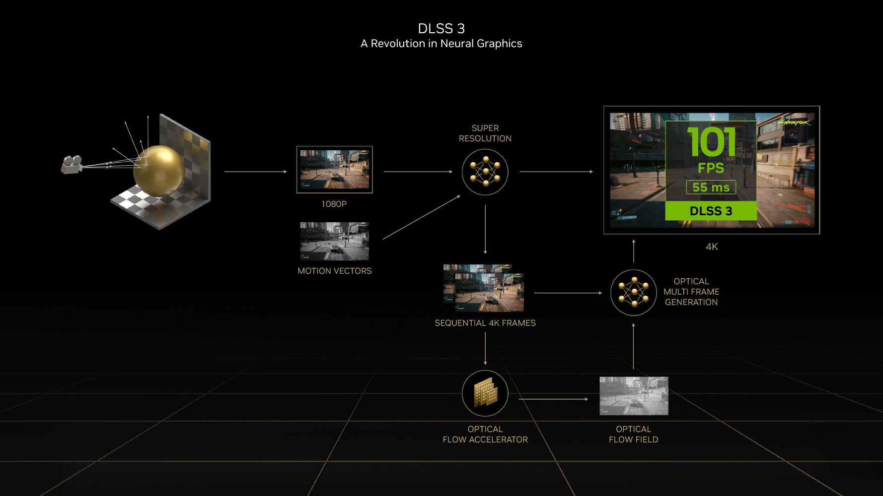

DLSS 3 introduces a revolutionary new feature that promises a doubling in frame-rate at comparable quality, it's called AI frame-generation. While it has all the features of DLSS 2 and its AI super-resolution (scaling up a lower-resolution frame to native resolution with minimal quality loss); DLSS 3 can generate entire frames simply using AI, without involving the graphics rendering pipeline.


Every alternating frame with DLSS 3 is hence AI-generated, without being a replica of the previous rendered frame. This is possible only on the Ada graphics architecture, because of a hardware component called the optical flow accelerator (OFA), which assists in predicting what the next frame could look like, by creating what NVIDIA calls an optical flow-field. OFA ensures that the DLSS 3 algorithm isn't confused by static objects in a rapidly-changing 3D scene (such as a race sim). The process heavily relies on the performance uplift introduced by the FP8 math format of the 4th generation Tensor core. A third key ingredient of DLSS 3 is Reflex. By reducing the rendering queue to zero, Reflex plays a vital role in ensuring that frame-times with DLSS 3 are at an acceptable level, and a render-queue doesn't confuse the upscaler. A combination of OFA and the 4th Gen Tensor core is why the Ada architecture is required to use DLSS 3, and why it won't work on older architectures.
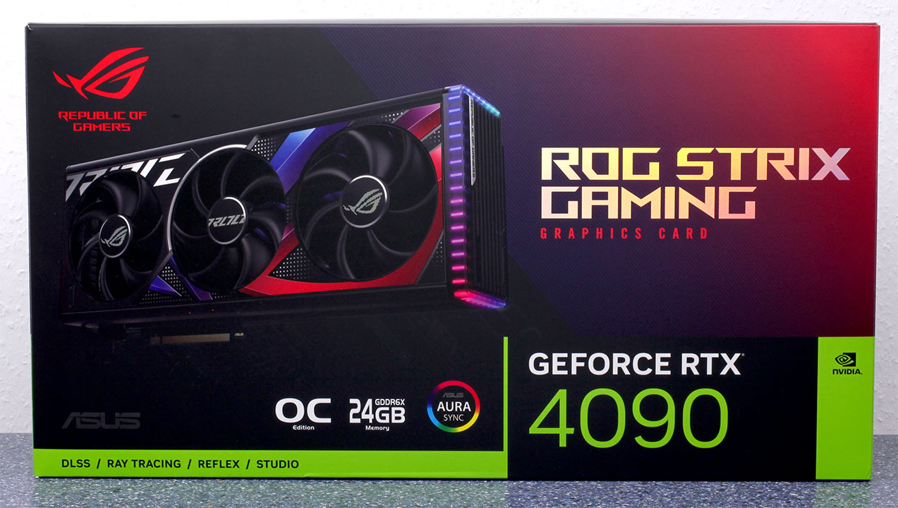
Packaging

The Card


ASUS created an amazing new look for their GeForce 40 Series graphics card. Both the main cooler shroud and the backplate are made of thick metal. While the color theme on the backplate is black with silvery highlights, the front introduces gradients of blue and red that look mighty good. The colors change subtly as you adjust your viewing angle of the card.
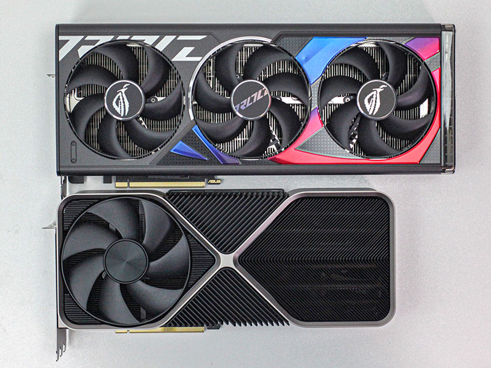

The STRIX is much bigger than the NVIDIA Founders Edition.


Dimensions of the card are 36.0 x 15.0 cm, and it weighs 2504 g. The height is hard to see on the photo, refer to the RTX 4080 STRIX review where I've shot from a better angle, the 150 mm height is easier to recognize there.


Installation requires four slots in your system.

Display connectivity includes three standard DisplayPort 1.4a ports and two HDMI 2.1a (same technology as Ampere).
NVIDIA introduced the concept of dual NVDEC and NVENC Codecs with the Ada architecture. This means there are two independent sets of hardware-accelerators; so you can encode and decode two streams of video in parallel or one stream at double the FPS rate. The new 8th Gen NVENC now accelerates AV1 encoding, besides HEVC. You also get an "optical flow accelerator" unit that is able to calculate intermediate frames for videos, to smooth playback. The same hardware unit is used for frame generation in DLSS 3.


The card uses the new 12+4 pin ATX 12VHPWR connector, which is rated for up to 600 W of power draw. An adapter cable from 4x PCIe 8-pin is included, you can also run the card with just three 8-pins.

This BIOS switch lets you toggle from the default performance BIOS to the quiet BIOS which runs a more relaxed fan curve.

Near the back of the card you'll find two fan headers that run the connected fans at the same speed as the GPU fans, including fan stop. This makes it a great option to control the case fans according to graphics card temperature.
Teardown

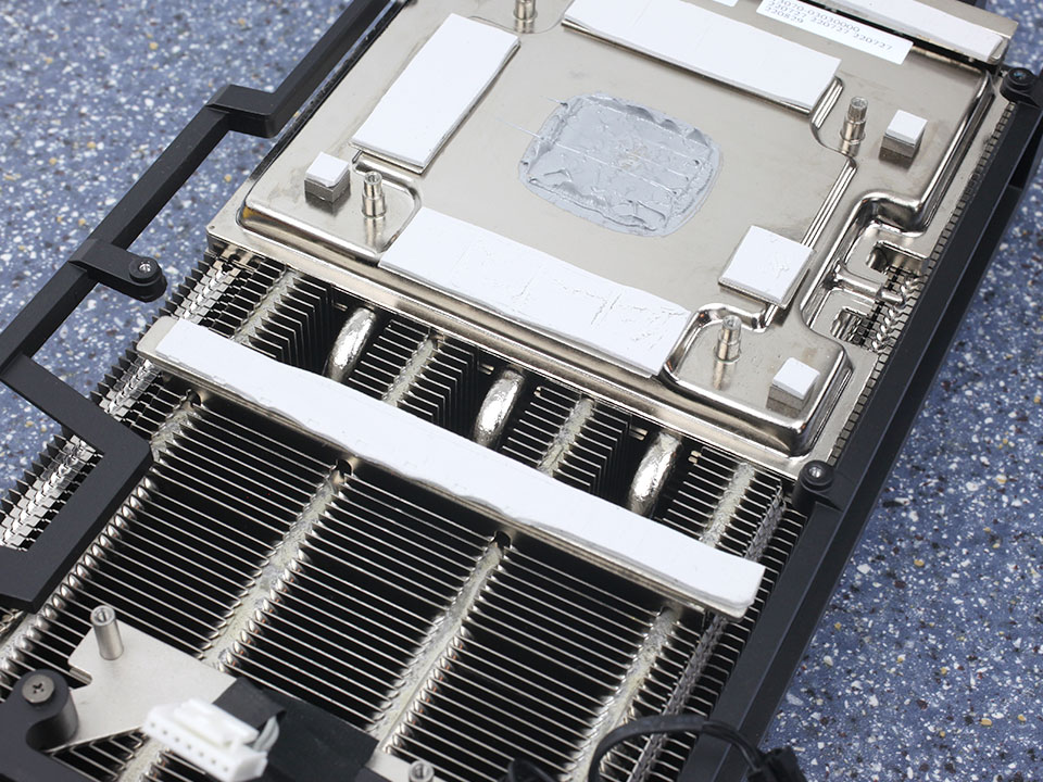
The ASUS thermal solution is massive, it uses a vapor-chamber base to soak up heat from the GPU quickly, and seven heatpipes are connected to the heatsink. The main heatsink also provides cooling for the VRM and memory chips.
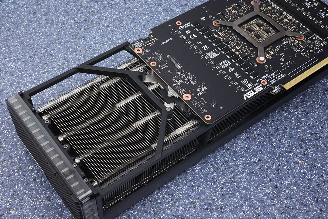
Once the backplate is removed you can see how the PCB is shorter to leave some room for air to flow through the card.

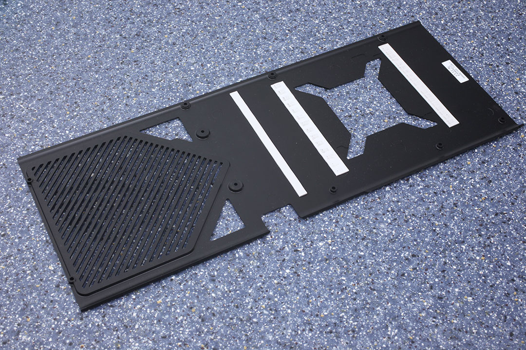
The backplate is made of thick metal and protects the card against damage during installation and handling.
High-resolution PCB Pictures
These pictures are for the convenience of volt modders and people who would like to see all the finer details on the PCB. Feel free to link back to us and use these in your articles, videos or forum posts.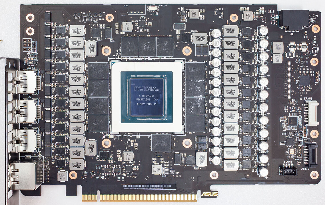
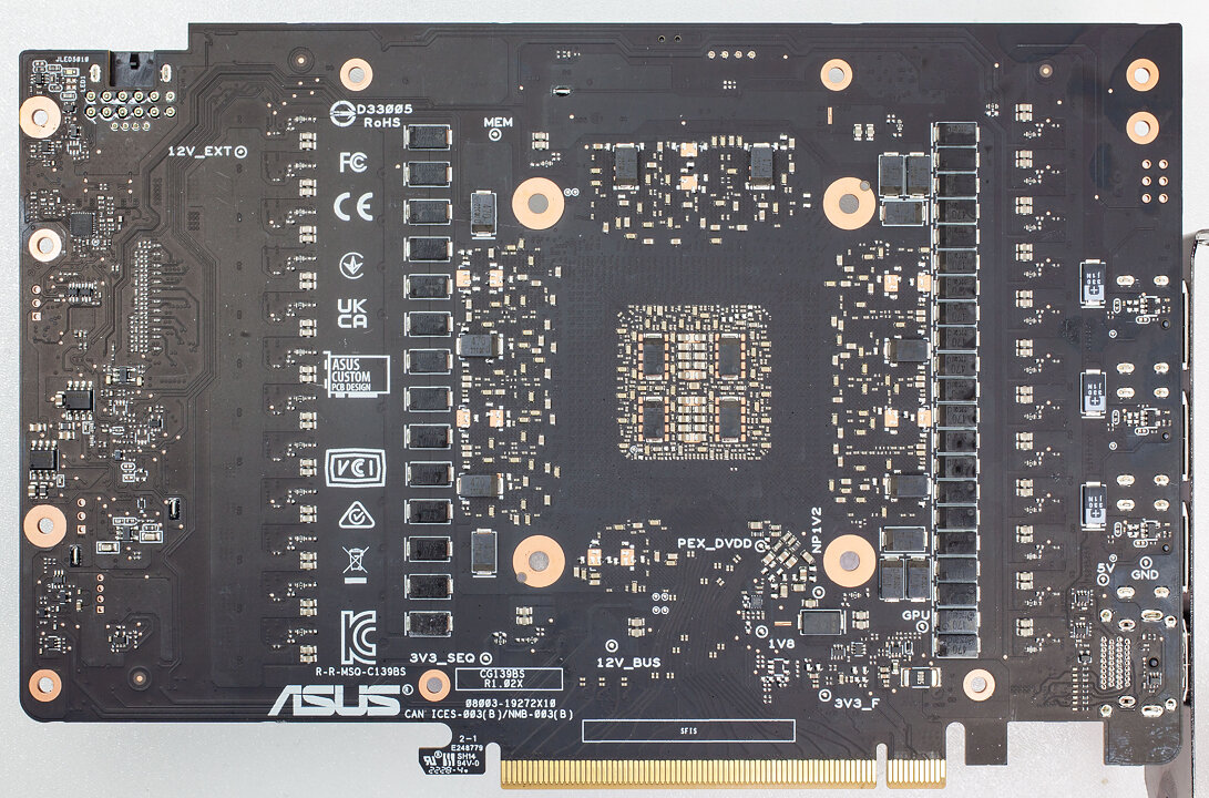
High-resolution versions are also available (front, back).
Our Patreon Silver Supporters can read articles in single-page format.
May 6th, 2025 00:43 EDT
change timezone
Latest GPU Drivers
New Forum Posts
- Pc crash (6)
- is it possible to buy a sata to propietary dell pata adapter? (12)
- Graphics card..Need help. New to pc. 3070 (48)
- Steam installer asked me if I got Dial Up! (10)
- Request for advice [Big Build] (61)
- 9070XT Nitro vs Taichi? (15)
- The TPU UK Clubhouse (26200)
- RX 9070 availability (275)
- laptop cooler- more smaller fans or less larger fans? (0)
- Why doesn't every house have solar installed? (332)
Popular Reviews
- Arctic Liquid Freezer III Pro 360 A-RGB Review
- ASUS Radeon RX 9070 XT TUF OC Review
- Clair Obscur: Expedition 33 Performance Benchmark Review - 33 GPUs Tested
- ASUS ROG Maximus Z890 Hero Review
- Zotac GeForce RTX 5070 Ti Amp Extreme Review
- Upcoming Hardware Launches 2025 (Updated Apr 2025)
- Seasonic Vertex GX 850 W Review
- Sapphire Radeon RX 9070 XT Nitro+ Review - Beating NVIDIA
- ASUS GeForce RTX 5090 Astral Liquid OC Review - The Most Expensive GPU I've Ever Tested
- Montech HS02 PRO Review
Controversial News Posts
- AMD Radeon RX 9060 XT to Roll Out 8 GB GDDR6 Edition, Despite Rumors (131)
- NVIDIA Sends MSRP Numbers to Partners: GeForce RTX 5060 Ti 8 GB at $379, RTX 5060 Ti 16 GB at $429 (128)
- NVIDIA Launches GeForce RTX 5060 Series, Beginning with RTX 5060 Ti This Week (115)
- Nintendo Confirms That Switch 2 Joy-Cons Will Not Utilize Hall Effect Stick Technology (105)
- NVIDIA PhysX and Flow Made Fully Open-Source (95)
- Sony Increases the PS5 Pricing in EMEA and ANZ by Around 25 Percent (84)
- Parts of NVIDIA GeForce RTX 50 Series GPU PCB Reach Over 100°C: Report (78)
- Intel "Bartlett Lake-S" Gaming CPU is Possible, More Hints Appear for a 12 P-Core SKU (77)