 78
78
ASUS Radeon RX 7900 GRE TUF OC Review
(78 Comments) »Introduction
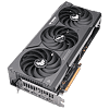
ASUS TUF Gaming Radeon RX 7900 GRE OC is the company's most premium custom-design graphics card based on AMD's latest performance segment offering. While we await ASUS's coveted ROG Strix brand to extend to the Radeon RX 7900 and RX 7800 series, the TUF Gaming brand currently represents ASUS's very best, and interestingly, it can still measure up to the best custom-design Radeon RX 7000 series cards out there. TUF Gaming, over the years, has evolved into an impressive custom-design brand from ASUS, which covers all the basics while also featuring high-end noise optimization, and overclocking features. While the card does include some basic ARGB lighting, it's not as much as you get on an ROG Strix product. If max RGB is your thing, then ASRock, Sapphire, or PowerColor have some jaw-dropping custom designs for you.
The AMD Radeon RX 7900 GRE isn't all that new—it was launched in mid-2023 as a China-exclusive limited edition SKU commemorating the Chinese year of the rabbit, hence the name Golden Rabbit Edition (GRE). This product is designed to fit between the RX 7900 XT and the RX 7800 XT in terms of performance, but with costs closer to the latter. AMD found itself disrupted in January 2024, when NVIDIA refreshed the higher end of its RTX 40-series with cards such as the RTX 4070 Super, which restored NVIDIA's competitiveness under the $600-mark, where the RX 7800 XT challenged the RTX 4070. AMD responded by simply giving the RX 7900 GRE a worldwide launch.

The Radeon RX 7900 GRE has an interesting product development story. The RX 7800 XT maxes out the Navi 32 silicon, and the only way AMD could create the RX 7900 GRE was by tapping into the larger Navi 31 silicon, and making its board partners use PCBs from the RX 7900 series—suboptimal when trying to compete in the $500-range. The company had developed a compacted version of the Navi 31, which it intended to use for mobile Radeon RX 7900 series SKUs. This is basically the Navi 31 chiplet GPU, but placed on a package that's exactly the size of the Navi 32, with a similar pin-map, and wiring for a 256-bit wide memory bus. AMD used this compact Navi 31 variant, and made its partners reuse PCBs and cooling solutions from their RX 7800 XT products, to create the RX 7900 GRE. Both SKUs have similar power limits, and so reusing the PCBs and coolers became easy.
The Radeon RX 7900 GRE is carved out of Navi 31 by enabling 80 out of the 96 RDNA 3 compute units present on the 5 nm GCD. This works out to 5,120 stream processors, 160 AI accelerators, 80 Ray accelerators, and 320 TMUs. 160 out of the 192 ROPs present are enabled. The chip has just four of the six memory cache dies (MCDs) enabled, each with a 16 MB segment of the Infinity Cache, and a 64-bit portion of the memory bus. It hence has 64 MB of Infinity Cache, and a 256-bit memory bus. What's interesting here is that AMD chose a lower memory speed for the RX 7900 GRE compared to the RX 7800 XT—18 Gbps vs. 19.5 Gbps. Perhaps every effort was made to bring the two SKUs to an identical power profile.
Powering the Radeon RX 7900 GRE is the AMD RDNA 3 graphics architecture, which introduces generational performance increases by leveraging the 5 nm process, at least where it matters. The new dual-issue rate compute unit offers an over 17% IPC increase over the RDNA 2 compute unit. The new AI accelerator is a component that prepares matrix math for further execution on the stream processors, greatly accelerating AI workloads; while the new 2nd generation Ray accelerator features a 50% performance improvement. AMD also introduced the multi-draw indirect accelerator (MDIA), a component that vastly speeds up Direct3D 12 workloads that use the multi-draw indirect instruction.
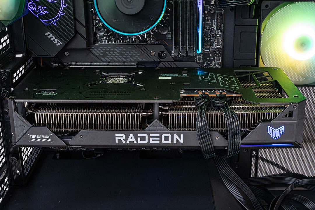
The ASUS TUF Gaming RX 7900 GRE features a similar cooling solution and PCB to the company's RX 7800 XT, for the reasons we explained above. This is a highly capable package, and ASUS has given the card a formidable fin-stack based cooling solution that uses its latest Axial-Tech fans. The metal cooler shroud gives it an industrial look, and is very airy for the heatsink underneath. There is minimal use of RGB, in the form of a single light strip. The card offers features such as dual-BIOS, and factory overclocked speeds of 1972 MHz Game Clocks (compared to 1880 MHz reference), while leaving the memory untouched at 18 Gbps. ASUS is pricing this card at $600, a reasonable $50 premium over the AMD baseline, but a price that puts it on par with the GeForce RTX 4070 Super.
Short 10-Minute Video Summary Comparing 6x RX 7900 GRE
Our goal with the videos is to create short summaries, not go into all the details and test results, which can be found in this written review.
| Price | Cores | ROPs | Core Clock | Boost Clock | Memory Clock | GPU | Transistors | Memory | |
|---|---|---|---|---|---|---|---|---|---|
| RTX 3070 | $310 | 5888 | 96 | 1500 MHz | 1725 MHz | 1750 MHz | GA104 | 17400M | 8 GB, GDDR6, 256-bit |
| RTX 3070 Ti | $350 | 6144 | 96 | 1575 MHz | 1770 MHz | 1188 MHz | GA104 | 17400M | 8 GB, GDDR6X, 256-bit |
| RX 6800 | $450 | 3840 | 96 | 1815 MHz | 2105 MHz | 2000 MHz | Navi 21 | 26800M | 16 GB, GDDR6, 256-bit |
| RX 7700 XT | $430 | 3456 | 96 | 2171 MHz | 2544 MHz | 2250 MHz | Navi 32 | 26500M | 12 GB, GDDR6, 192-bit |
| RX 6800 XT | $500 | 4608 | 128 | 2015 MHz | 2250 MHz | 2000 MHz | Navi 21 | 26800M | 16 GB, GDDR6, 256-bit |
| RTX 3080 | $450 | 8704 | 96 | 1440 MHz | 1710 MHz | 1188 MHz | GA102 | 28000M | 10 GB, GDDR6X, 320-bit |
| RTX 4070 | $525 | 5888 | 64 | 1920 MHz | 2475 MHz | 1313 MHz | AD104 | 35800M | 12 GB, GDDR6X, 192-bit |
| RX 7800 XT | $500 | 3840 | 96 | 2124 MHz | 2430 MHz | 2425 MHz | Navi 32 | 28100M | 16 GB, GDDR6, 256-bit |
| RX 6900 XT | $650 | 5120 | 128 | 2015 MHz | 2250 MHz | 2000 MHz | Navi 21 | 26800M | 16 GB, GDDR6, 256-bit |
| RX 6950 XT | $630 | 5120 | 128 | 2100 MHz | 2310 MHz | 2250 MHz | Navi 21 | 26800M | 16 GB, GDDR6, 256-bit |
| RTX 3090 | $800 | 10496 | 112 | 1395 MHz | 1695 MHz | 1219 MHz | GA102 | 28000M | 24 GB, GDDR6X, 384-bit |
| RTX 4070 Super | $590 | 7168 | 80 | 1980 MHz | 2475 MHz | 1313 MHz | AD104 | 35800M | 12 GB, GDDR6X, 192-bit |
| RX 7900 GRE | $550 | 5120 | 160 | 1880 MHz | 2245 MHz | 2250 MHz | Navi 31 | 57700M | 16 GB, GDDR6, 256-bit |
| ASUS RX 7900 GRE TUF OC | $600 | 5120 | 160 | 1972 MHz | 2333 MHz | 2250 MHz | Navi 31 | 57700M | 16 GB, GDDR6, 256-bit |
| RTX 4070 Ti | $720 | 7680 | 80 | 2310 MHz | 2610 MHz | 1313 MHz | AD104 | 35800M | 12 GB, GDDR6X, 192-bit |
| RTX 4070 Ti Super | $800 | 8448 | 96 | 2340 MHz | 2610 MHz | 1313 MHz | AD103 | 45900M | 16 GB, GDDR6X, 256-bit |
| RX 7900 XT | $700 | 5376 | 192 | 2000 MHz | 2400 MHz | 2500 MHz | Navi 31 | 57700M | 20 GB, GDDR6, 320-bit |
| RTX 3090 Ti | $1050 | 10752 | 112 | 1560 MHz | 1950 MHz | 1313 MHz | GA102 | 28000M | 24 GB, GDDR6X, 384-bit |
| RTX 4080 | $1200 | 9728 | 112 | 2205 MHz | 2505 MHz | 1400 MHz | AD103 | 45900M | 16 GB, GDDR6X, 256-bit |
| RTX 4080 Super | $1300 | 10240 | 112 | 2295 MHz | 2550 MHz | 1438 MHz | AD103 | 45900M | 16 GB, GDDR6X, 256-bit |
| RX 7900 XTX | $910 | 6144 | 192 | 2300 MHz | 2500 MHz | 2500 MHz | Navi 31 | 57700M | 24 GB, GDDR6, 384-bit |
| RTX 4090 | $1850 | 16384 | 176 | 2235 MHz | 2520 MHz | 1313 MHz | AD102 | 76300M | 24 GB, GDDR6X, 384-bit |
Packaging


The Card


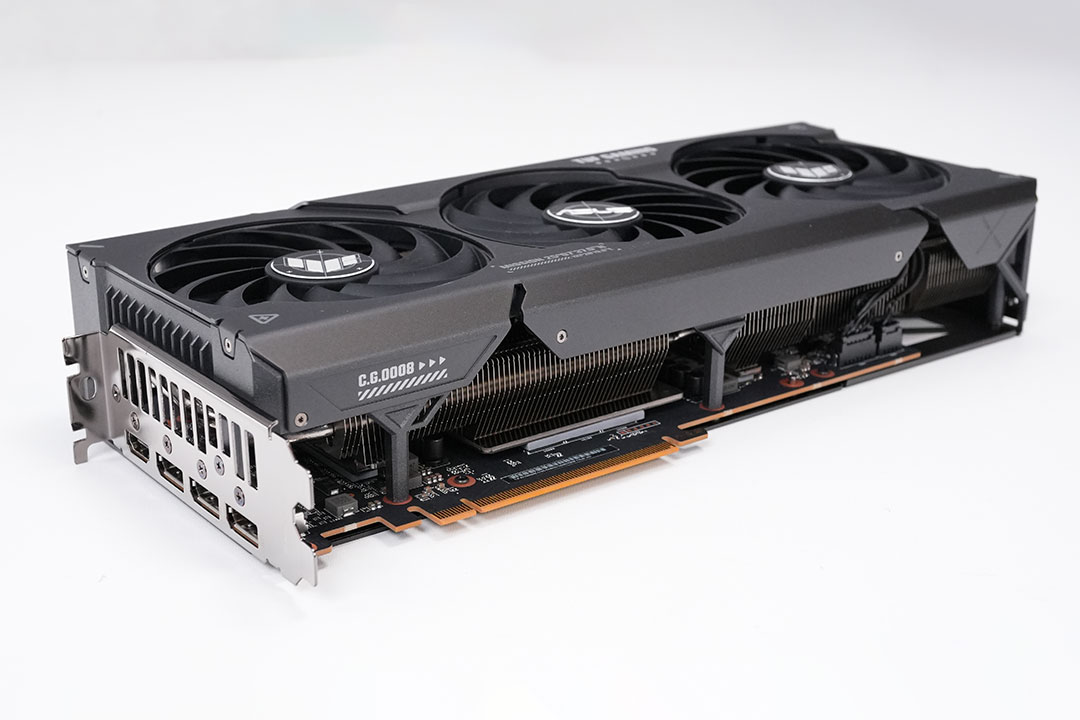
The ASUS RX 7900 GRE TUF OC is instantly recognizable, thanks to its bulky look that's a feature of the TUF series. On the other side you'll find a metal backplate that has a cutout for air to flow through.
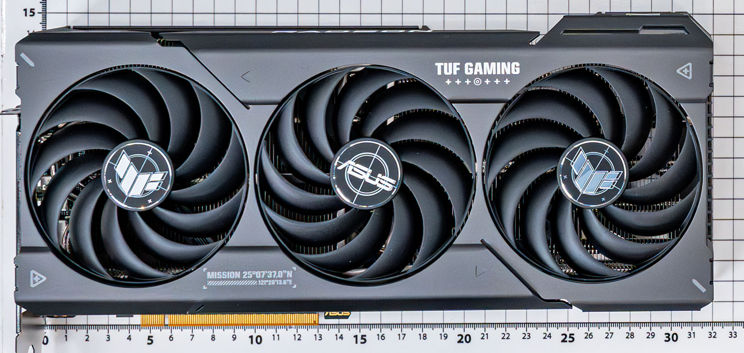

Dimensions of the card are 32.0 x 15.0 cm, and it weighs 1326 g.

Installation requires three slots in your system. We measured the card's width to be 60 mm.
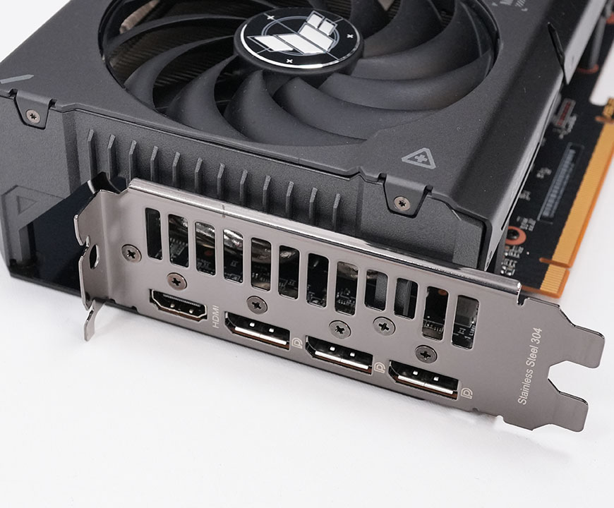
Display connectivity includes three standard DisplayPort 2.1 ports (RDNA 2 had 1.4a) and one HDMI 2.1a (same as RDNA 2).
AMD has upgraded their encode/decode setup. It now comes with two independent hardware units that can encode and decode two streams of video in parallel, or one stream at double the FPS rate. There's support for VP9, H.264, H.265 and AV1 decode, and encoding is supported for H.264, H.265 and AV1.

The card uses a classic dual 8-pin plus PCIe slot power input config, rated for 375 W maximum power. NVIDIA on the other hand uses the new 12+4 pin ATX 12V-2x6 connector, which is rated for up to 600 W of power draw.


The card comes with adjustable lighting on the corner near the power connectors.
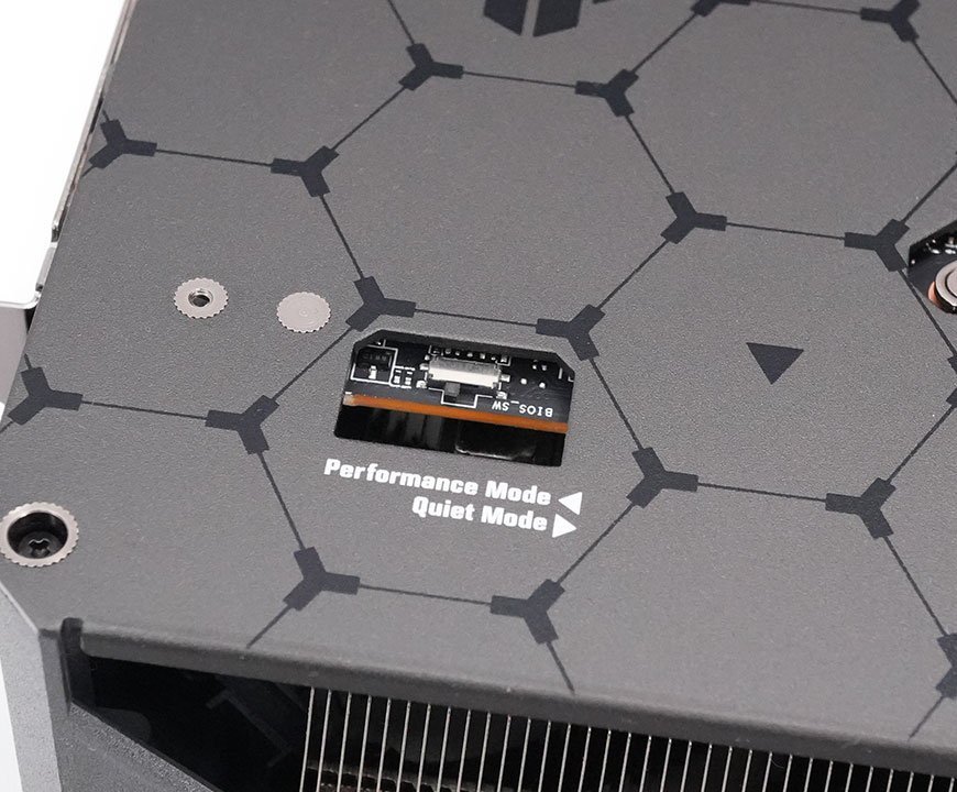
The dual BIOS switch lets you switch to a secondary "quiet" BIOS, which runs at a more relaxed fan curve.
Teardown


ASUS lets you remove the main cooler shroud, so the fans can be cleaned and replaced easily, without disturbing the thermal paste on the main cooler.

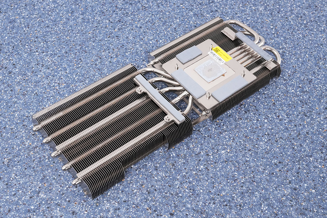

The thermal solution on the ASUS TUF OC has five heatpipes. The main heatsink also provides cooling for the memory chips and VRM circuitry.
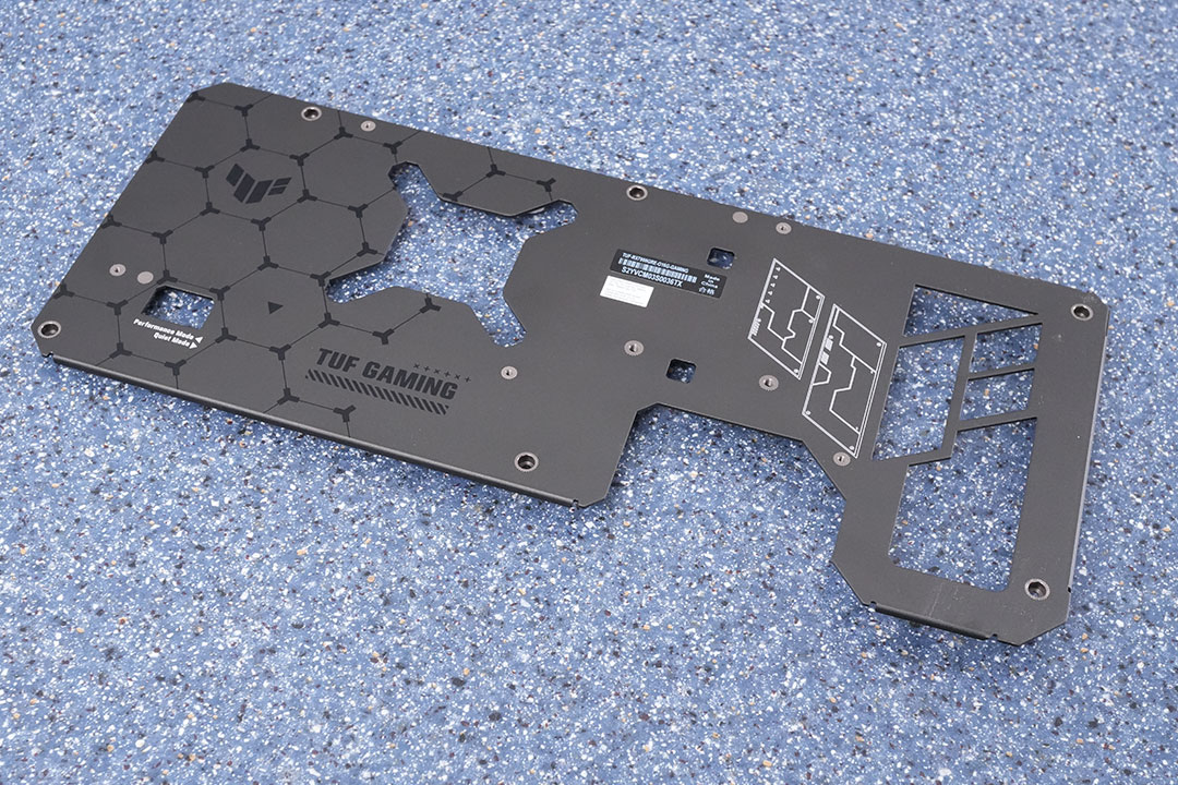

The backplate is made of metal and protects the card against damage during installation and handling.
High-resolution PCB Pictures
These pictures are for the convenience of volt modders and people who would like to see all the finer details on the PCB. Feel free to link back to us and use these in your articles, videos or forum posts.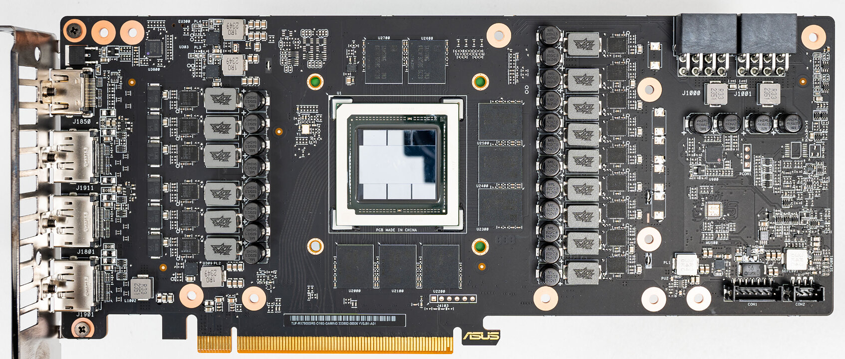

High-resolution versions are also available (front, back).
Circuit Board (PCB) Analysis
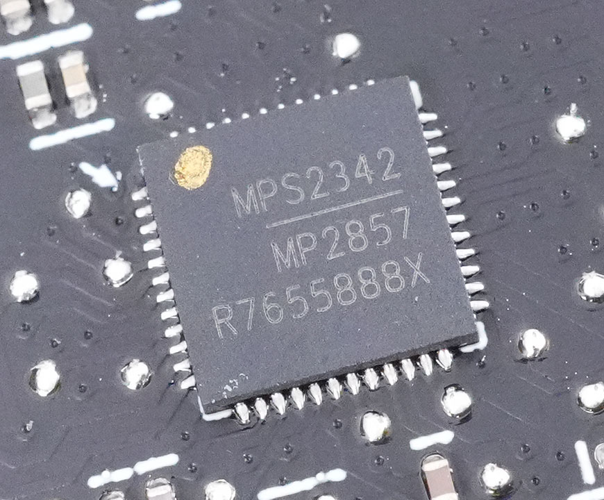
GPU voltage is a 12-phase design, managed by a Monolithic Power Systems MP2857 controller.

Monolithic MP87997 DrMOS components are used for GPU voltage; they are rated for 70 A of current each.
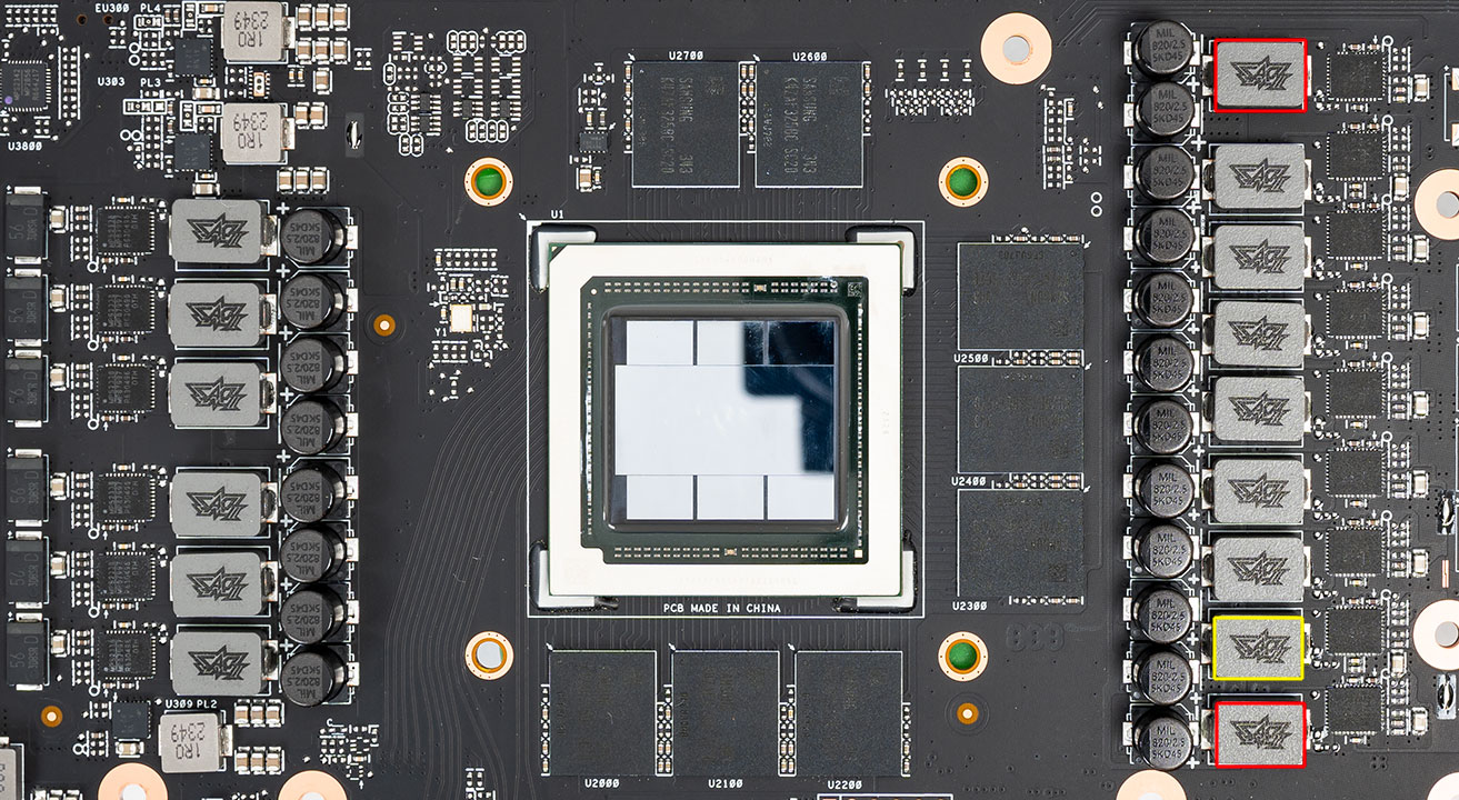

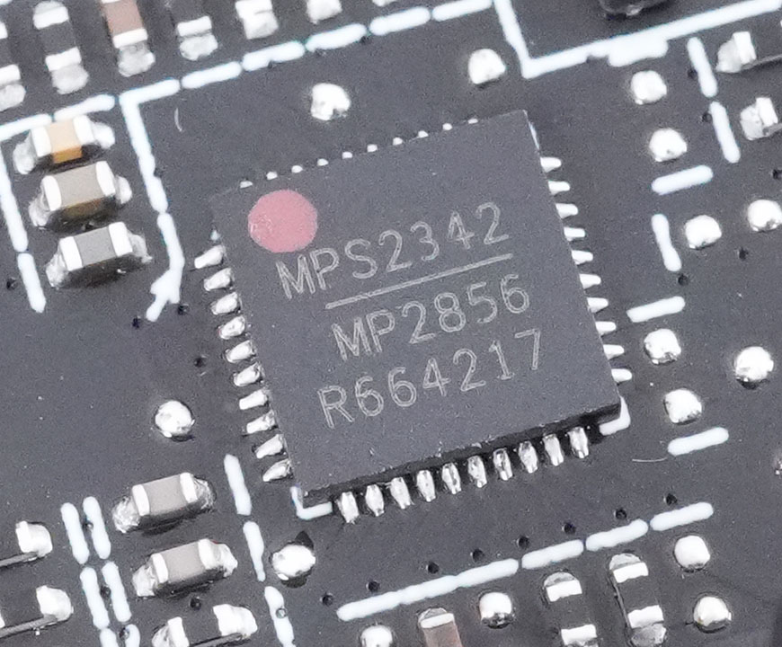
Memory voltage is a 2+1-phase design, managed by two Monolithic Power Systems MP2856 controllers.
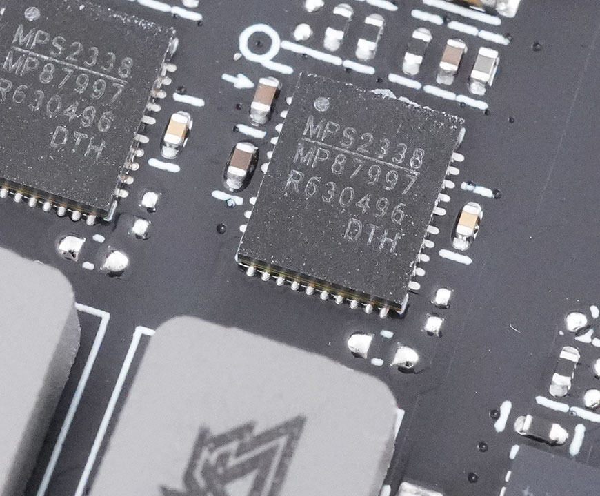
For memory, Monolithic MP87997 DrMOS with a 70 A rating are used here, too.
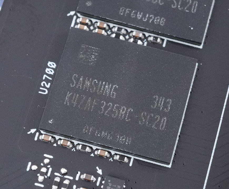
The GDDR6 memory chips are made by Samsung and carry the model number K4ZAF325BC-SC20. They are specified to run at 2500 MHz (20 Gbps effective).
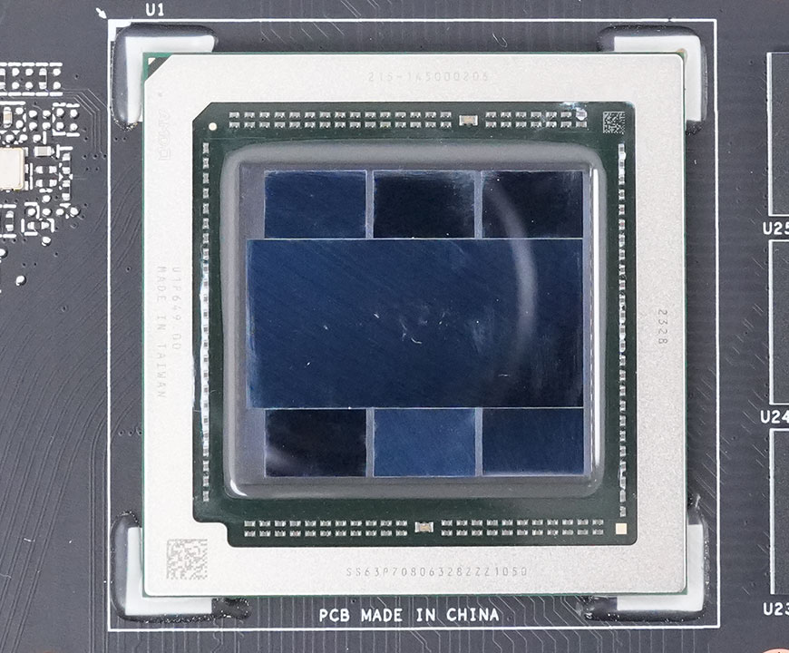
The GPU chip on the Radeon RX 7900 GRE is Navi 31, but it looks quite different to the chips on the RX 7900 XT and XTX. The physical size of the package is reduced, due to its roots in the mobile space. You still get the full-size GCD (graphics compute die) in the center, surrounded by four MCD (memory cache dies). The other two MCDs that you see pictured are non-functional dummies that are used to ensure structural stability of the chip, when a cooler is pushing down on it. While they look similar, the MCDs are not HBM chips. The MCDs are fabricated on a 6 nm process at TSMC Taiwan with a die size of 36.6 mm² each, the GCD is fabricated using TSMC's 5 nanometer node, with a die size of 300 mm². The combined transistor count of the GPU is 57.7 billion.
Our Patreon Silver Supporters can read articles in single-page format.
May 5th, 2025 12:59 EDT
change timezone
Latest GPU Drivers
New Forum Posts
- RX 9000 series GPU Owners Club (652)
- Windows 12 (178)
- Are the 8 GB cards worth it? (872)
- A Question for RTX 4070 Ti Super ROPs (3)
- What phone you use as your daily driver? And, a discussion of them. (1674)
- Post Your TIMESPY, PCMARK10 & FIRESTRIKE SCORES! (2019) (296)
- Graphics card..Need help. New to pc. 3070 (0)
- Request for advice [Big Build] (57)
- EDP and Temp Thorttling (6)
- 12600KF high latency (26)
Popular Reviews
- ASUS ROG Maximus Z890 Hero Review
- ASUS Radeon RX 9070 XT TUF OC Review
- Clair Obscur: Expedition 33 Performance Benchmark Review - 33 GPUs Tested
- Montech HS02 PRO Review
- Arctic Liquid Freezer III Pro 360 A-RGB Review
- NVIDIA GeForce RTX 5060 Ti 8 GB Review - So Many Compromises
- Seasonic Vertex GX 850 W Review
- Upcoming Hardware Launches 2025 (Updated Apr 2025)
- ASUS GeForce RTX 5090 Astral Liquid OC Review - The Most Expensive GPU I've Ever Tested
- Sapphire Radeon RX 9070 XT Nitro+ Review - Beating NVIDIA
Controversial News Posts
- AMD Radeon RX 9060 XT to Roll Out 8 GB GDDR6 Edition, Despite Rumors (131)
- NVIDIA Sends MSRP Numbers to Partners: GeForce RTX 5060 Ti 8 GB at $379, RTX 5060 Ti 16 GB at $429 (128)
- NVIDIA Launches GeForce RTX 5060 Series, Beginning with RTX 5060 Ti This Week (115)
- Nintendo Confirms That Switch 2 Joy-Cons Will Not Utilize Hall Effect Stick Technology (105)
- NVIDIA PhysX and Flow Made Fully Open-Source (95)
- Sony Increases the PS5 Pricing in EMEA and ANZ by Around 25 Percent (84)
- Parts of NVIDIA GeForce RTX 50 Series GPU PCB Reach Over 100°C: Report (78)
- Intel "Bartlett Lake-S" Gaming CPU is Possible, More Hints Appear for a 12 P-Core SKU (77)