 79
79
ASUS Radeon RX 9070 TUF OC Review
(79 Comments) »Introduction
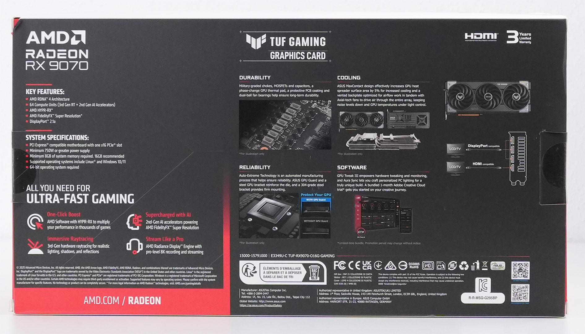
ASUS TUF Gaming Radeon RX 9070 OC is the company's premium custom-design rendition of the new performance segment graphics card from AMD. The new RX 9070 launches today at a starting price of $550, positioned as a value alternative to the top RX 9070 XT part, although for the price at which the ASUS TUF Gaming card is going to market, you should be able to find an RX 9070 XT. This is thanks to the wafer thin $50 gap between the two SKUs, leaving ASUS with no room to squeeze in a premium custom design. The RX 9070 is designed for maxed out gaming at 1440p, including with ray tracing. Not only does it share its $550 MSRP, but also launch date, with the NVIDIA GeForce RTX 5070.

Let's address the elephant in the room, and that is product naming. AMD has made a tactical retreat from the enthusiast segment, wanting to focus instead on the sub-$1,000 performance and mainstream segments. In fact, its top SKU in this generation, the RX 9070 XT, starts only at $600. Both the RX 9070 XT and the RX 9070 we're reviewing here, are named such that consumers compare them to the RTX 5070 Ti and RTX 5070, respectively.
Both cards are based on a common silicon, the Navi 48, which is built on the 4 nm TSMC N4P foundry node. Unlike NVIDIA, made a minor upgrade from the 5 nm TSMC N5. Unlike the 5 nm + 6 nm chiplet-based design of the Navi 32, the Navi 48 is a monolithic 4 nm silicon. The N4P node brings frequency and power advantages over the N5. All generational performance-per-watt uplifts will be attributable not just to the new graphics architecture, but also the fact that the entire silicon—including memory controllers and Infinity Cache—are built on the 4 nm node.
The new RDNA 4 graphics architecture is purpose built for the performance segment, so AMD could pack the most performance at its target price points. The company claims to have achieved significant gains in performance over RDNA 3 in performance per compute unit. The company also posted its biggest generational gains in ray tracing performance, thanks to updated to the RT accelerator; as well as gains in performance of its AI accelerators. In fact, the AI acceleration performance enabled AMD to innovate FSR 4, the biggest upgrade to the company's gaming performance enhancement suite, giving it AI ML-based upscalers and frame generation that offers significant improvements in image quality at every performance preset.
The Radeon RX 9070 is carved out of the Navi 48 silicon by enabling 56 out of 64 compute units present on the silicon, which works out to 3,584 stream processors, 112 AI accelerators, and 56 RT accelerators. The chip also gets 224 TMUs, and the chip's full complement of 128 ROPs, as well as, all 64 MB of Infinity Cache. Perhaps the most striking design choice by AMD is not doing what it did to the RX 7700 XT, and instead giving the RX 9070 the exact same memory configuration as the RX 9070 XT. That's right, you get 16 GB of memory across a 256-bit wide memory interface. What is disappointing, though, is that this is still older generation 20 Gbps GDDR6, which yields 640 GB/s of memory bandwidth. Our recent RTX 5070 testing has shown that memory size trumps bandwidth in ray tracing workloads, and AMD has given the RX 9070 a larger on-die cache than the 48 MB NVIDIA gave the RTX 5070, so things could get interesting.
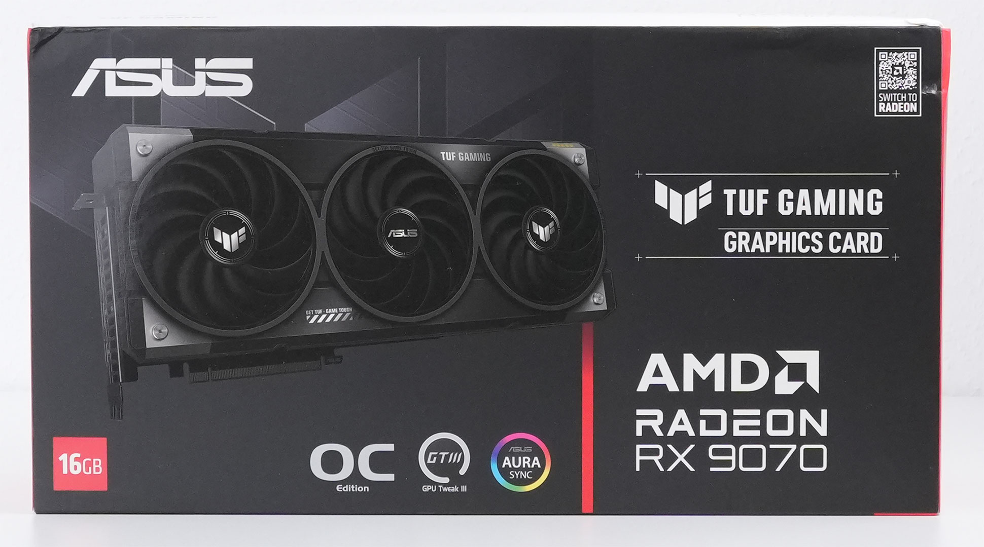
The ASUS TUF Gaming Radeon RX 9070 OC comes with the latest generation TUF Gaming board design that the company introduced with the GeForce RTX 50-series. Given that there is no ROG Strix branded RX 9000 series product, this would be the company's top custom design SKU. Besides a heavy triple-slot cooling solution, the TUF Gaming comes with a generous factory OC of 2170 MHz, up from the 2050 MHz reference. The memory ticks at 20 Gbps (GDDR6 effective). The Vented Exoskeleton cooling solution by ASUS is designed to maximize exposure of the heatsink to the outside, for the best possible ventilation. It also packs three of the latest Axial-Tech fans by the company. ASUS has been unable to provide any pricing for the RX 9070 TUF OC, we estimate it at around $650, and will update this review accordingly, once it's revealed.
| Price | Cores | ROPs | Core Clock | Boost Clock | Memory Clock | GPU | Transistors | Memory | |
|---|---|---|---|---|---|---|---|---|---|
| RTX 3080 | $420 | 8704 | 96 | 1440 MHz | 1710 MHz | 1188 MHz | GA102 | 28000M | 10 GB, GDDR6X, 320-bit |
| RTX 4070 | $490 | 5888 | 64 | 1920 MHz | 2475 MHz | 1313 MHz | AD104 | 35800M | 12 GB, GDDR6X, 192-bit |
| RX 7800 XT | $440 | 3840 | 96 | 2124 MHz | 2430 MHz | 2425 MHz | Navi 32 | 28100M | 16 GB, GDDR6, 256-bit |
| RX 6900 XT | $450 | 5120 | 128 | 2015 MHz | 2250 MHz | 2000 MHz | Navi 21 | 26800M | 16 GB, GDDR6, 256-bit |
| RX 6950 XT | $630 | 5120 | 128 | 2100 MHz | 2310 MHz | 2250 MHz | Navi 21 | 26800M | 16 GB, GDDR6, 256-bit |
| RTX 3090 | $900 | 10496 | 112 | 1395 MHz | 1695 MHz | 1219 MHz | GA102 | 28000M | 24 GB, GDDR6X, 384-bit |
| RTX 4070 Super | $590 | 7168 | 80 | 1980 MHz | 2475 MHz | 1313 MHz | AD104 | 35800M | 12 GB, GDDR6X, 192-bit |
| RX 7900 GRE | $530 | 5120 | 160 | 1880 MHz | 2245 MHz | 2250 MHz | Navi 31 | 57700M | 16 GB, GDDR6, 256-bit |
| RTX 4070 Ti | $700 | 7680 | 80 | 2310 MHz | 2610 MHz | 1313 MHz | AD104 | 35800M | 12 GB, GDDR6X, 192-bit |
| RTX 5070 | $550 | 6144 | 80 | 2325 MHz | 2512 MHz | 1750 MHz | GB205 | 31100M | 12 GB, GDDR7, 192-bit |
| RTX 4070 Ti Super | $750 | 8448 | 112 | 2340 MHz | 2610 MHz | 1313 MHz | AD103 | 45900M | 16 GB, GDDR6X, 256-bit |
| RX 7900 XT | $620 | 5376 | 192 | 2000 MHz | 2400 MHz | 2500 MHz | Navi 31 | 57700M | 20 GB, GDDR6, 320-bit |
| RX 9070 | $550 | 3584 | 128 | 2070 MHz | 2520 MHz | 2518 MHz | Navi 48 | 53900M | 16 GB, GDDR6, 256-bit |
| ASUS RX 9070 TUF OC | $650 (estimated) | 3584 | 128 | 2170 MHz | 2650 MHz | 2518 MHz | Navi 48 | 53900M | 16 GB, GDDR6, 256-bit |
| RX 9070 XT | $600 | 4096 | 128 | 2400 MHz | 2970 MHz | 2518 MHz | Navi 48 | 53900M | 16 GB, GDDR6, 256-bit |
| RTX 3090 Ti | $1000 | 10752 | 112 | 1560 MHz | 1950 MHz | 1313 MHz | GA102 | 28000M | 24 GB, GDDR6X, 384-bit |
| RTX 5070 Ti | $750 | 8960 | 96 | 2295 MHz | 2452 MHz | 1750 MHz | GB203 | 45600M | 16 GB, GDDR7, 256-bit |
| RX 7900 XTX | $820 | 6144 | 192 | 2300 MHz | 2500 MHz | 2500 MHz | Navi 31 | 57700M | 24 GB, GDDR6, 384-bit |
| RTX 4080 | $940 | 9728 | 112 | 2205 MHz | 2505 MHz | 1400 MHz | AD103 | 45900M | 16 GB, GDDR6X, 256-bit |
| RTX 4080 Super | $990 | 10240 | 112 | 2295 MHz | 2550 MHz | 1438 MHz | AD103 | 45900M | 16 GB, GDDR6X, 256-bit |
| RTX 5080 | $1000 | 10752 | 112 | 2295 MHz | 2617 MHz | 1875 MHz | GB203 | 45600M | 16 GB, GDDR7, 256-bit |
| RTX 4090 | $2400 | 16384 | 176 | 2235 MHz | 2520 MHz | 1313 MHz | AD102 | 76300M | 24 GB, GDDR6X, 384-bit |
| RTX 5090 | $2000 | 21760 | 176 | 2017 MHz | 2407 MHz | 1750 MHz | GB202 | 92200M | 32 GB, GDDR7, 512-bit |
AMD RDNA 4 Architecture


The new Radeon RX 9070 XT and RX 9070 are powered by the 4 nm Navi 48 silicon. Unlike Navi 31 and Navi 32 before it, this is a traditional monolithic die built entirely on the TSMC N4P (4 nm EUV) process node. It has an area of 356.5 mm², but with an impressive transistor count of 53.9 billion. To put this number into context, the previous "big Navi" GPU, Navi 31 powering the RX 7900 XTX, has 57.8 billion transistors (just 8% more), despite having 96 CU, a larger Infinity Cache, and a wider 384-bit memory bus. The Navi 31 has a die area of 529 mm² (304 mm² for the 5 nm GCD, with the rest being 6 nm MCDs), so you can see the kind of strides AMD made with die-area. At the top-level, the Navi 48 features a PCI-Express 5.0 x16 host interface, and a 256-bit wide GDDR6 memory bus. With 20 Gbps GDDR6 memory chips, the RX 9070 XT gets 640 GB/s of memory bandwidth. This is made up for with a faster 64 MB Infinity Cache, and a critical improvement AMD made to its memory management system, called Out-of-Order Memory Queuing.
The Navi 48 silicon physically has 64 CU spread across 4 shader engines. With each CU containing 64 stream processors, the chip has a total of 4,096 stream processors. All 64 CU are enabled on the RX 9070 XT, while the RX 9070 has 56 out of 64 of them enabled. The maxed-out Navi 48 contains 4,096 stream processors, 128 AI accelerators, 64 RT accelerators, 256 TMUs, and 128 ROPs. The chip also features 64 MB of 3rd Gen Infinity Cache, and a 256-bit wide GDDR6 memory interface, driving 16 GB of 20 Gbps memory on both the RX 9070 XT and RX 9070. With 56 CU enabled on the RX 9070, it has 3,584 stream processors, 112 AI accelerators, 56 RT accelerators, 224 TMUs, and an untouched ROP count of 128, besides the exact same memory configuration as the RX 9070 XT.

At the heart of the RDNA 4 graphics architecture is the new dual compute unit, with a vastly improved memory sub-system, improvements made to the scalar units, a new technology called dynamic register allocation, and improvements to CU efficiency and engine clocks. Each CU has two scheduler blocks, driving a 192 KB general purpose register (GPR), an 8 KB scalar GPR, 32 FMA ALUs, and 32 FMA+INT ALUs. There are also 8 transcendental logic units. RDNA 4 introduces the concept of dual SIMD32 vector units, for even more parallelism. The Scalar Unit comes with support for newer Float32 ops. Schedulers are updated with accelerated spill/fill operations. Instruction prefetching is improved. The new generation AI Accelerator comes with two 16-bit and four 8-bit/4-bit dense matrix compute rates, support for 4:2 structured sparsity for doubling throughput, and matrix loads with transpose. AMD has incorporated many technologies from its CDNA 3 Instinct AI ML accelerators on the AI Accelerators of RDNA 4, including enhanced and power-optimized WMMA, improvements to the ops per CU, support for FP8, E4M3 and E5M2 formats, and 4:2 structured sparsity.

The new generation AI Accelerator comes with two 16-bit and four 8-bit/4-bit dense matrix compute rates, support for 4:2 structured sparsity for doubling throughput, and matrix loads with transpose. AMD has incorporated many technologies from its CDNA 3 Radeon Instinct AI ML accelerators on the AI Accelerators of RDNA 4, including enhanced and power-optimized WMMA, improvements to the ops per CU, support for FP8, E4M3 and E5M2 formats, and 4:2 structured sparsity.


The new generation Ray Accelerator comes with double the box and triangle intersection resources as RDNA 3 RT accelerator, support for hardware instance transforms, improvements to the RT stack management, BVH8 node compression, and a revolutionary feature called oriented bounding boxes. To contain the number of rays really needed to be tested against an object, modern ray tracing technologies use something called a bounding box, which defines a region in which a geometry has to be tested against rays. Most of the time, the geometry is of a vastly different shape and smaller than the shape of a bounding box, which introduces false intersections, and wastes ray testing resources. AMD innovated a way to turn this bounding box into a 3D shape by giving it a Z-axis component, so the bounding box is oriented closer to the shape of the object to be tested, reducing the number of rays needed to be tested against it.

This graph highlights the contribution of various components toward the 100% generational ray traversal performance gain, allowing AMD to make do with a CU count of 64, with RDNA 3 being the baseline.

Both ray tracing and ML acceleration are memory sensitive applications, and so AMD innovated a revolutionary change to its memory management system, with the introduction of new out-of-order memory. All math is executed in waves on an RDNA GPU, and mutual dependencies between waves can cause memory request stream misses, as one wave's memory request queue waits for the other wave to complete its task. This is solved with a new out-of-order (relaxed ordering) memory management. This graph highlights the contribution of various components toward the 100% generational ray traversal performance gain, allowing AMD to make do with a CU count of 64, with RDNA 3 being the baseline.

On AMD, a fairly big chunk of the ray tracing stack continues to be executed on shaders, but the company has made advances to ensure the cost of ray tracing on the shader resources of the GPU, with the introduction of Dynamic Registers, to improve parallelism.

The new Radiance 2 Display Engine comes with major hardware updates that reduce GPU idle power draw in multi-monitor setups. The engine also comes with hardware flip-metering support (something NVIDIA also introduced with Blackwell, and which enables Multi-Frame Gen on the RTX 50-series). Flip-metering improves video frame pacing to the GPU and reduces CPU overhead for video playback. There is also a display engine level hardware image sharpening component that drives Radeon Image Sharpening. As for I/O, you get contemporary DisplayPort 2.1a and HDMI 2.1b, the maximum bitrate is UHBR 13.5.

Navi 48 comes with a dual media engine, each of the two can perform concurrent encoding and decoding, and so the implementation resembles an NVIDIA GPU having two each of NVENC and NVDEC units. The new generation media engine offers a 25% increase in H.264 low-latency encode quality, and an 11% improvement in HEVC encode quality. AV1 encode and decode get B-frames support, vastly improving bitrates. The media engine posts a 50% generational performance uplift (measured in encoder/decoder frame rates), with reductions in memory overhead.
AMD FSR 4 and New AMD Software Features
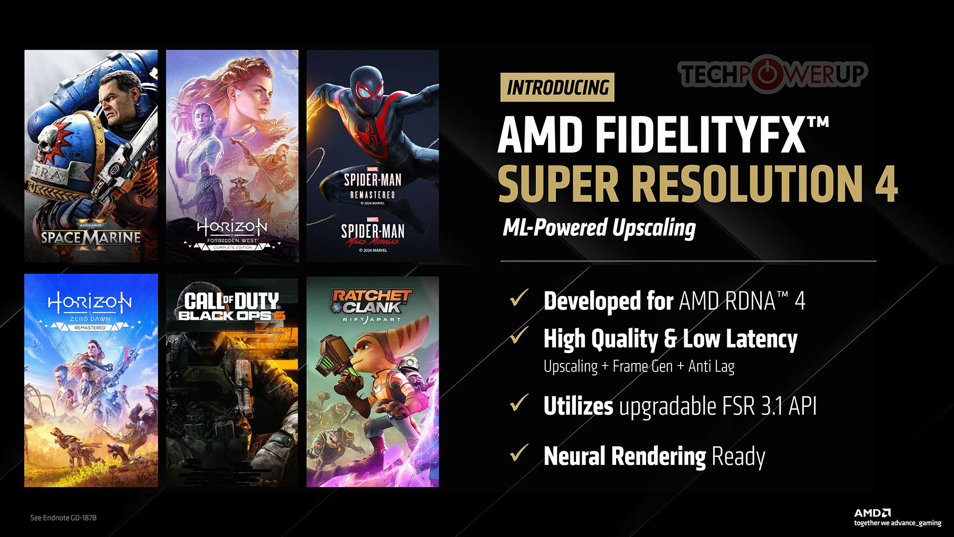

With the Radeon RX 9000 series, AMD is debuting FSR 4, the latest version of its performance enhancement suite. FSR 4 introduces the biggest tech update since FSR 2, which also makes it exclusive to the RX 9000 series. With the RDNA 4 generation of GPUs offering significantly higher ML compute throughput, AMD designed a new ML-based upscaler to reconstruct details of the upscaled frame. In that sense, FSR 4 is technologically close to DLSS. RDNA 4 GPUs also leverage AI DNNs to de-noise ray tracing and path tracing, unburdening the shaders.
An AI ML based upscaler requires ground truth data, and just as NVIDIA goes through the painstaking task of training game-specific ML models that can later be shipped to end-users through game developers and as driver updates; AMD has set up a large FSR 4 data-center of its own, powered by Radeon Instinct MI300-series AI GPUs for the task. On the client side, the ML-based upscaler needs the dedicated AI acceleration hardware from the RDNA 4 family. The frame generation technology appears to be carried over from FSR 3 Frame Generation, and is essentially a smart frame interpolation technology.

AMD in its presentation provided examples of image quality for FSR 4, claiming that in some cases, FSR 4 presents geometry more accurately than even native resolution. While AMD didn't detail it, FSR 4 comes with preparation for neural rendering. Given that Microsoft has now standardized neural shaders, and the ability for applications to directly address AI acceleration hardware on the GPU via the DirectX API, AMD could in the near future implement neural rendering, however, the company hasn't detailed a timeline. FSR 4 is ready for neural rendered objects.
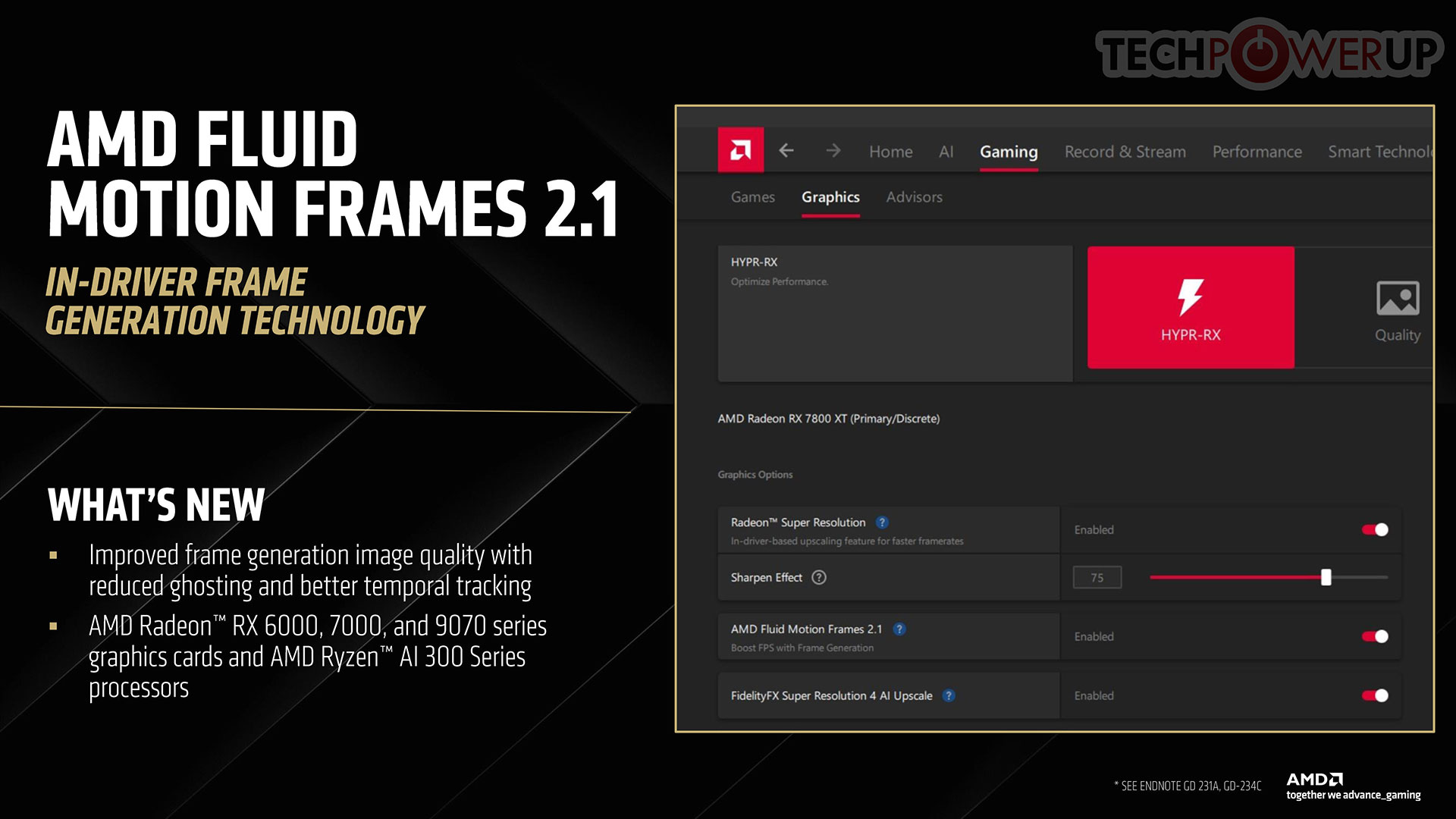
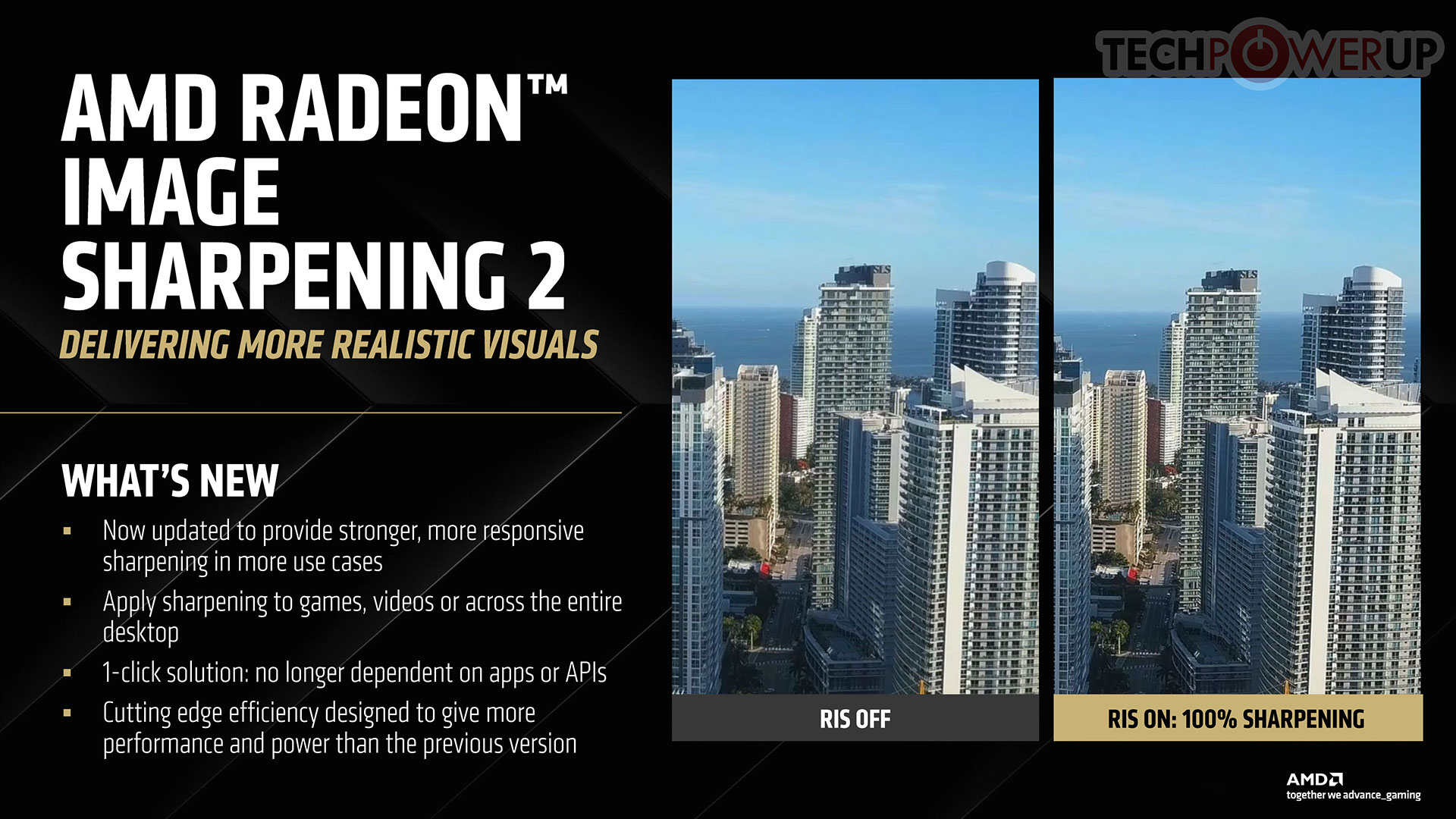
Fluid Motion Frames gets an update with FMF 2.1, with improved image quality, reduced ghosting, and improved temporal tracking. The company also updated its API-agnostic image sharpening tool, with the introduction of Radeon Image Sharpening 2 (RIS 2).

AMD provides a slick driver frontend application called simply "AMD Software." AMD improved the way in which users can report bugs, artifacts, or corruption in games, through a voluntary (opt-in) feature called AMD Image Inspector.


As you submit a screenshot or video sequence to AMD, the company uses an AI model to identify rendering bugs, or corruption in the display. The entire driver-level game optimization, testing, and bug fixing process has been revamped with AI doing the heavy lifting.
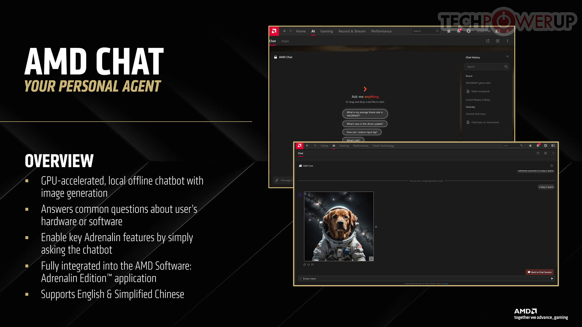
The company also introduced AMD Chat, which is an AI chatbot that runs locally, and is accelerated by the GPU. You can make plain language queries on configuring AMD Software features and settings; and also chat with it on AMD technologies. This is essentially AMD's answer to NVIDIA's ChatRTX, but we don't know if the utility can be trained with custom datasets.
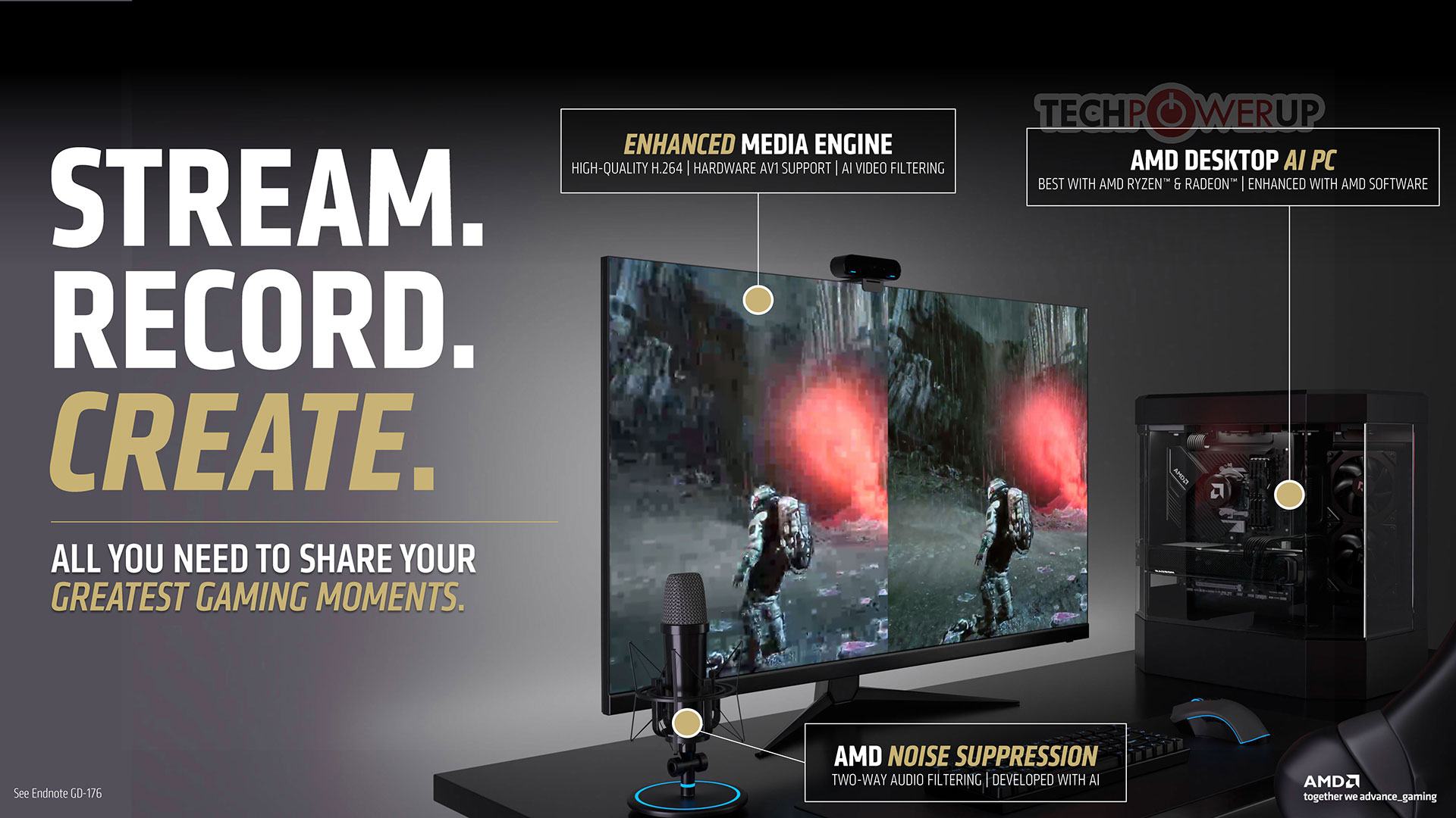
For streamers, AMD Software simplifies connecting their gameplay with their social media and streaming accounts. You can then take advantage of the new dual media engine of RDNA 4 that improves H.264 and HEVC image quality, and use other utilities such as AMD Noise Suppression, which is a 2-way AI-based audio filter.
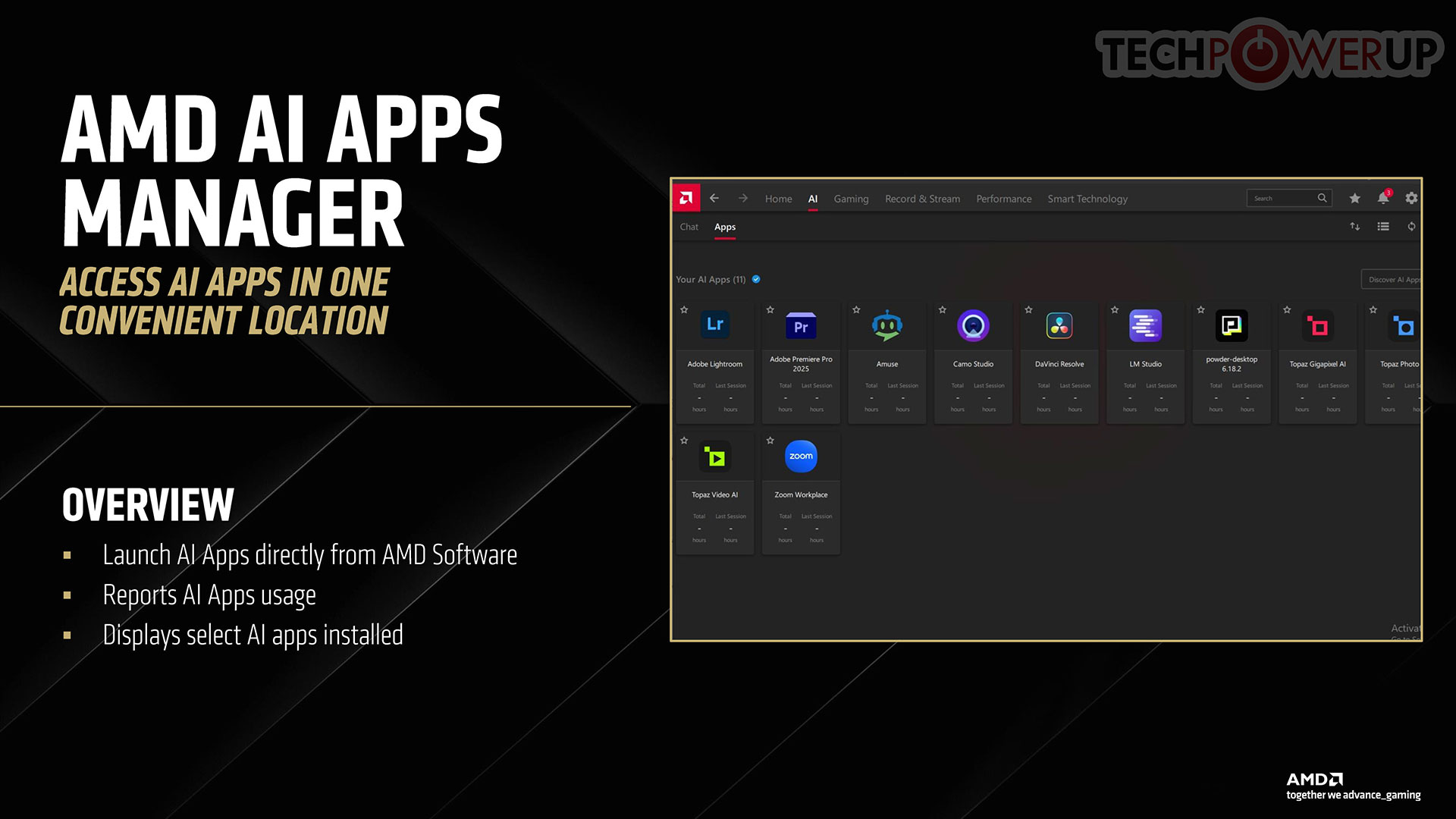
AMD AI Apps Manager consolidates all your AI applications into a simple launcher-like interface resembling a game launcher.
Packaging
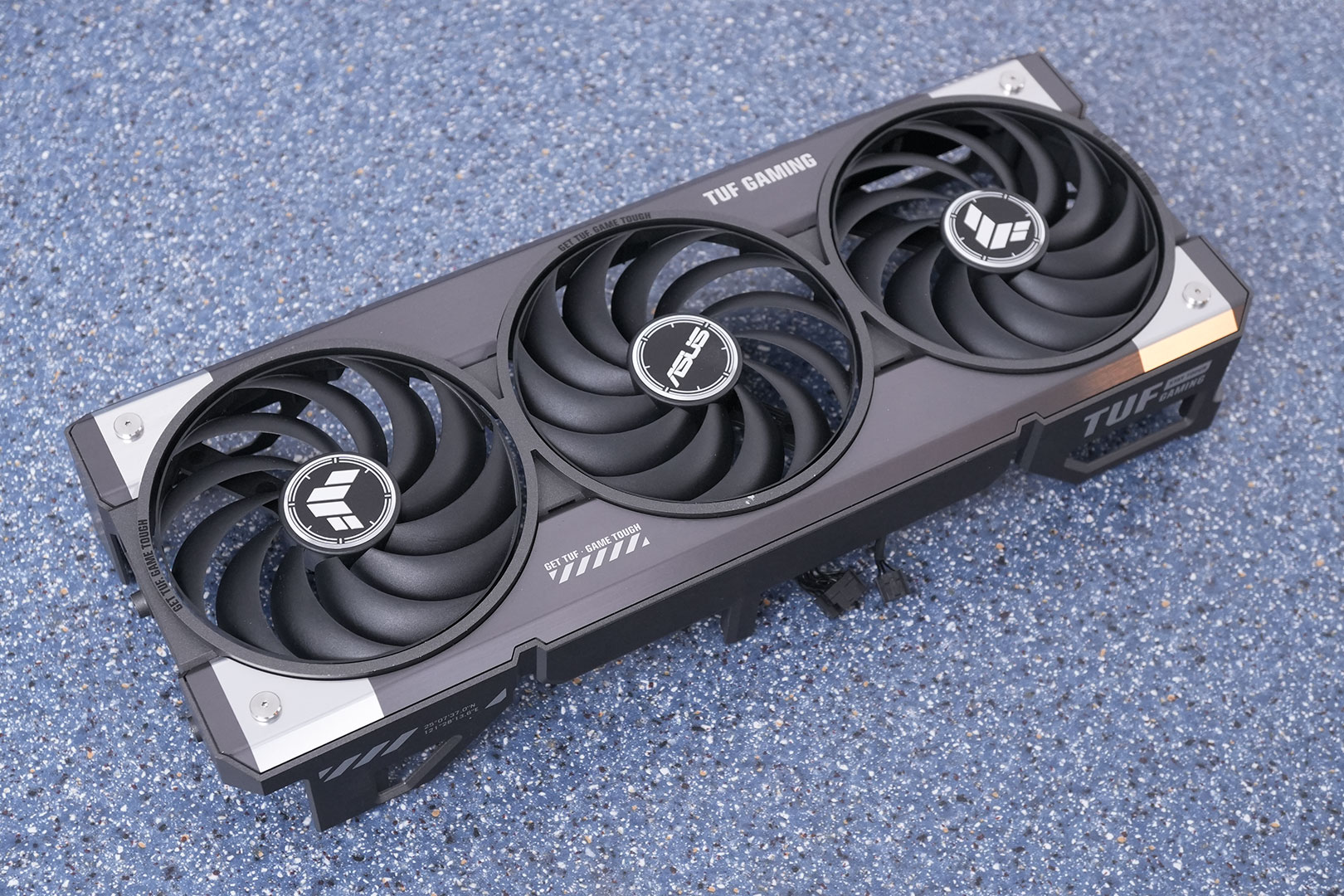
The Card
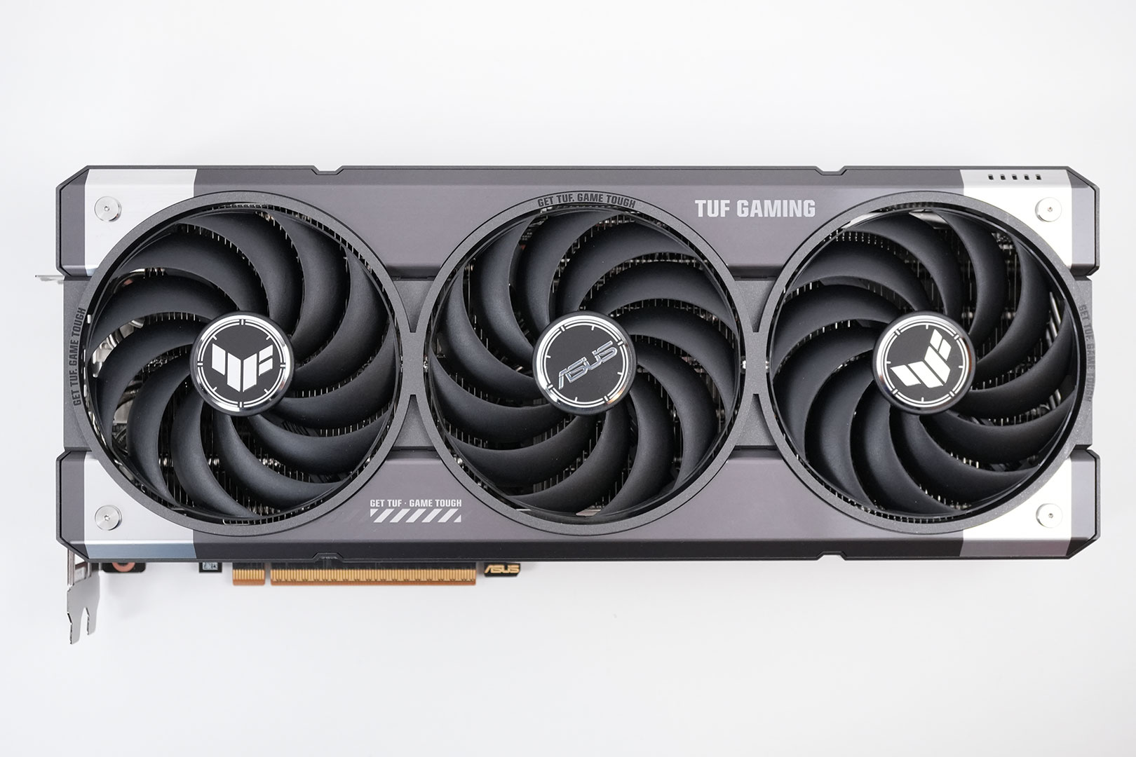
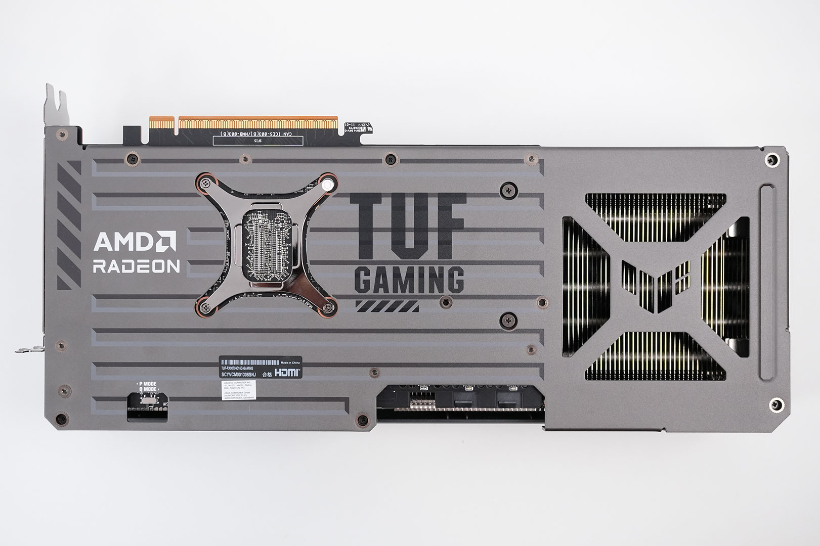
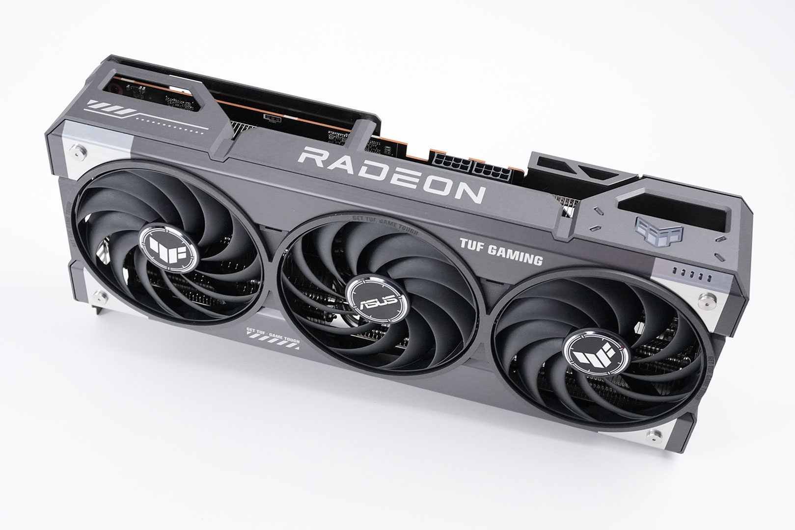
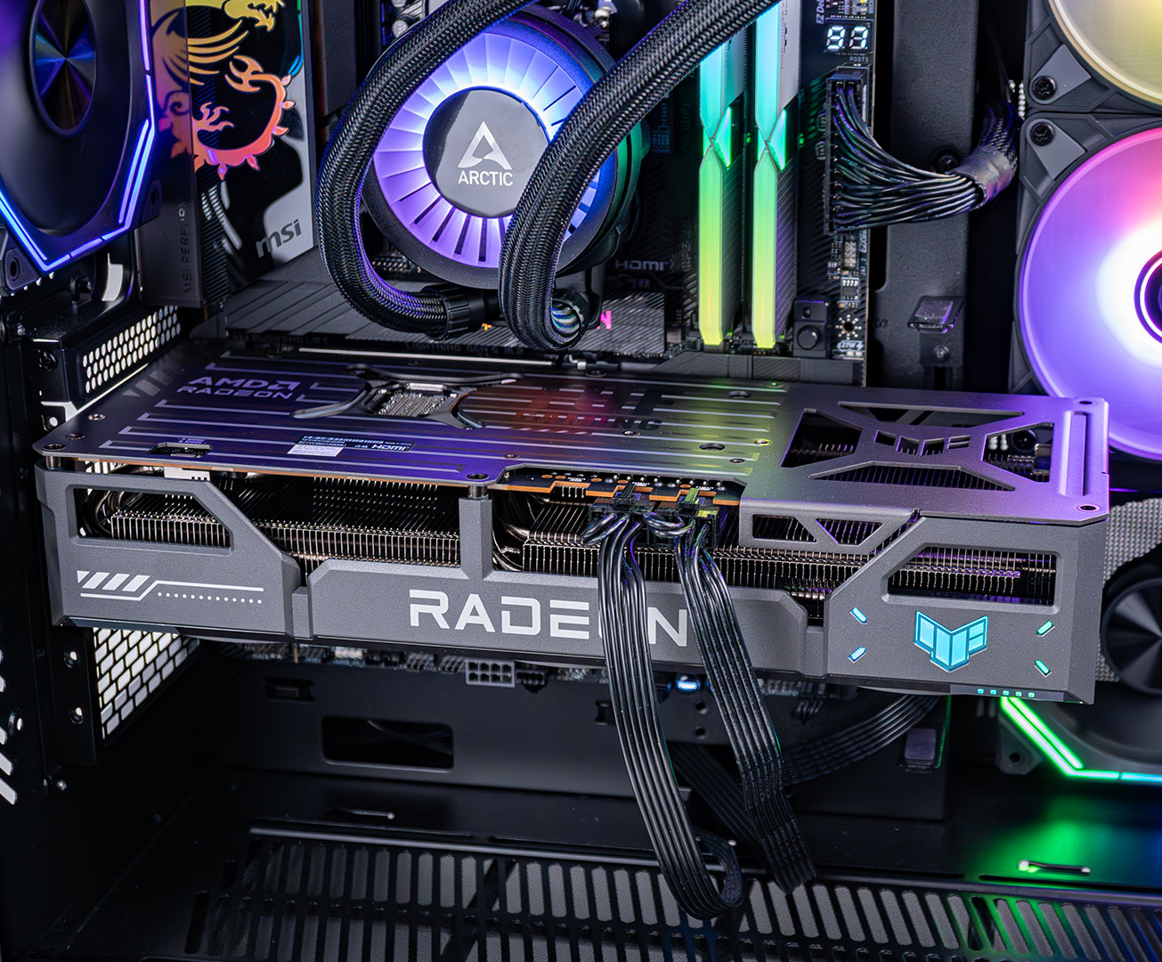
Visually, the ASUS RTX 9070 TUF OC follows the design theme of the company's previous TUF cards, and it also matches the GeForce 50 TUF visuals exactly. On the back you get a high quality metal backplate with a cutout for air to flow through.
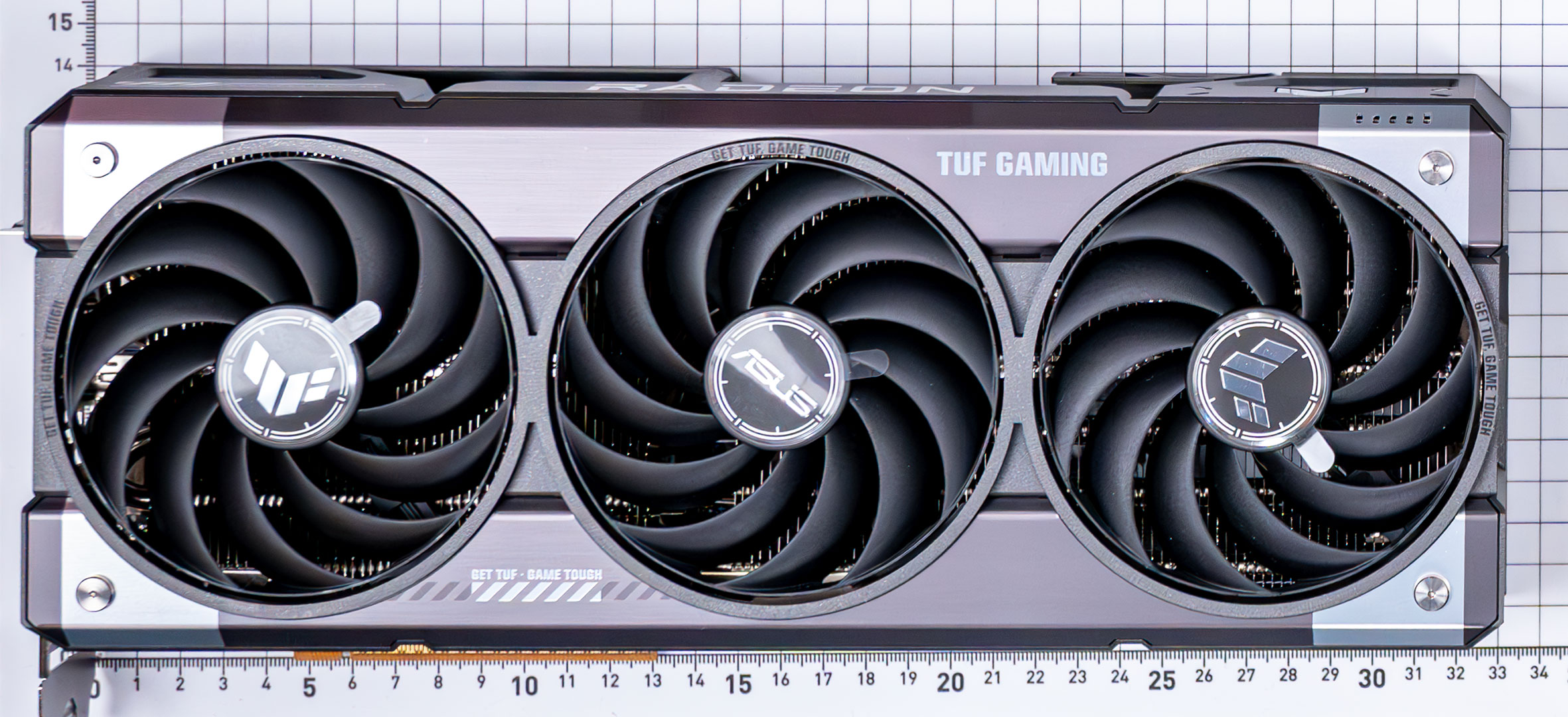
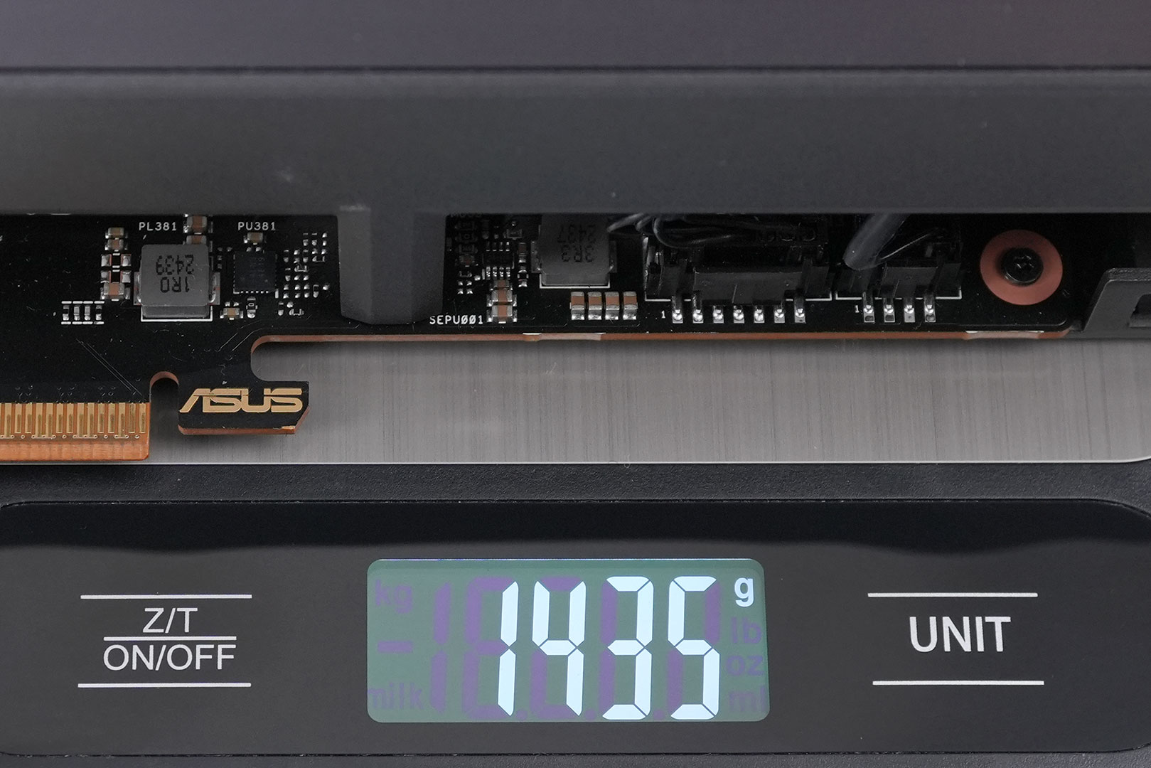
Dimensions of the card are 33.0 x 14.0 cm, and it weighs 1435 g.
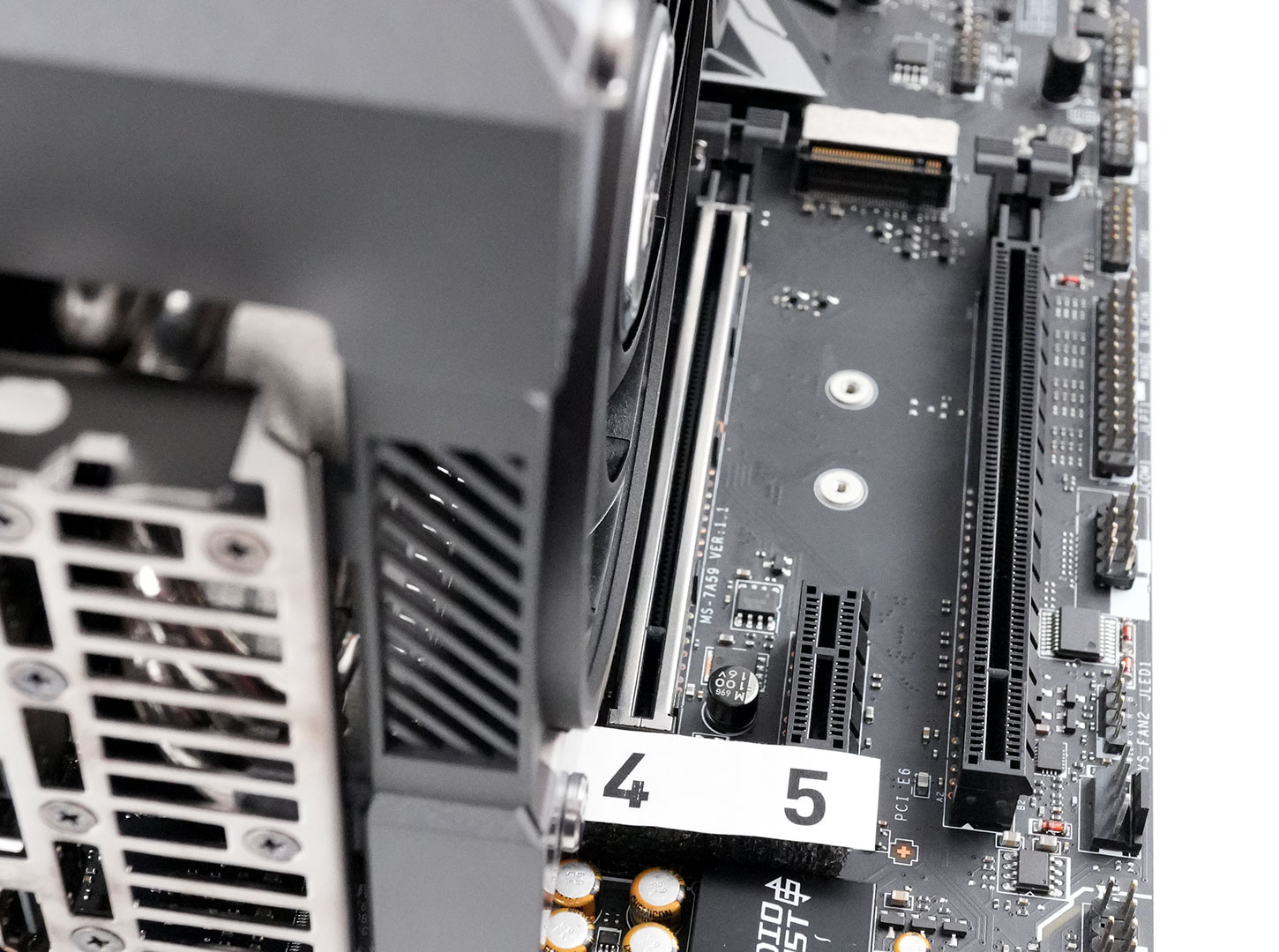
Installation requires three slots in your system. We measured the card's width to be 60 mm.
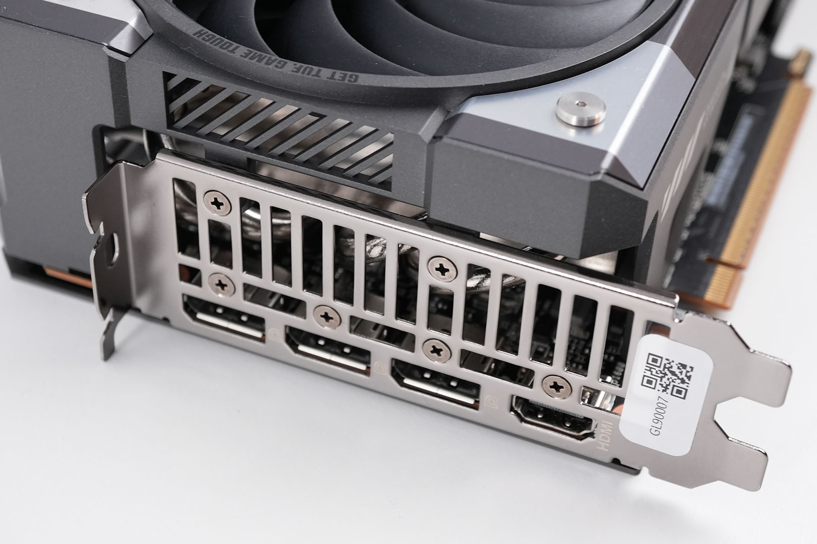
Display connectivity includes three standard DisplayPort 2.1a and a HDMI 2.1b.
With RDNA 4, AMD put effort to improve its standing with game streamers and creative professionals. It's done this by giving Navi 48 a dual VCN solution, so the GPU has two concurrent hardware accelerators for encoding and decoding. Perhaps the biggest changes at the silicon level is that AMD improved the encoding quality of its hardware H.264 and HEVC codecs. This was a niche complaint streamers had with AMD GPUs, and would avoid the brand altogether. The company also updated its AV1 hardware acceleration with support for B-frames, which are frames that lack image information, but math data that let the decoder reconstruct image data by comparing with the image data from adjacent I-frames containing it. This technique vastly improves streaming bitrates since half the frames lack image data.
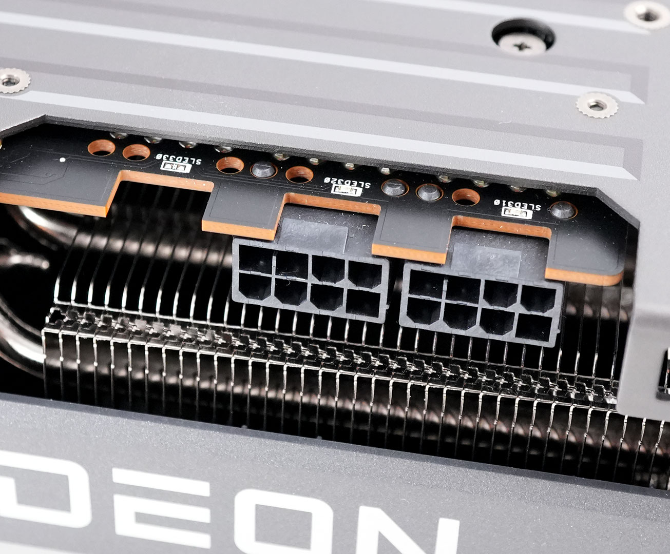
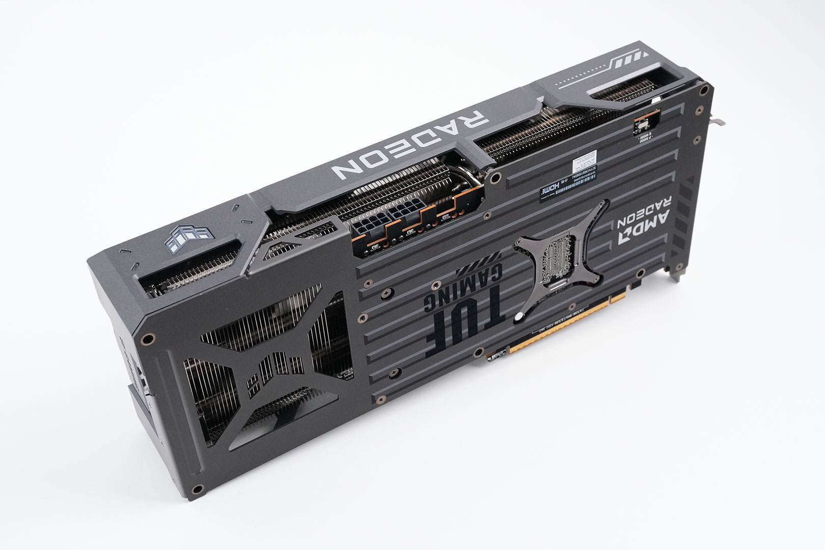
The card uses two 8-pin power connectors, which allow a total power consumption of 300 W, plus 75 W from the PCIe slot.
ASUS has installed an RGB lighting zone near the corner of the card.
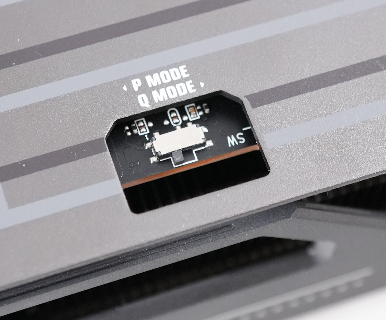
This BIOS switch lets you toggle between the default performance BIOS and an optional "quiet" BIOS.
Teardown
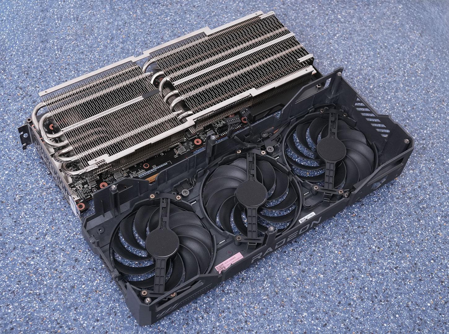
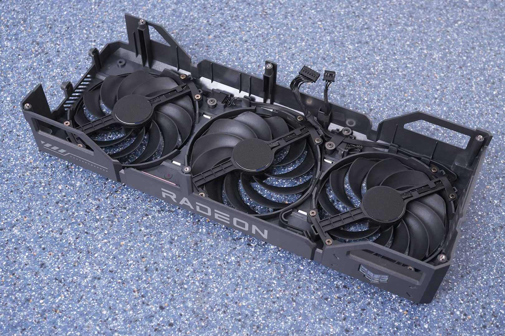
ASUS made the fan assembly removable, so it's easy to replace a fan if one breaks in a few years.
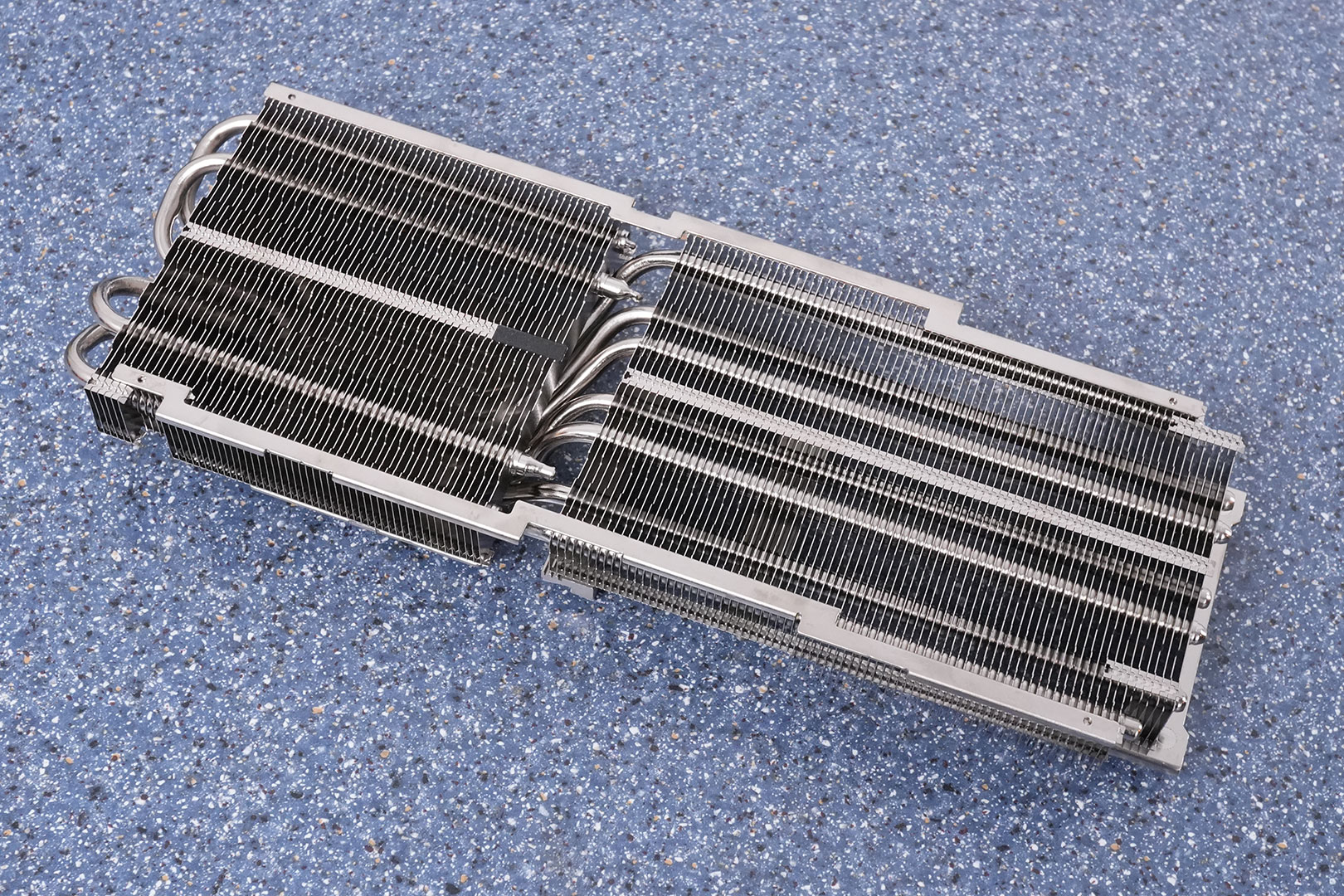
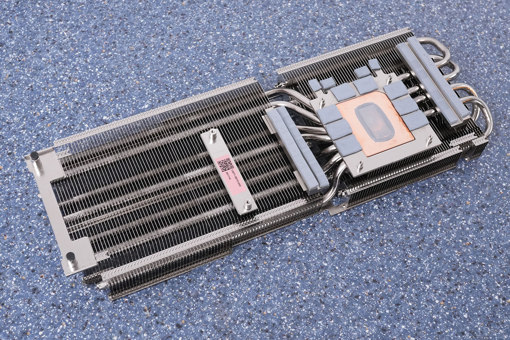
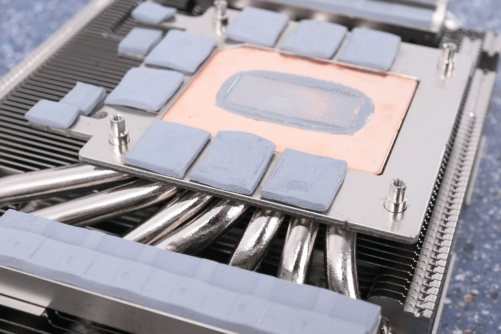
The heatsink uses seven heatpipes and provides cooling not only for the GPU, but also for the memory chips and VRM circuitry.
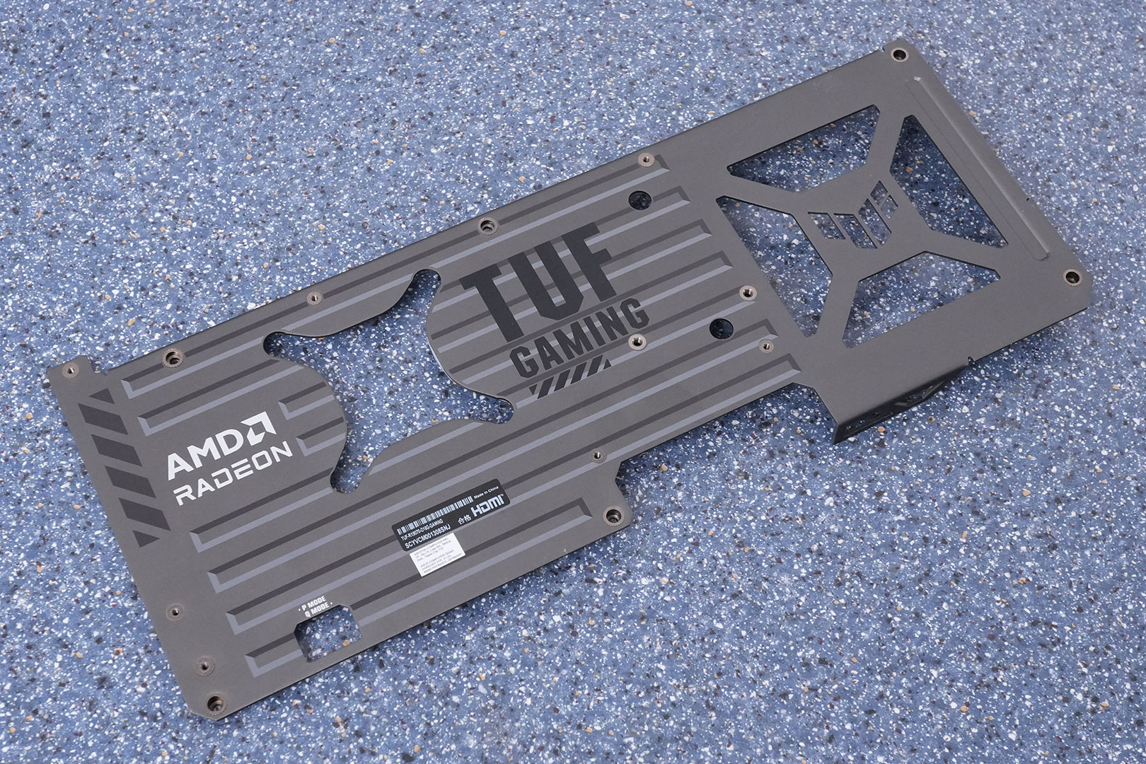

The backplate protects against damage during installation and handling.
Our Patreon Silver Supporters can read articles in single-page format.
Apr 12th, 2025 20:56 EDT
change timezone
Latest GPU Drivers
New Forum Posts
- Bought a Sapphire RX 7900 XT and..... (4)
- What is going to be your next tech upgrade? just curious :) (21)
- X79 and/or rampage IV OC'ing thread for those of us still left.... (2395)
- Is RX 9070 VRAM temperature regular value or hotspot? (346)
- Cache Ratio stuck at 600hz lower than Turbo Cores with Ring Down Bin on (4)
- best ram to buy for my usage and system specs? (14)
- Lossless scaling (18)
- works and stops, random colored screens, Biostar RX560 896SPs (2)
- Steam Deck Owners Clubhouse (509)
- AMD Radeon Pro v540 Research Thread (295)
Popular Reviews
- Thermaltake TR100 Review
- The Last Of Us Part 2 Performance Benchmark Review - 30 GPUs Compared
- TerraMaster F8 SSD Plus Review - Compact and quiet
- Zotac GeForce RTX 5070 Ti Amp Extreme Review
- ASUS GeForce RTX 5080 TUF OC Review
- ASRock Z890 Taichi OCF Review
- Sapphire Radeon RX 9070 XT Pulse Review
- Sapphire Radeon RX 9070 XT Nitro+ Review - Beating NVIDIA
- Upcoming Hardware Launches 2025 (Updated Apr 2025)
- MSI MAG CORELIQUID A15 360 Review
Controversial News Posts
- NVIDIA GeForce RTX 5060 Ti 16 GB SKU Likely Launching at $499, According to Supply Chain Leak (181)
- MSI Doesn't Plan Radeon RX 9000 Series GPUs, Skips AMD RDNA 4 Generation Entirely (146)
- Microsoft Introduces Copilot for Gaming (124)
- NVIDIA Sends MSRP Numbers to Partners: GeForce RTX 5060 Ti 8 GB at $379, RTX 5060 Ti 16 GB at $429 (121)
- Nintendo Confirms That Switch 2 Joy-Cons Will Not Utilize Hall Effect Stick Technology (105)
- Over 200,000 Sold Radeon RX 9070 and RX 9070 XT GPUs? AMD Says No Number was Given (100)
- Nintendo Switch 2 Launches June 5 at $449.99 with New Hardware and Games (99)
- NVIDIA PhysX and Flow Made Fully Open-Source (77)