 4
4
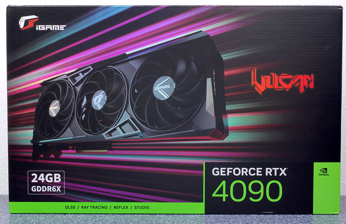
Colorful GeForce RTX 4090 Vulcan OC-V Review
(4 Comments) »Introduction
Colorful GeForce RTX 4090 Vulcan OC-V represents the company's top air-cooled custom-design RTX 4090 "Ada" graphics card, which we're thrilled to review for you today, besides more than half a dozen other custom-design cards. It isn't a Colorful product without having over-the-top styling, some of the heaviest cooling solutions with the most elaborate designs; and a loaded accessories package; and the same holds true for the RTX 4090 Vulcan OC-V. Colorful has looked after everything a gamer and PC enthusiast could possibly want, and turned it into a checklist when designing this card.

The GeForce RTX 4090 "Ada" represents this generation's flagship graphics card from NVIDIA, and is the company's latest attempt at creating a GPU that's as generationally fast and capable as if Moore's Law were supporting its development (it isn't). You are promised nearly 50% performance gains over the previous-gen RTX 3090, and nearly 100% if you consider the RTX 3080 as last-generation's flagship, which NVIDIA did.
The "Ada Lovelace" architecture heralds the third generation NVIDIA RTX, the company's path-breaking real time ray tracing technology that combines conventional raster 3D graphics with real time ray traced elements such as lighting, shadows, reflections, illumination, and motion-blur. Over the generations, NVIDIA has innovated fixed-function ray tracing hardware for pretty much each kind of RT workload, and the same holds true for "Ada." In addition to these, NVIDIA innovated the Optical Flow Accelerator, a hardware component that enables the GPU to create unique frames out of thin air, using AI, without involving the bulk of the raster graphics machinery.
NVIDIA carved the RTX 4090 out of the 5 nm AD102 silicon by enabling 16,384 out of 18.432 CUDA cores physically present, besides 128 3rd generation RT cores, 512 4th generation Tensor cores, 512 TMUs, and 192 ROPs. The memory subystem looks identical to the RTX 3090 Ti, with 24 GB of 21 Gbps GDDR6X memory across a 384-bit memory bus; but NVIDIA has significantly enlarged the on-die cache memory with "Ada."
The Colorful RTX 4090 Vulcan OC-V comes with not just the company's most premium VRM design and level of PCB engineering, but also some really cool features, including a color LCD screen that puts out real-time graphics card monitoring (or anything you want it to); dual-BIOS, RGB headers, besides some goodies in the box. The card comes with factory-overclocked speeds of 2.62 GHz, compared to 2.52 GHz reference. Colorful is pricing the card at $1,770, a $170 (+10%) premium over the NVIDIA baseline price.
| Price | Cores | ROPs | Core Clock | Boost Clock | Memory Clock | GPU | Transistors | Memory | |
|---|---|---|---|---|---|---|---|---|---|
| RTX 2080 | $400 | 2944 | 64 | 1515 MHz | 1710 MHz | 1750 MHz | TU104 | 13600M | 8 GB, GDDR6, 256-bit |
| RTX 3060 Ti | $450 | 4864 | 80 | 1410 MHz | 1665 MHz | 1750 MHz | GA104 | 17400M | 8 GB, GDDR6, 256-bit |
| RX 6700 XT | $410 | 2560 | 64 | 2424 MHz | 2581 MHz | 2000 MHz | Navi 22 | 17200M | 12 GB, GDDR6, 192-bit |
| RX 6750 XT | $470 | 2560 | 64 | 2495 MHz | 2600 MHz | 2250 MHz | Navi 22 | 17200M | 12 GB, GDDR6, 192-bit |
| RTX 2080 Ti | $550 | 4352 | 88 | 1350 MHz | 1545 MHz | 1750 MHz | TU102 | 18600M | 11 GB, GDDR6, 352-bit |
| RTX 3070 | $530 | 5888 | 96 | 1500 MHz | 1725 MHz | 1750 MHz | GA104 | 17400M | 8 GB, GDDR6, 256-bit |
| RTX 3070 Ti | $600 | 6144 | 96 | 1575 MHz | 1770 MHz | 1188 MHz | GA104 | 17400M | 8 GB, GDDR6X, 256-bit |
| RX 6800 | $580 | 3840 | 96 | 1815 MHz | 2105 MHz | 2000 MHz | Navi 21 | 26800M | 16 GB, GDDR6, 256-bit |
| RX 6800 XT | $600 | 4608 | 128 | 2015 MHz | 2250 MHz | 2000 MHz | Navi 21 | 26800M | 16 GB, GDDR6, 256-bit |
| RTX 3080 | $660 | 8704 | 96 | 1440 MHz | 1710 MHz | 1188 MHz | GA102 | 28000M | 10 GB, GDDR6X, 320-bit |
| RTX 3080 Ti | $850 | 10240 | 112 | 1365 MHz | 1665 MHz | 1188 MHz | GA102 | 28000M | 12 GB, GDDR6X, 384-bit |
| RX 6900 XT | $680 | 5120 | 128 | 2015 MHz | 2250 MHz | 2000 MHz | Navi 21 | 26800M | 16 GB, GDDR6, 256-bit |
| RX 6950 XT | $950 | 5120 | 128 | 2100 MHz | 2310 MHz | 2250 MHz | Navi 21 | 26800M | 16 GB, GDDR6, 256-bit |
| RTX 3090 | $950 | 10496 | 112 | 1395 MHz | 1695 MHz | 1219 MHz | GA102 | 28000M | 24 GB, GDDR6X, 384-bit |
| RTX 3090 Ti | $1200 | 10752 | 112 | 1560 MHz | 1950 MHz | 1313 MHz | GA102 | 28000M | 24 GB, GDDR6X, 384-bit |
| RTX 4090 | $1600 | 16384 | 176 | 2235 MHz | 2520 MHz | 1313 MHz | AD102 | 76300M | 24 GB, GDDR6X, 384-bit |
| Colorful RTX 4090 Vulcan OC-V | $1770 | 16384 | 176 | 2235 MHz | 2520 MHz | 1313 MHz | AD102 | 76300M | 24 GB, GDDR6X, 384-bit |
GeForce Ada Architecture
The Ada graphics architecture heralds the third generation of the NVIDIA RTX technology, an effort toward increasing the realism in game visuals by leveraging real-time ray tracing, without the enormous amount of compute power required to draw purely ray-traced 3D graphics. This is done by blending conventional raster graphics with ray traced elements such as reflections, lighting, and global illumination, to name a few. The 3rd generation of RTX heralds the new higher IPC "Ada" CUDA core, 3rd generation RT core, 4th generation Tensor core, and the new Optical Flow Processor, a component that plays a key role in generating new frames without involving the GPU's main graphics rendering pipeline.


The GeForce Ada graphics architecture driving the RTX 4090 leverages the TSMC 5 nm EUV foundry process to increase transistor counts to a mammoth 76.3 billion transistors, a nearly 3-fold increase over the previous-generation; while the die-size is actually smaller at 608 mm², compared to 628 mm² of the previous-generation GA102. The GPU features a PCI-Express 4.0 x16 host interface, and a 384-bit wide GDDR6X memory bus wired out to 24 GB of GDDR6X memory. The Optical Flow Accelerator (OFA) is an independent top-level component. The chip features two NVENC and one NVDEC units in the GeForce RTX 40-series; while future professional-visualization graphics cards will have all six each of the NVENC and NVDEC components enabled.
The essential component hierarchy is similar to past generations of NVIDIA GPUs. The AD102 silicon features a whopping 12 Graphics Processing Clusters (GPCs), each of these has all the SIMD and graphics rendering machinery, and is a small GPU in its own right. Each GPC shares a raster engine (geometry processing components) and two ROP partitions (each with eight ROP units). The GPC of the AD102 contains six Texture Processing Clusters (TPCs), the main number-crunching machinery. Each of these has two Streaming Multiprocessors (SM), and a Polymorph unit. Each SM contains 128 CUDA cores across four partitions. Half of these CUDA cores are pure-FP32; while the other half is capable of FP32 or INT32. The SM retains concurrent FP32+INT32 math processing capability. The SM also contains a 3rd generation RT core, four 4th generation Tensor cores, some cache memory, and four TMUs. There are 12 SM per GPC, so 1,536 CUDA cores, 48 Tensor cores, and 12 RT cores; per GPC. Twelve GPCs hence add up to 18,432 CUDA cores, 576 Tensor cores, and 144 RT cores. Each GPC contributes 16 ROPs, so there are a mammoth 192 ROPs on the silicon. A 96 MB L2 cache serves as town-square for the various GPCs, memory controllers, and the PCIe host interface, to exchange data. NVIDIA carved the RTX 4090 out of the AD102 by disabling one of the twelve GPCs, and a further two TPCs from two of the other GPCs, as shown in the red-shaded parts of the block diagram above. The RTX 4090 has 72 MB L2 cache enabled (out of 96 MB physically present on the silicon).


The 3rd generation RT core accelerates the most math-intensive aspects of real-time ray tracing, including BVH traversal. Displaced micro-mesh engine is a revolutionary feature introduced with the new 3rd generation RT core, which accelerates the displaced micro-mesh feature. Just as mesh shaders and tessellation have had a profound impact on improving performance with complex raster geometry, allowing game developers to significantly increase geometric complexity; DMMs is a method to reduce the complexity of the bounding-volume hierarchy (BVH) data-structure, which is used to determine where a ray hits geometry. Previously the BVH had to capture even the smallest details to properly determine the intersection point. Ada's ray tracing architecture receives a major performance uplift from Shader Execution Reordering (SER), a software-defined feature that requires awareness from game-engines, to help the GPU reorganize and optimize worker threads associated with ray tracing.


The BVH now needn't have data for every single triangle on an object, but can represent objects with complex geometry as a coarse mesh of base triangles, which greatly simplifies the BVH data structure. A simpler BVH means less memory consumed and helps to greatly reduce ray tracing CPU load, because the CPU only has to generate a smaller structure. With older "Ampere" and "Turing" RT cores, each triangle on an object had to be sampled at high overhead, so the RT core could precisely calculate ray intersection for each triangle. With Ada, the simpler BVH, plus the displacement maps can be sent to the RT core, which is now able to figure out the exact hit point on its own. NVIDIA has seen 11:1 to 28:1 compression in total triangle counts. This reduces BVH compile times by 7.6x to over 15x, in comparison to the older RT core; and reducing its storage footprint by anywhere between 6.5 to 20 times. DMMs could reduce disk- and memory bandwidth utilization, utilization of the PCIe bus, as well as reduce CPU utilization. NVIDIA worked with Simplygon and Adobe to add DMM support for their tool chains.


Opacity Micro Meshes (OMM) is a new feature introduced with Ada to improve rasterization performance, particularly with objects that have alpha (transparency data). Most low-priority objects in a 3D scene, such as leaves on a tree, are essentially rectangles with textures on the leaves where the transparency (alpha) creates the shape of the leaf. RT cores have a hard time intersecting rays with such objects, because they're not really in the shape that they appear (they're really just rectangles with textures that give you the illusion of shape). Previous-generation RT cores had to have multiple interactions with the rendering stage to figure out the shape of a transparent object, because they couldn't test for alpha by themselves.


This has been solved by using OMMs. Just as DMMs simplify geometry by creating meshes of micro-triangles; OMMs create meshes of rectangular textures that align with parts of the texture that aren't alpha, so the RT core has a better understanding of the geometry of the object, and can correctly calculate ray intersections. This has a significant performance impact on shading performance in non-RT applications, too. Practical applications of OMMs aren't just low-priority objects such as vegetation, but also smoke-sprites and localized fog. Traditionally there was a lot of overdraw for such effects, because they layered multiple textures on top of each other, that all had to be fully processed by the shaders. Now only the non-opaque pixels get executed—OMMs provide a 30 percent speedup with graphics buffer fill-rates, and a 10 percent impact on frame-rates.


DLSS 3 introduces a revolutionary new feature that promises a doubling in frame-rate at comparable quality, it's called AI frame-generation. While it has all the features of DLSS 2 and its AI super-resolution (scaling up a lower-resolution frame to native resolution with minimal quality loss); DLSS 3 can generate entire frames simply using AI, without involving the graphics rendering pipeline.


Every alternating frame with DLSS 3 is hence AI-generated, without being a replica of the previous rendered frame. This is possible only on the Ada graphics architecture, because of a hardware component called the optical flow accelerator (OFA), which assists in predicting what the next frame could look like, by creating what NVIDIA calls an optical flow-field. OFA ensures that the DLSS 3 algorithm isn't confused by static objects in a rapidly-changing 3D scene (such as a race sim). The process heavily relies on the performance uplift introduced by the FP8 math format of the 4th generation Tensor core. A third key ingredient of DLSS 3 is Reflex. By reducing the rendering queue to zero, Reflex plays a vital role in ensuring that frame-times with DLSS 3 are at an acceptable level, and a render-queue doesn't confuse the upscaler. A combination of OFA and the 4th Gen Tensor core is why the Ada architecture is required to use DLSS 3, and why it won't work on older architectures.
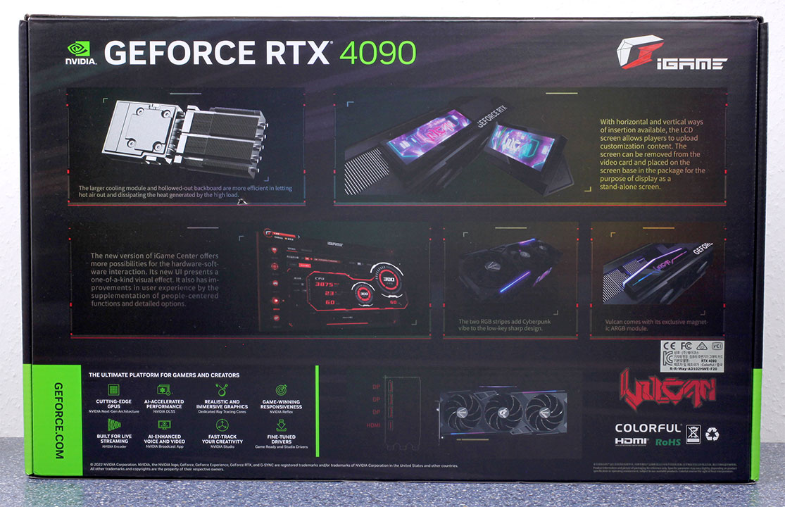
Packaging
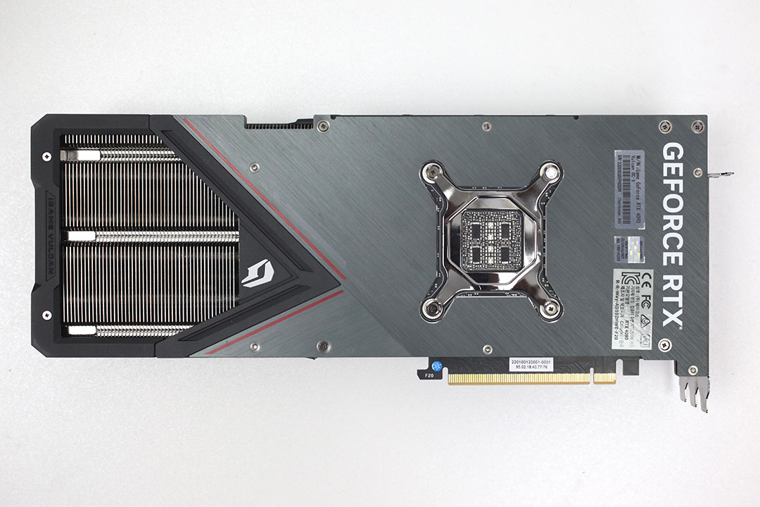
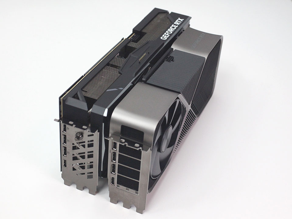
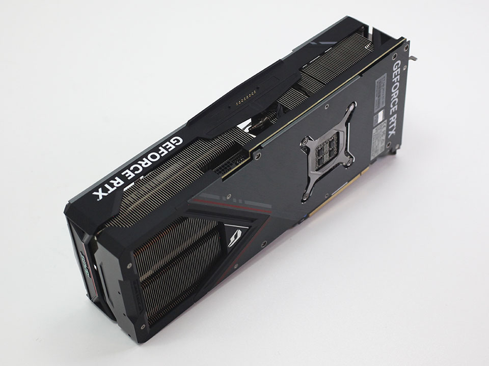
The Card
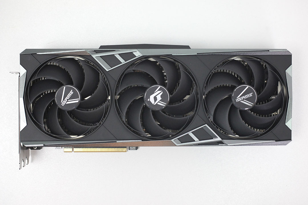
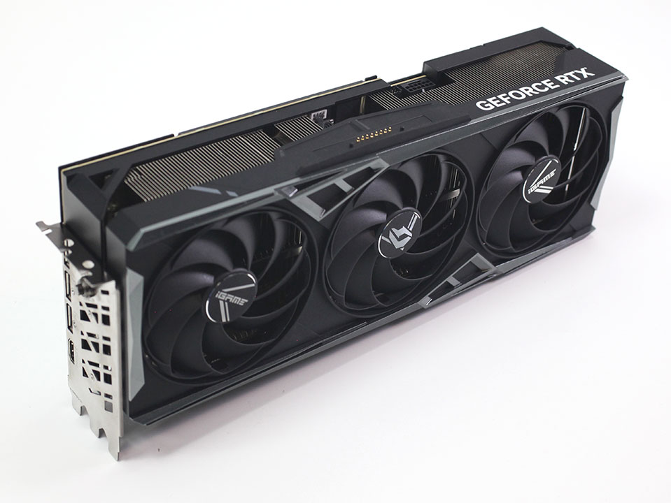
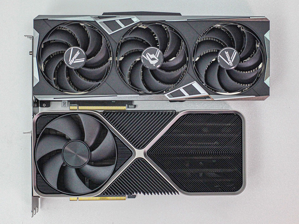
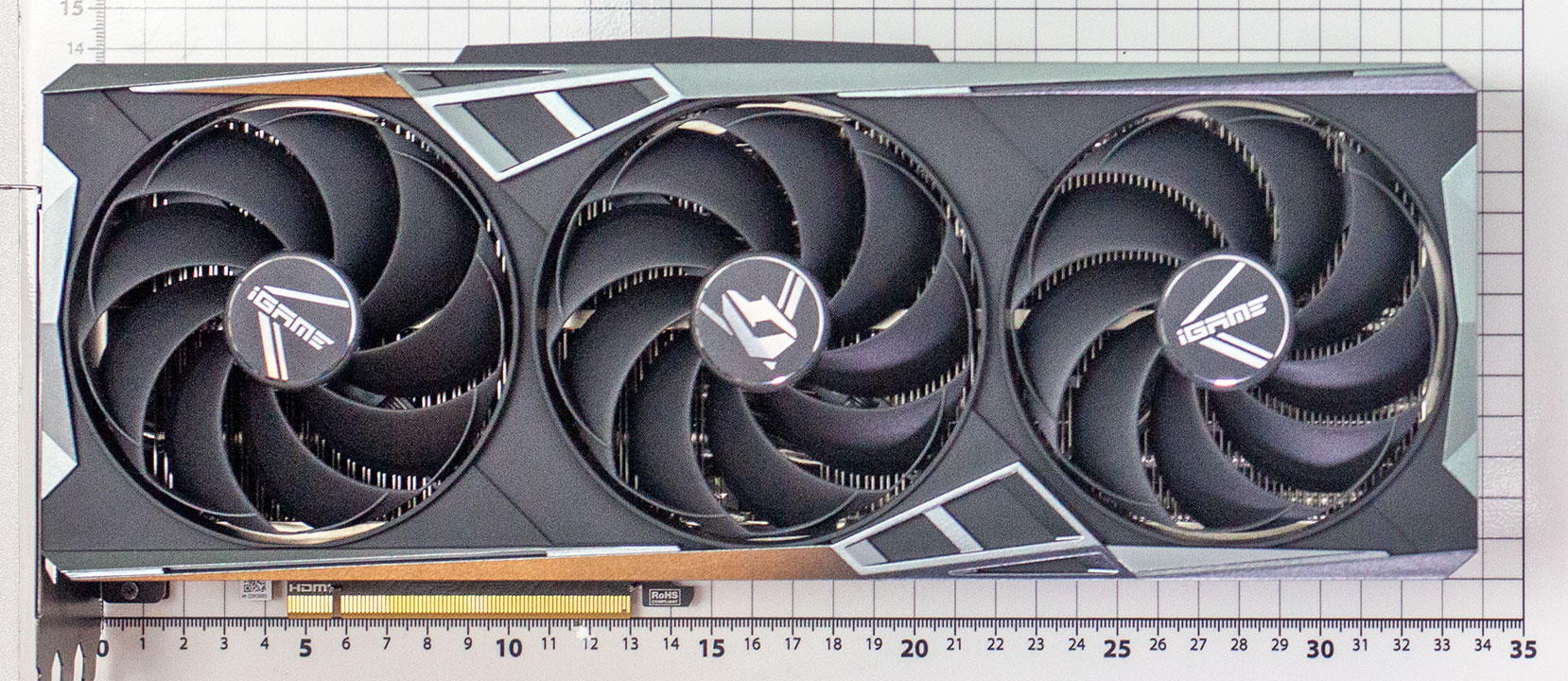
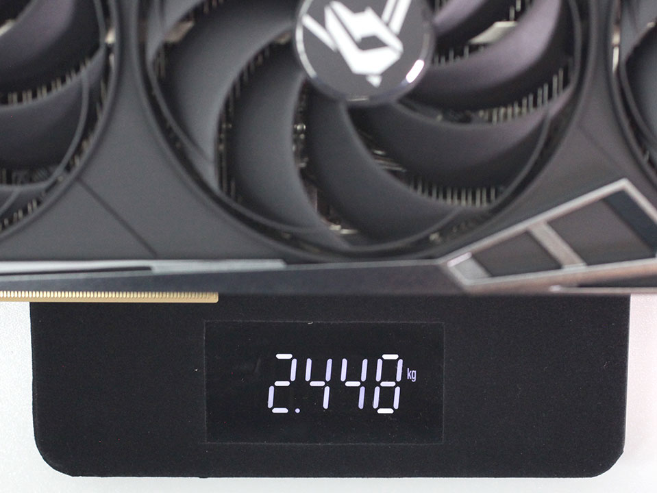
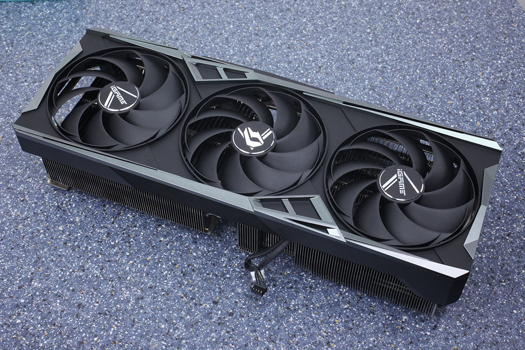
Dimensions of the card are 33.0 x 14.4 cm, and it weighs 2448 g.
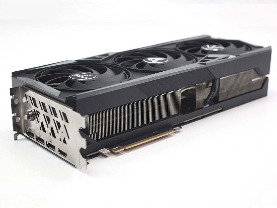
Installation requires four slots in your system.
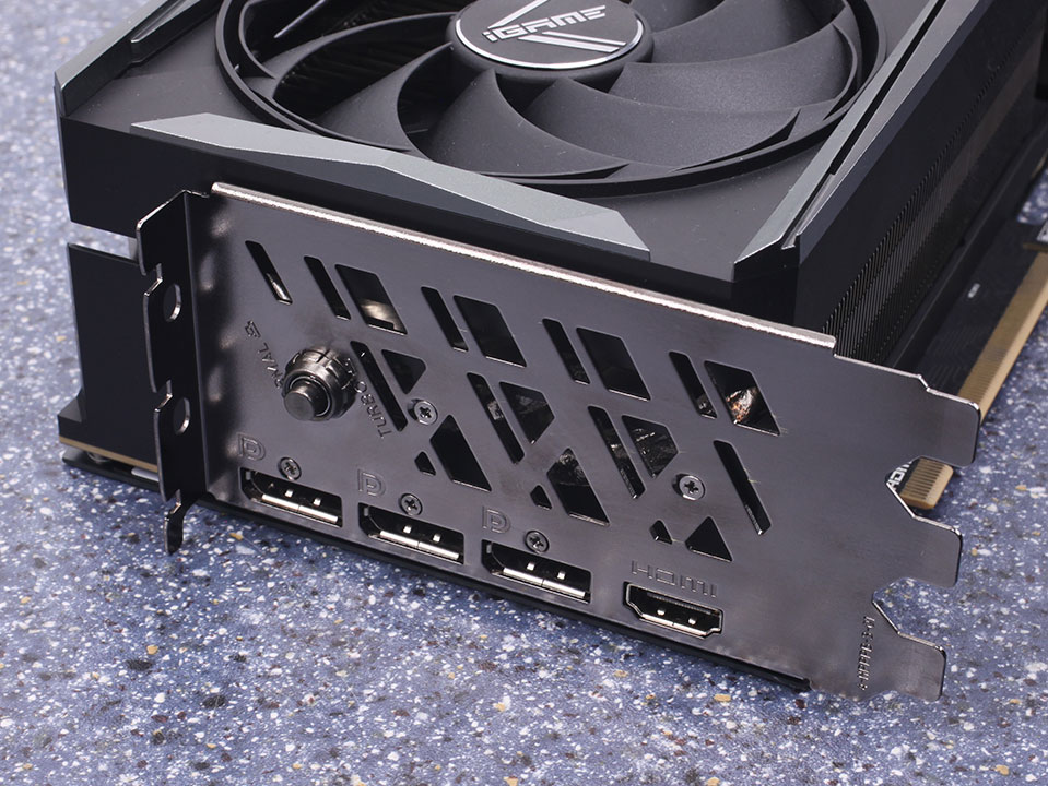
Display connectivity includes three standard DisplayPort 1.4a ports and one HDMI 2.1a (same as Ampere).
The button that you see on the slot cover is to switch from the default BIOS to a "turbo" BIOS, which runs at higher clocks and power limit.
NVIDIA introduced the concept of dual NVDEC and NVENC Codecs with the Ada architecture. This means there are two independent sets of hardware-accelerators; so you can encode and decode two streams of video in parallel or one stream at double the FPS rate. The new 8th Gen NVENC now accelerates AV1 encoding, besides HEVC. You also get an "optical flow accelerator" unit that is able to calculate intermediate frames for videos, to smooth playback. The same hardware unit is used for frame generation in DLSS 3.
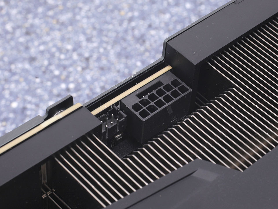
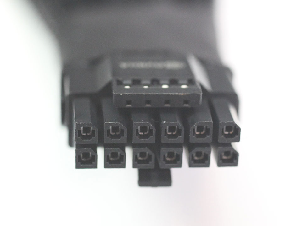
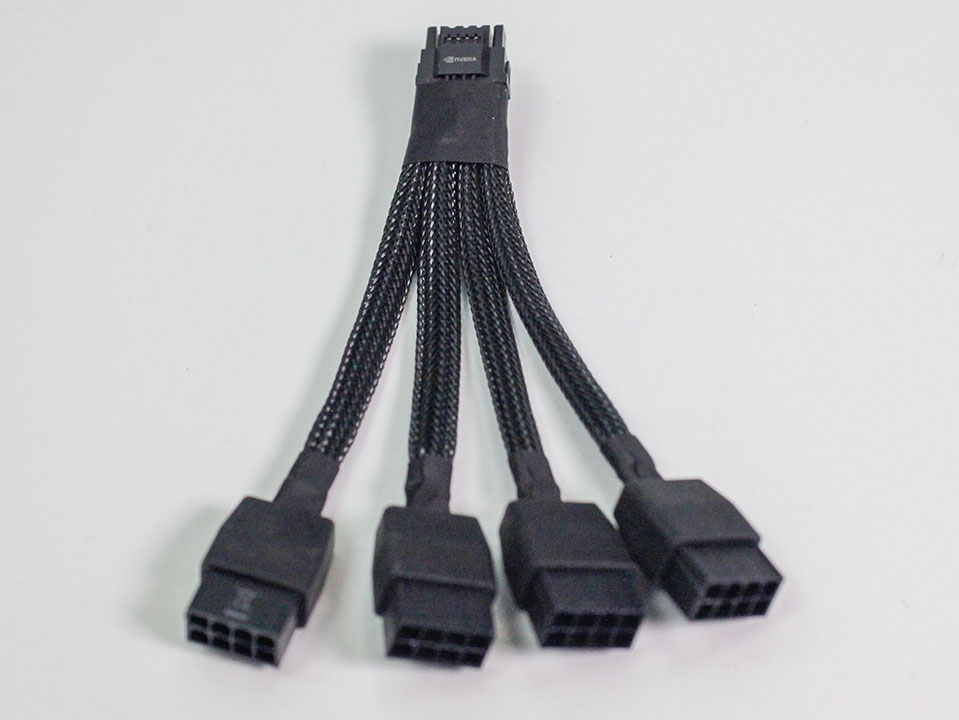
The card uses the new 12+4 pin ATX 12VHPWR connector, which is rated for up to 600 W of power draw. An adapter cable from 4x PCIe 8-pin is included, you can also run the card with just three 8-pins.
Teardown
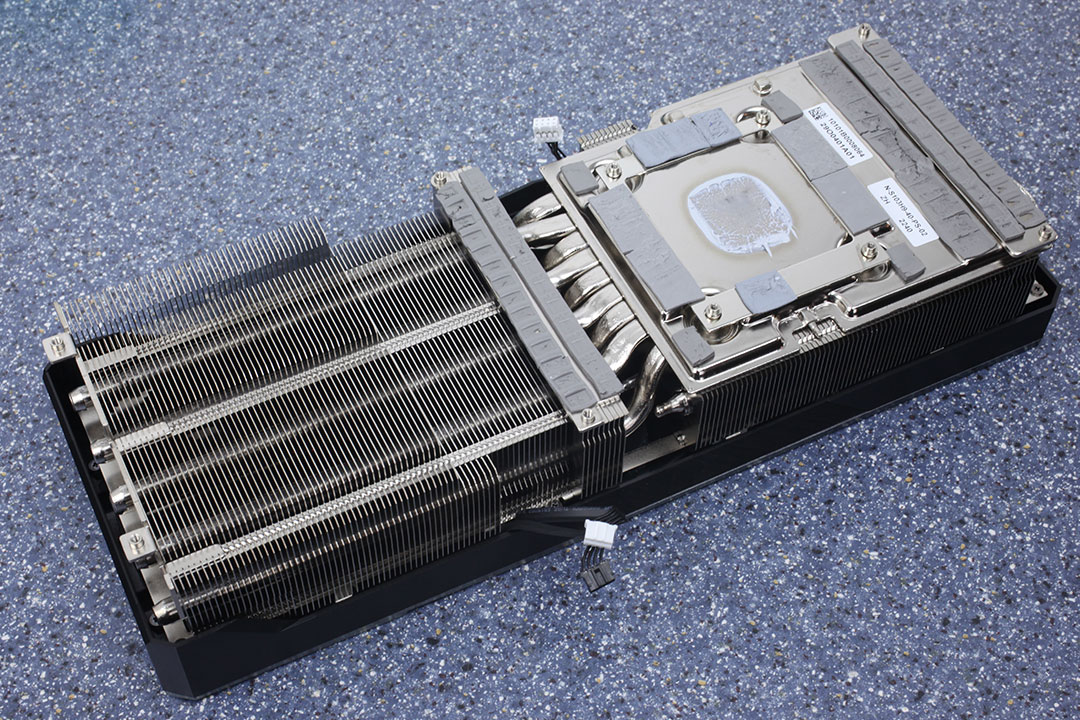
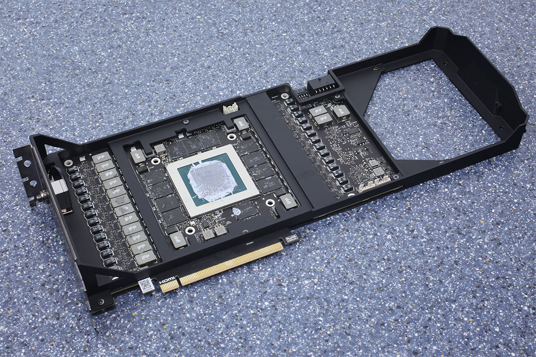
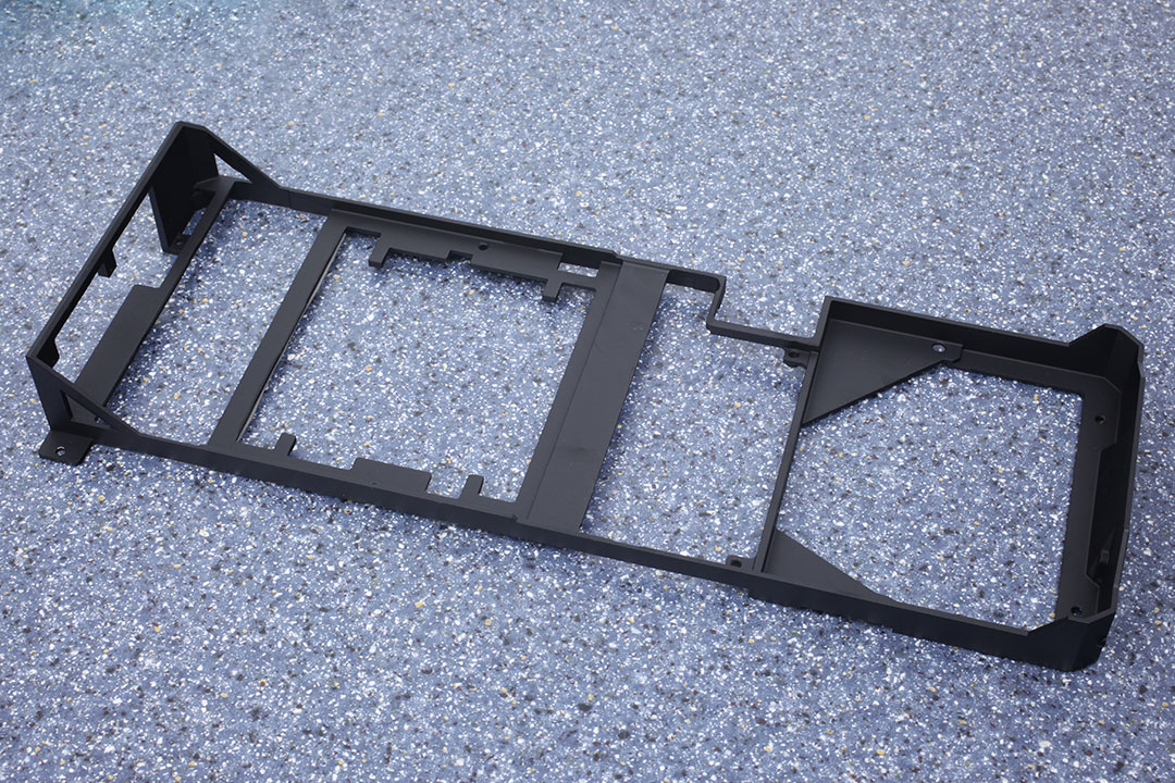
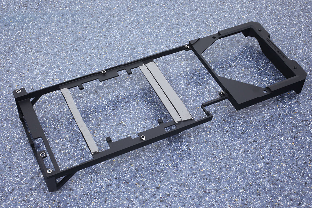
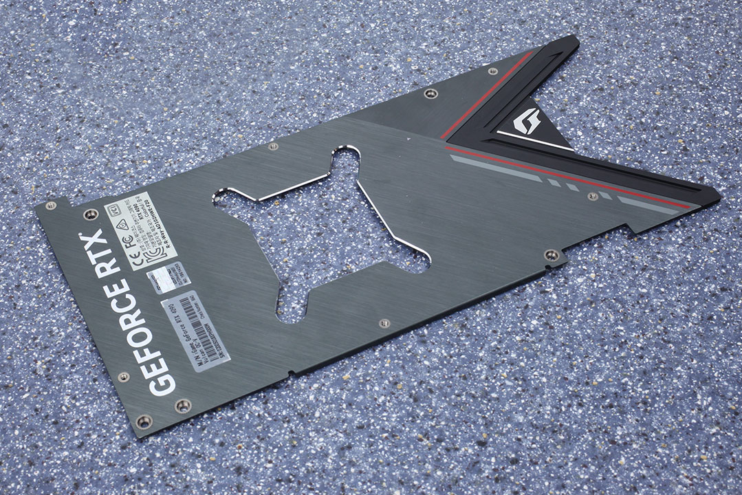
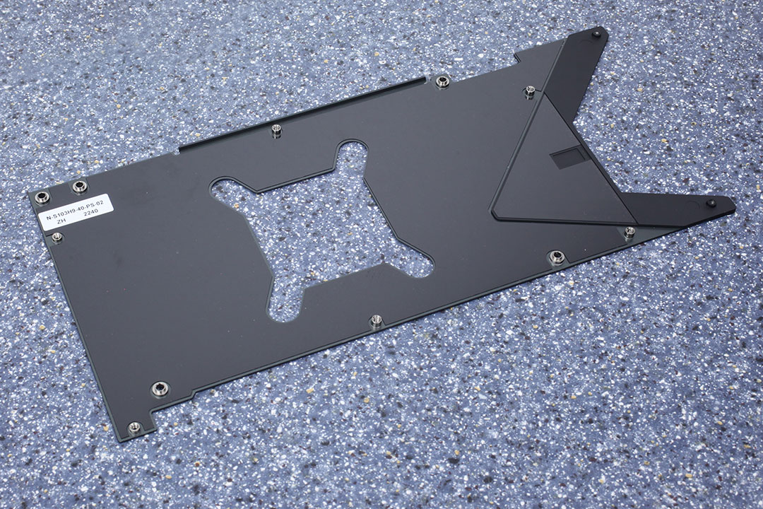
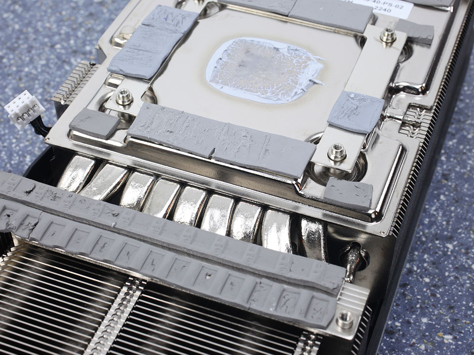
High-resolution PCB Pictures
These pictures are for the convenience of volt modders and people who would like to see all the finer details on the PCB. Feel free to link back to us and use these in your articles, videos or forum posts.

High-resolution versions are also available (front, back).
Our Patreon Silver Supporters can read articles in single-page format.
Apr 10th, 2025 03:21 EDT
change timezone
Latest GPU Drivers
New Forum Posts
- Do you use Linux? (570)
- [Update] FanControl (and other different monitoring software) blocked by Defender due to Winring0 vulnerability (1)
- Help with updating firmware on a AOC Agon Pro OLED monitor, says I need Install Tool (1)
- How is the Gainward Phoenix Model in terms of quality? (0)
- ## [Golden Sample] RTX 5080 – 3300 MHz @ 1.020 V (Stock Curve) – Ultra-Stable & Efficient (44)
- hp envy 15 rtx 2060 max-q stock vbios (1)
- Anyone know where to get driver updates / backdates for TUF A15? (0)
- (Some of) What I'd like to See From a Final Fantasy IX Remake (10)
- rtx 4060 ventus 8gb bios flash "HELP NEEDED!" (1)
- Downgrading bios on asrock A320 board (0)
Popular Reviews
- The Last Of Us Part 2 Performance Benchmark Review - 30 GPUs Compared
- ASRock Z890 Taichi OCF Review
- MCHOSE L7 Pro Review
- Sapphire Radeon RX 9070 XT Pulse Review
- PowerColor Radeon RX 9070 Hellhound Review
- Upcoming Hardware Launches 2025 (Updated Apr 2025)
- Sapphire Radeon RX 9070 XT Nitro+ Review - Beating NVIDIA
- Acer Predator GM9000 2 TB Review
- ASUS GeForce RTX 5080 Astral OC Review
- UPERFECT UStation Delta Max Review - Two Screens In One
Controversial News Posts
- NVIDIA GeForce RTX 5060 Ti 16 GB SKU Likely Launching at $499, According to Supply Chain Leak (173)
- MSI Doesn't Plan Radeon RX 9000 Series GPUs, Skips AMD RDNA 4 Generation Entirely (146)
- Microsoft Introduces Copilot for Gaming (124)
- AMD Radeon RX 9070 XT Reportedly Outperforms RTX 5080 Through Undervolting (119)
- NVIDIA Reportedly Prepares GeForce RTX 5060 and RTX 5060 Ti Unveil Tomorrow (115)
- Over 200,000 Sold Radeon RX 9070 and RX 9070 XT GPUs? AMD Says No Number was Given (100)
- Nintendo Confirms That Switch 2 Joy-Cons Will Not Utilize Hall Effect Stick Technology (99)
- Nintendo Switch 2 Launches June 5 at $449.99 with New Hardware and Games (99)