 8
8
Galax GeForce RTX 4070 Super EX Review
(8 Comments) »Introduction
Galax GeForce RTX 4070 Super EX is an affordable yet premium-looking custom-design graphics card based on NVIDIA's recently announced performance segment GPU. This card is also available with an identical name and model identifier, but under the KFA2 brand, in some markets. The GeForce RTX 4070 Super is part of a three-model refresh by NVIDIA this January, for the higher end of its GeForce RTX 40-series Ada family. It aims to improve the performance and competitiveness of the GeForce RTX brand at the $600 price-point that was previously held by the original RTX 4070, which had been embattled by AMD's recent introduction of the Radeon RX 7800 XT. The "Super" brand extension denotes an increase in performance at given price points without a change in the underlying technology. NVIDIA tends to roll these GPUs out one year into the lifecycle of a GPU generation.

The GeForce RTX 4070 Super continues to be based on the same 5 nm AD104 silicon powering the original RTX 4070 and RTX 4070 Ti, but is closer to the latter in specs, particularly with its shader count. The original RTX 4070 only enabled 46 out of 60 streaming multiprocessors (SM) present on the AD104, or just over three-quarters of it. The RTX 4070 Ti maxes out all 60 SMs, but was $800 at launch. The new RTX 4070 Super enables 56 out of 60 SM, or 93% of the available shaders. Compared to the original RTX 4070, this marks a neat 21% increase in CUDA cores, RT cores, Tensor cores, and TMUs. That's not all, the RTX 4070 Super gets all 48 MB of L2 cache available on the AD104 silicon, the original RTX 4070 only has 36 MB of it; and there's even an increase in the ROP count—the RTX 4070 only had 64 out of 80 ROPs enabled; while the RTX 4070 Super, like the RTX 4070 Ti, has all 80 of them enabled.
With 56 SMs on tap, the GeForce RTX 4070 Super enjoys 7,168 CUDA cores, 224 Tensor cores, 56 RT cores, 224 TMUs, and 80 ROPs, besides all 48 MB of L2 cache. The memory sub-system is carried over from the original, you get 12 GB of GDDR6X memory across a 192-bit memory interface, running at 21 Gbps, for 504 GB/s of memory bandwidth on tap. The increased shader counts, and slightly higher GPU clocks have meant that NVIDIA has had to increase the total graphics power (TGP) of the RTX 4070 Super, to 220 W, up from 200 W for the RTX 4070; but which is still less than the lavish 285 W enjoyed by the RTX 4070 Ti. Even this bit of increase has meant that NVIDIA's board partners can no longer opt for a single 8-pin PCIe power connector configuration, and all cards, including the Galax we're reviewing today, come with a 16-pin 12VHPWR power connector, and an NVIDIA-designed adapter that converts two 8-pin PCIe to a 300 W-rated 12VHPWR.
As we mentioned before, the underlying Ada graphics architecture is unchanged. Designed to take advantage of the 5 nm EUV foundry node, Ada introduces a new generation CUDA core with increased IPC, and support for shader-execution reordering, which improves ray tracing performance; the new 3rd generation RT core that supports displaced micro-meshes that allow game designers to increase complexity of ray traced objects; and the new optical flow accelerator component, which enables DLSS 3 Frame Generation, a path-breaking feature that lets the GPU draw entire alternate frames using AI, without involving the main graphics rendering machinery. NVIDIA has also re-architected the memory sub-system for this generation, by placing a nearly 10-times larger fast on-die L2 cache on the GPU, which reduces round-trips to the video memory by a significant enough amount to allow NVIDIA to narrow down the memory bus to 192-bit (compared to something like the previous-gen RTX 3070 Ti, which enjoyed 256-bit). This narrower memory bus drives memory chips of generationally increased density, which is how the card has 12 GB.
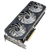
The Galax RTX 4070 Super EX sports a premium appearance, with a triple-slot design, and cooler that looks like it's from a segment above. It uses an aluminium fin-stack heatsink with three heatpipes; and a trio of fans. The one in the middle is slightly larger 102 mm than the ones on the sides, at 92 mm, each. The three fans, along with a GeForce RTX logo on the topside of the cooler shroud, are RGB LED illuminated, and you can control it using the Galax Xtreme Tuner app. The card has its own RGB controller; but also puts out a 3-pin addressable RGB header, so you can sync the rest of your lighting to the card. The Galax EX comes with a handy factory overclock of 2565 MHz out of the box, compared to 2475 MHz reference. The card is priced at $615, an acceptable $15 premium over the NVIDIA baseline price.
| Price | Cores | ROPs | Core Clock | Boost Clock | Memory Clock | GPU | Transistors | Memory | |
|---|---|---|---|---|---|---|---|---|---|
| RTX 4060 Ti | $390 | 4352 | 48 | 2310 MHz | 2535 MHz | 2250 MHz | AD106 | 22900M | 8 GB, GDDR6, 128-bit |
| RX 6700 XT | $300 | 2560 | 64 | 2424 MHz | 2581 MHz | 2000 MHz | Navi 22 | 17200M | 12 GB, GDDR6, 192-bit |
| RTX 3070 | $310 | 5888 | 96 | 1500 MHz | 1725 MHz | 1750 MHz | GA104 | 17400M | 8 GB, GDDR6, 256-bit |
| RTX 3070 Ti | $350 | 6144 | 96 | 1575 MHz | 1770 MHz | 1188 MHz | GA104 | 17400M | 8 GB, GDDR6X, 256-bit |
| RX 6800 | $450 | 3840 | 96 | 1815 MHz | 2105 MHz | 2000 MHz | Navi 21 | 26800M | 16 GB, GDDR6, 256-bit |
| RX 7700 XT | $430 | 3456 | 96 | 2171 MHz | 2544 MHz | 2250 MHz | Navi 32 | 26500M | 12 GB, GDDR6, 192-bit |
| RX 6800 XT | $500 | 4608 | 128 | 2015 MHz | 2250 MHz | 2000 MHz | Navi 21 | 26800M | 16 GB, GDDR6, 256-bit |
| RTX 3080 | $450 | 8704 | 96 | 1440 MHz | 1710 MHz | 1188 MHz | GA102 | 28000M | 10 GB, GDDR6X, 320-bit |
| RTX 4070 | $540 | 5888 | 64 | 1920 MHz | 2475 MHz | 1313 MHz | AD104 | 35800M | 12 GB, GDDR6X, 192-bit |
| RX 7800 XT | $510 | 3840 | 96 | 2124 MHz | 2430 MHz | 2425 MHz | Navi 32 | 28100M | 16 GB, GDDR6, 256-bit |
| RX 6900 XT | $650 | 5120 | 128 | 2015 MHz | 2250 MHz | 2000 MHz | Navi 21 | 26800M | 16 GB, GDDR6, 256-bit |
| RX 6950 XT | $630 | 5120 | 128 | 2100 MHz | 2310 MHz | 2250 MHz | Navi 21 | 26800M | 16 GB, GDDR6, 256-bit |
| RTX 3090 | $800 | 10496 | 112 | 1395 MHz | 1695 MHz | 1219 MHz | GA102 | 28000M | 24 GB, GDDR6X, 384-bit |
| RTX 4070 Super | $590 | 7168 | 80 | 1980 MHz | 2475 MHz | 1313 MHz | AD104 | 35800M | 12 GB, GDDR6X, 192-bit |
| Galax RTX 4070 Super EX | $615 | 7168 | 80 | 1980 MHz | 2565 MHz | 1313 MHz | AD104 | 35800M | 12 GB, GDDR6X, 192-bit |
| RX 7900 GRE | $550 | 5120 | 160 | 1880 MHz | 2245 MHz | 2250 MHz | Navi 31 | 57700M | 16 GB, GDDR6, 256-bit |
| RTX 4070 Ti | $750 | 7680 | 80 | 2310 MHz | 2610 MHz | 1313 MHz | AD104 | 35800M | 12 GB, GDDR6X, 192-bit |
| RTX 4070 Ti Super | $800 | 8448 | 96 | 2340 MHz | 2610 MHz | 1313 MHz | AD103 | 45900M | 16 GB, GDDR6X, 256-bit |
| RX 7900 XT | $760 | 5376 | 192 | 2000 MHz | 2400 MHz | 2500 MHz | Navi 31 | 57700M | 20 GB, GDDR6, 320-bit |
| RTX 3090 Ti | $1050 | 10752 | 112 | 1560 MHz | 1950 MHz | 1313 MHz | GA102 | 28000M | 24 GB, GDDR6X, 384-bit |
| RTX 4080 | $1200 | 9728 | 112 | 2205 MHz | 2505 MHz | 1400 MHz | AD103 | 45900M | 16 GB, GDDR6X, 256-bit |
| RTX 4080 Super | $1000 | 10240 | 112 | 2295 MHz | 2550 MHz | 1438 MHz | AD103 | 45900M | 16 GB, GDDR6X, 256-bit |
Packaging


The Card


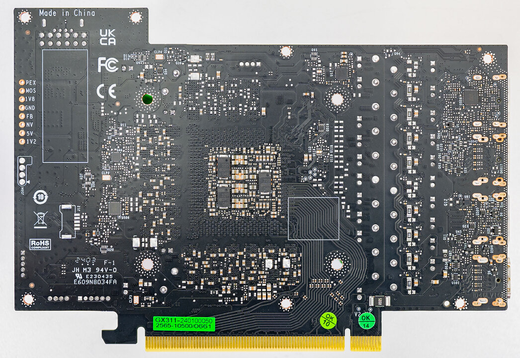
The Galax RTX 4070 Super EX comes with a black color theme, the backplate has some white highlights. There's a cutout for air to flow through, and the main cooler shroud is made from plastic while the backplate is made of metal.


Dimensions of the card are 32 x 13 cm, and it weighs 1065 g.


Installation requires three slots in your system. We measured the card's width to be 50 mm.

Display connectivity includes three standard DisplayPort 1.4a ports and one HDMI 2.1a (same as Ampere and same as non-Super Ada).
NVIDIA introduced the concept of dual NVDEC and NVENC Codecs with the Ada Lovelace architecture. This means there are two independent sets of hardware-accelerators; so you can encode and decode two streams of video in parallel or one stream at double the FPS rate. While the RTX 4070 Ti features dual units, the RTX 4070 Super and RTX 4070 come with only one of them. The new 8th Gen NVENC now accelerates AV1 encoding, besides HEVC. You also get an "optical flow accelerator" unit that is able to calculate intermediate frames for videos, to smooth playback. The same hardware unit is used for frame generation in DLSS 3.

All GeForce RTX 4070 Super graphics cards use the 12+4 pin ATX 12VHPWR connector, an adapter cable is included in the box.
Teardown


The thermal solution on the Galax EX has three heatpipes. The main heatsink also provides cooling for the memory chips and VRM circuitry.


The backplate is made of metal and protects the card against damage during installation and handling.
High-resolution PCB Pictures
These pictures are for the convenience of volt modders and people who would like to see all the finer details on the PCB. Feel free to link back to us and use these in your articles, videos or forum posts.
High-resolution versions are also available (front, back).
Circuit Board (PCB) Analysis


GPU voltage is an eight-phase design, managed by a uPI uP9512R controller.

The GPU VRM uses AOZ5311NQI DrMOS components by Alpha & Omega Semiconductor, rated for 55 A.

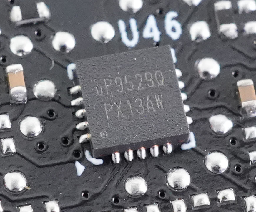
Memory voltage is a two-phase design, managed by a uPI uP9529Q controller.

For memory, AOZ5311NQI DrMOS with a 50 A rating are used, too.

The GDDR6X memory chips are made by Micron and carry the model number D8BZC, which decodes to MT61K512M32KPA-21:U. They are specified to run at 1313 MHz (21 Gbps GDDR6 effective).
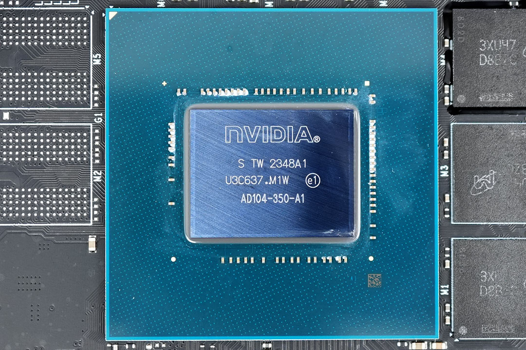
NVIDIA's AD104 graphics processor is the company's third Ada Lovelace GPU. It is built using a 5 nanometer process at TSMC Taiwan, with a transistor count of 35.8 billion and a die size of 295 mm².
Test System
| Test System - GPU 2024.1 | |
|---|---|
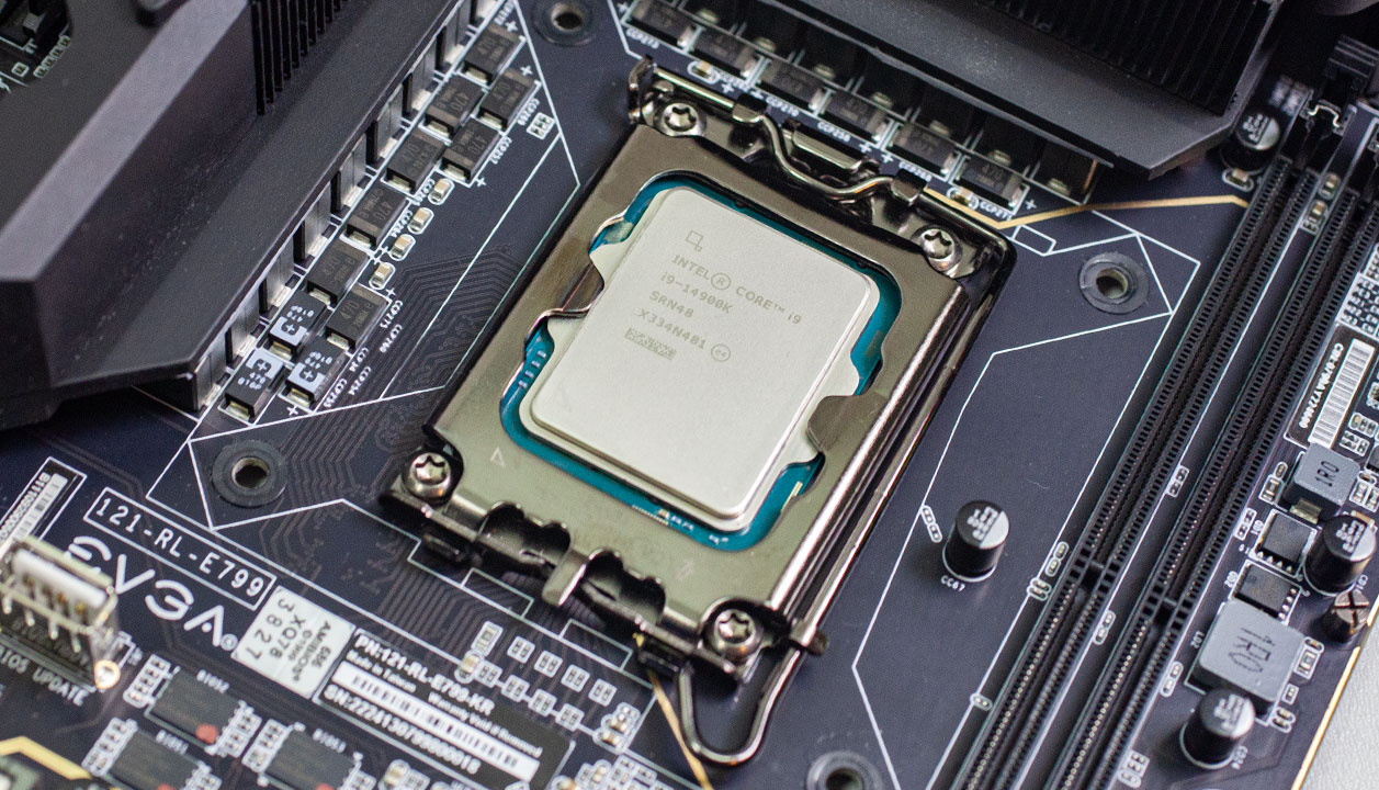
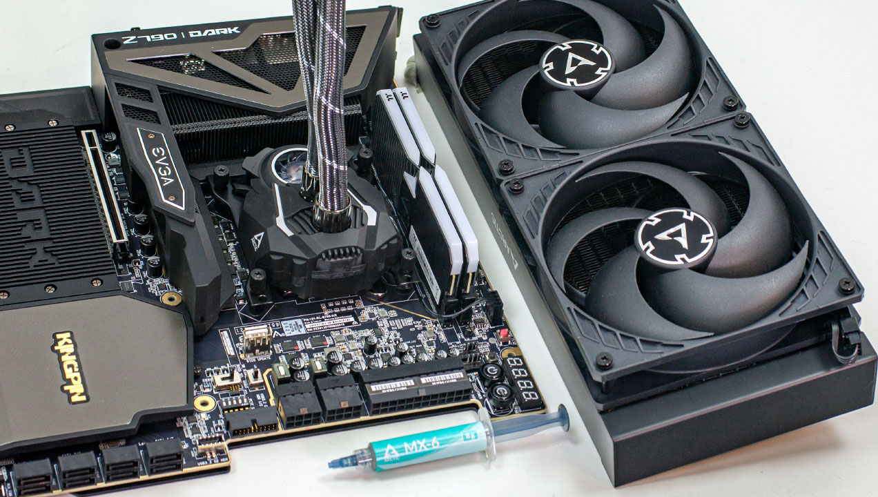
| Processor: | Intel Core i9-14900K Raptor Lake, 6.0 GHz, 8+16 cores / 32 threads PL1 = PL2 = 330 W |
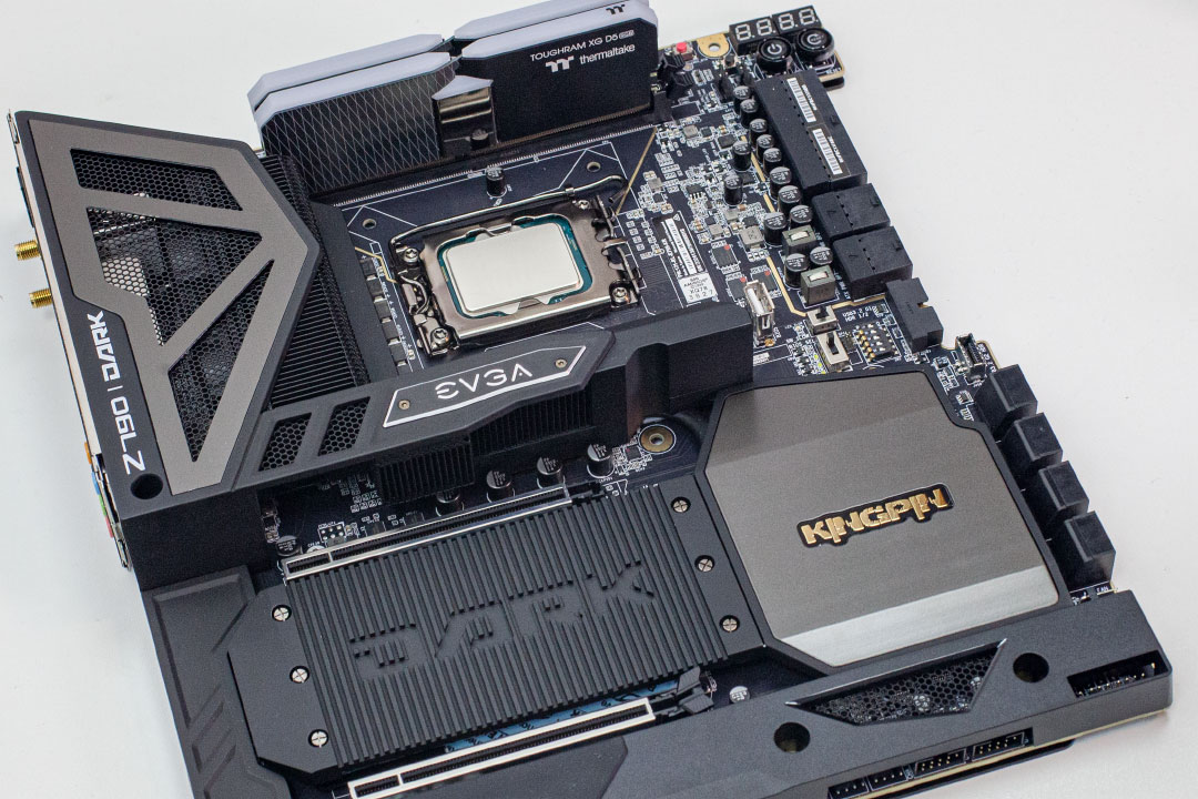
| Motherboard: | EVGA Z790 Dark BIOS 1.13 |
| Resizable BAR: | Enabled on all supported cards (NVIDIA, AMD & Intel) |
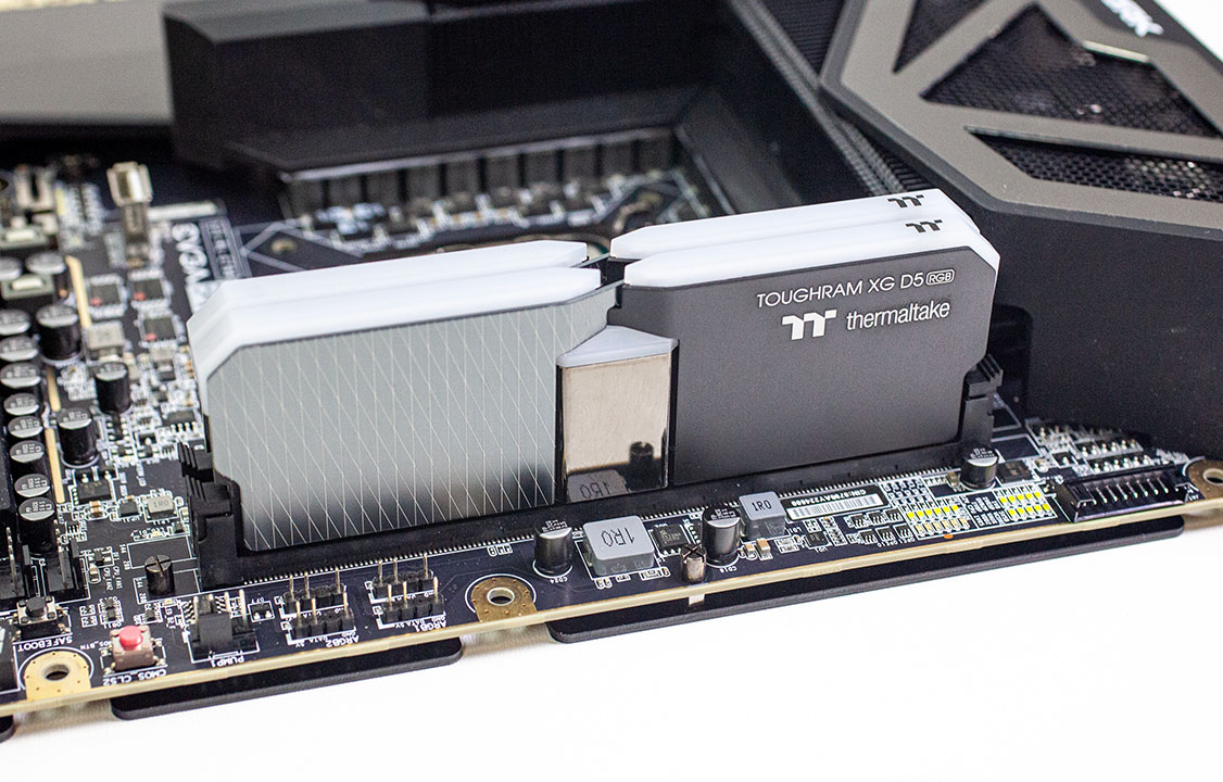
| Memory: | Thermaltake TOUGHRAM XG 2x 16 GB DDR5-7200 MHz 36-46-46-96 |
| Cooling: | Arctic Liquid Freezer II 280 mm AIO |
| Thermal Paste: | Arctic MX-6 |
| Storage: | 2x 2 TB M.2 NVMe SSD |
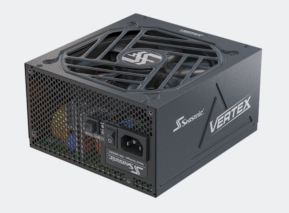
| Power Supply: | Seasonic Vertex GX 850 W ATX 3.0 / 16-pin 12VHPWR |
| Case: | darkFlash DLX4000 Mesh |
| Operating System: | Windows 11 Professional 64-bit 23H2 VBS enabled (Windows 11 default) |
| Drivers: | RX 7900 GRE: 23.40.19.01 Press Driver RTX 3050 6 GB: 551.23 WHQL RTX 4080 Super: 551.22 Press Driver RTX 4070 Super & 4070 Ti Super: 551.23 WHQL NVIDIA: 546.17 WHQL AMD: 23.11.1 WHQL Intel: 101.4953 WHQL Date of Retest |
- All games and cards are tested with the drivers listed above—no performance results were recycled between test systems. Only this exact system with exactly the same configuration is used for all results in this review.
- All graphics cards are tested using the same game version.
- All games are set to their highest quality setting unless indicated otherwise.
- AA and AF are applied via in-game settings, not via the driver's control panel.
- Before starting measurements, we heat up the card for each test to ensure a steady state is tested. This ensures that the card won't boost to unrealistically high clocks for only a few seconds until it heats up, as that doesn't represent prolonged gameplay.
- For better real-life applicability, all game tests use custom in-game test scenes, not the integrated benchmarks
- All cards used for comparison are reference designs. When a reference design does not exist, we go the extra mile and buy the closest possible match, using reference clocks and default power limit.
- 1920x1080: Most popular monitor resolution.
- 2560x1440: Intermediary resolution between Full HD and 4K, with reasonable performance requirements.
- 3840x2160: 4K Ultra HD resolution, available on high-end monitors.
Our Patreon Silver Supporters can read articles in single-page format.
May 5th, 2025 03:43 EDT
change timezone
Latest GPU Drivers
New Forum Posts
- Choosing an Internal HDD (61)
- Asus motherboard AM5 safe to buy in 2025? (15)
- Low budget psu for medium high loads (under 400 watt usage) (21)
- Post your Speedtest.net Speeds! (2360)
- It's happening again, melting 12v high pwr connectors (1053)
- Are the 8 GB cards worth it? (860)
- [AV1, AV2, AV3 codecs...] Have they given up on the AOMedia project? (15)
- RX 9000 series GPU Owners Club (639)
- I got a new motherboard about to start a DTS journey (2)
- Windows 11 General Discussion (6023)
Popular Reviews
- ASUS ROG Maximus Z890 Hero Review
- ASUS Radeon RX 9070 XT TUF OC Review
- Clair Obscur: Expedition 33 Performance Benchmark Review - 33 GPUs Tested
- Montech HS02 PRO Review
- NVIDIA GeForce RTX 5060 Ti 8 GB Review - So Many Compromises
- Seasonic Vertex GX 850 W Review
- Upcoming Hardware Launches 2025 (Updated Apr 2025)
- ASUS GeForce RTX 5090 Astral Liquid OC Review - The Most Expensive GPU I've Ever Tested
- Sapphire Radeon RX 9070 XT Nitro+ Review - Beating NVIDIA
- AMD Ryzen 7 9800X3D Review - The Best Gaming Processor
Controversial News Posts
- AMD Radeon RX 9060 XT to Roll Out 8 GB GDDR6 Edition, Despite Rumors (129)
- NVIDIA Sends MSRP Numbers to Partners: GeForce RTX 5060 Ti 8 GB at $379, RTX 5060 Ti 16 GB at $429 (128)
- NVIDIA Launches GeForce RTX 5060 Series, Beginning with RTX 5060 Ti This Week (115)
- Nintendo Confirms That Switch 2 Joy-Cons Will Not Utilize Hall Effect Stick Technology (105)
- NVIDIA PhysX and Flow Made Fully Open-Source (95)
- Sony Increases the PS5 Pricing in EMEA and ANZ by Around 25 Percent (84)
- Parts of NVIDIA GeForce RTX 50 Series GPU PCB Reach Over 100°C: Report (78)
- Intel "Bartlett Lake-S" Gaming CPU is Possible, More Hints Appear for a 12 P-Core SKU (77)