 22
22
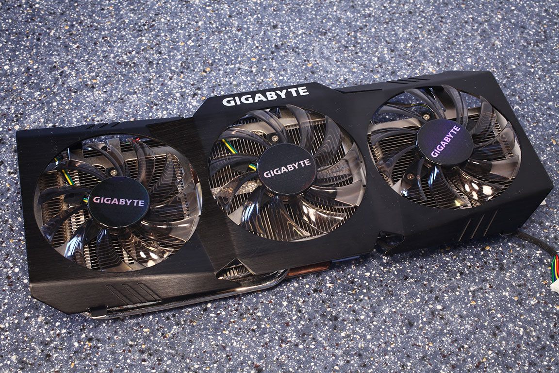
GIGABYTE GTX 480 GV-N480SO-15I Super Overclock Review
Test Setup »A Closer Look
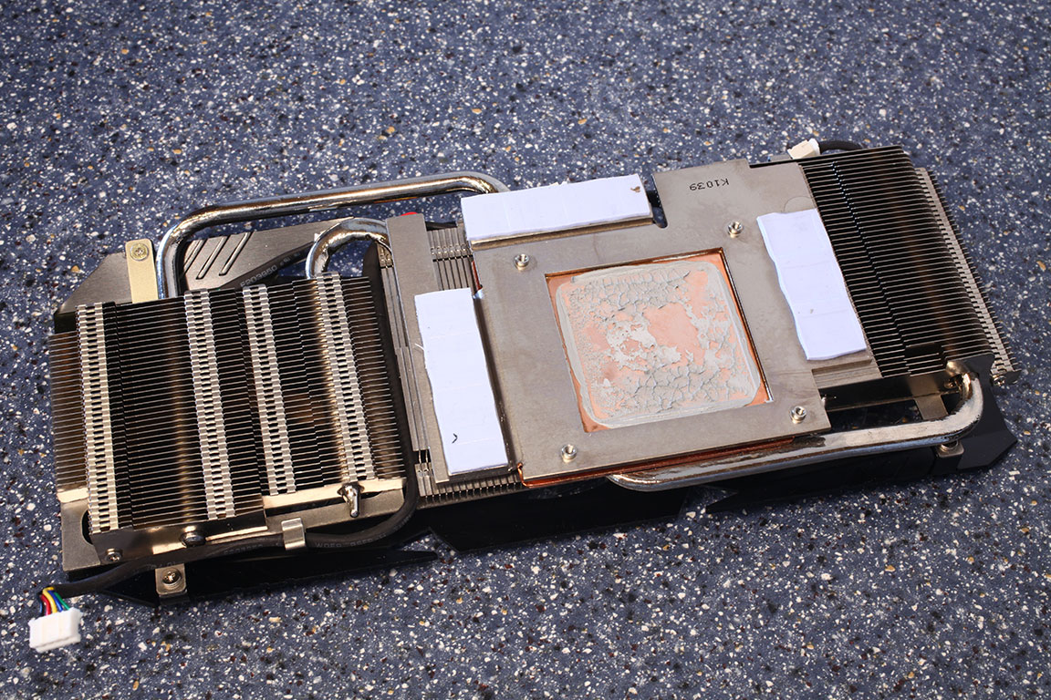
Gigabyte uses a Vapor Chamber heatsink base to transport heat away quickly from the GPU core to the heatsink. You can also see the thermal pads that keep the memory and VRM circuitry cool.

The 6+8 power input configuration is specified up to 300 W maximum power draw. It would have been nice to see a more beefy configuration here to provide plenty of power for hardcore overclockers. On the other hand, this power configuration will have no problems when the other components in the system are designed for overclocking and of high quality.
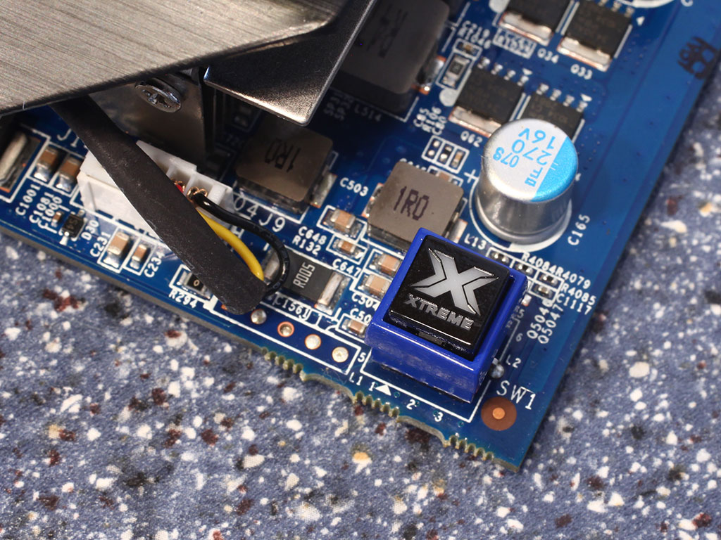
This little switch near the edge of the PCB lets you toggle between the normal BIOS and a BIOS especially optimized for LN2 usage. This means that there is no coldbug present, for example. Unfortunately the switch is quite difficult to reach when the card is installed in-case, it should be no problem on an open bench.
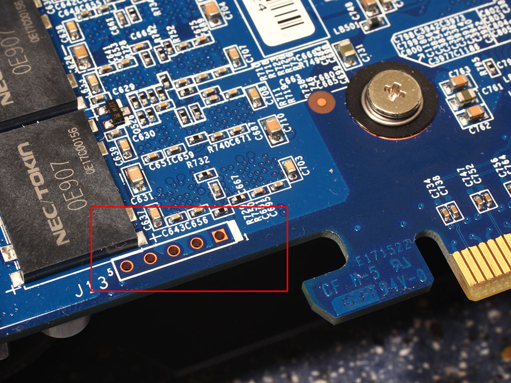
Gigabyte has included voltage measurement points for the most important GPU voltages on their card. But those measure points are in a horrible location that is almost impossible to get your measurement probes to, even on an open bench. You always have the possibility to solder your own test leads to the solder pads, but I'd prefer a non-permanent solution.
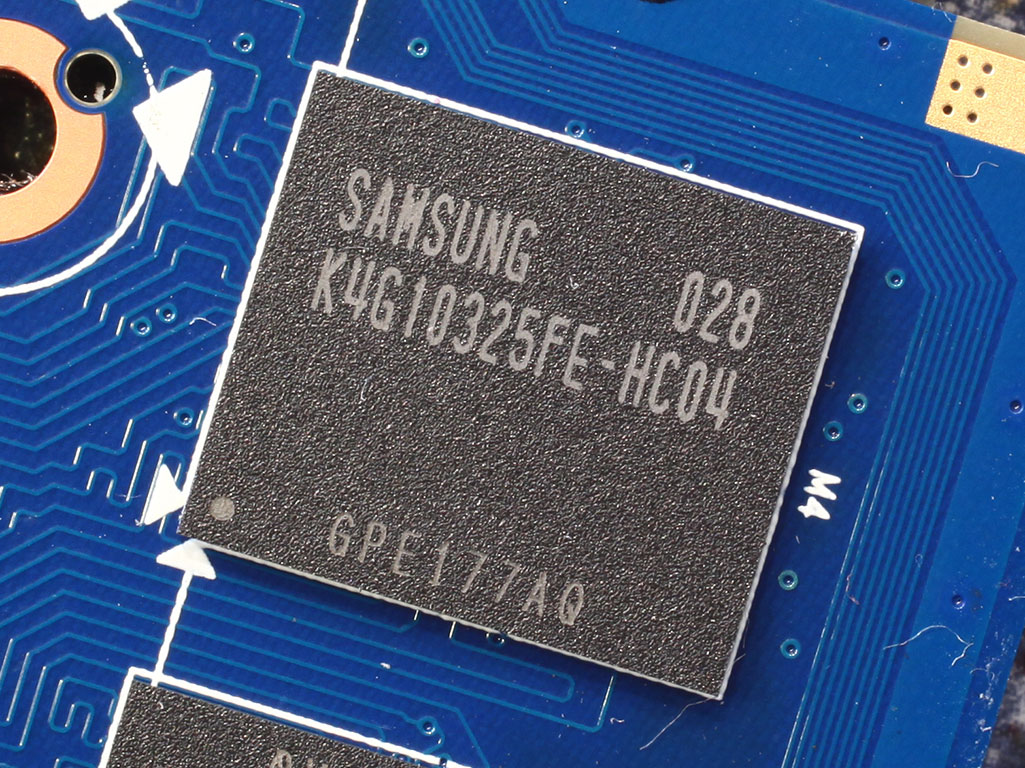
The GDDR5 memory chips are made by Samsung, and carry the model number K4G10325FE-HC04. They are specified to run at 1250 MHz (5000 MHz GDDR5 effective).
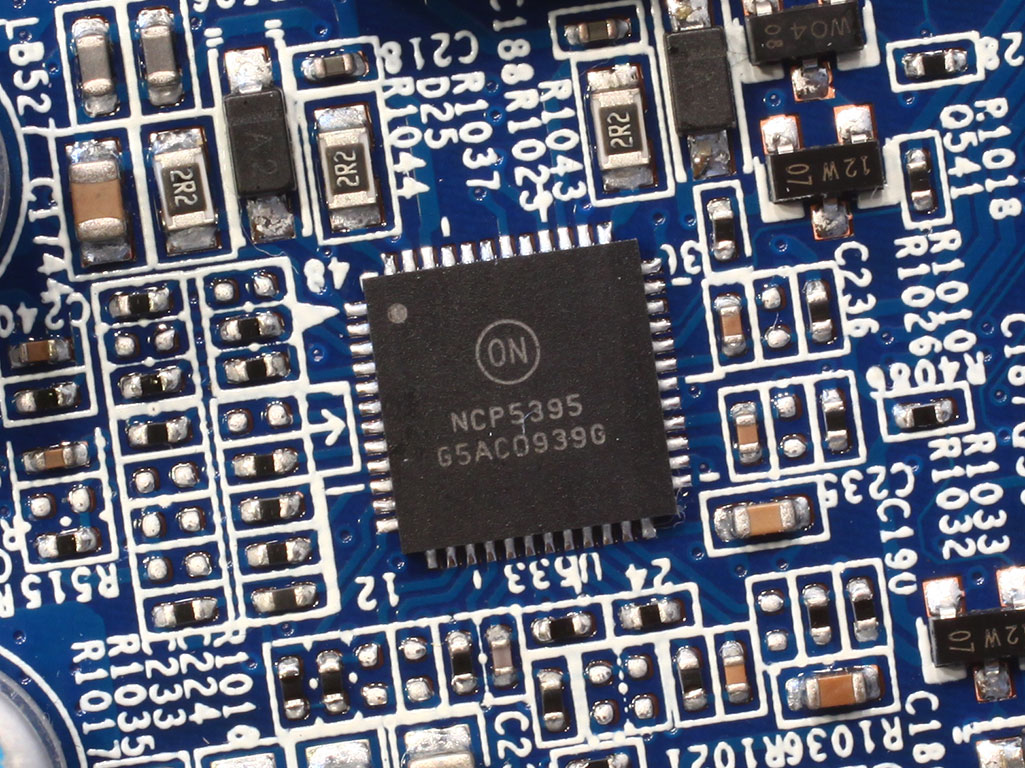
Gigabyte has chosen an NCP5395 as voltage regulator. Compared to the CHiL solution of the reference design, the NCP5395 is less capable, but Gigabyte has paired it with another chip to enhance voltage control and monitoring. Overall the solution seems decent but works only well when used with Gigabyte's own overclocking software.
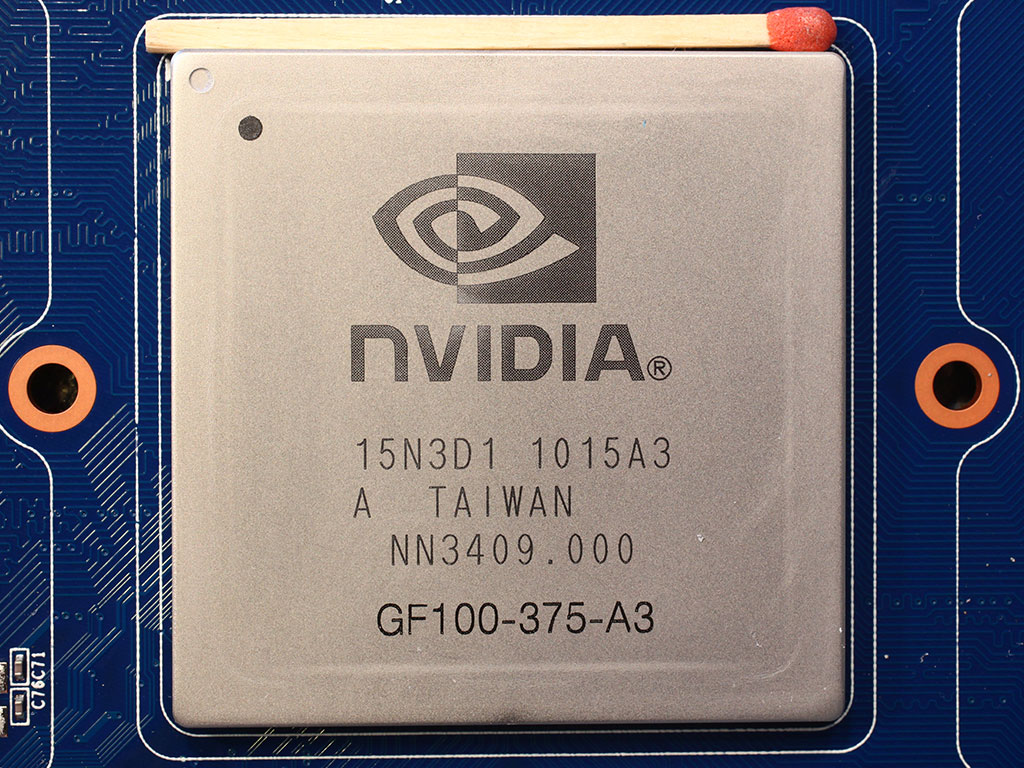
NVIDIA's GF100 graphics processor is made on a 40 nm process at TSMC Taiwan. It uses approximately 3.2 billion transistors which makes it the most complex GPU built to-date. Please note that the silvery metal surface you see is the heatspreader of the GPU which measures 42.3 x 42.3 mm. The actual GPU die is sitting under the heatspreader, and roughly 526 mm² in size.
Feb 25th, 2025 08:45 EST
change timezone
Latest GPU Drivers
New Forum Posts
- Free Games Thread (4487)
- Nvidia's GPU market share hits 90% in Q4 2024 (gets closer to full monopoly) (599)
- Microcenter GPU Stock status (13)
- 572.42 Drivers, Screen Blacking Out? (22)
- Authenticode fails for GPU-Z 2.63.0 (4)
- What's your latest tech purchase? (23207)
- Solidigm NVMe Custom Modded Driver for All NVMe Brands SSDs & Any NVMe SSDs (211)
- Cs2 Freezing in Rx 580 (7)
- Zotac RTX 3060Ti Twin Edge OC LHR PCB image (4)
- Freesync + Borderless Windowed Mode Stuttering (0)
Popular Reviews
- ASUS GeForce RTX 5070 Ti TUF OC Review
- MSI GeForce RTX 5070 Ti Vanguard SOC Review
- MSI GeForce RTX 5070 Ti Ventus 3X OC Review
- Corsair Xeneon 34WQHD240-C Review - Pretty In White
- MSI GeForce RTX 5070 Ti Gaming Trio OC+ Review
- Corsair Virtuoso MAX Wireless Review
- darkFlash DY470 Review
- Palit GeForce RTX 5070 Ti GameRock OC Review
- AMD Ryzen 7 9800X3D Review - The Best Gaming Processor
- Gigabyte GeForce RTX 5090 Gaming OC Review
Controversial News Posts
- NVIDIA GeForce RTX 50 Cards Spotted with Missing ROPs, NVIDIA Confirms the Issue, Multiple Vendors Affected (484)
- AMD Radeon 9070 XT Rumored to Outpace RTX 5070 Ti by Almost 15% (304)
- AMD Plans Aggressive Price Competition with Radeon RX 9000 Series (272)
- AMD Radeon RX 9070 and 9070 XT Listed On Amazon - One Buyer Snags a Unit (247)
- Edward Snowden Lashes Out at NVIDIA Over GeForce RTX 50 Pricing And Value (241)
- NVIDIA Investigates GeForce RTX 50 Series "Blackwell" Black Screen and BSOD Issues (240)
- AMD Denies Radeon RX 9070 XT $899 USD Starting Price Point Rumors (239)
- AMD Radeon RX 9070 and 9070 XT Official Performance Metrics Leaked, +42% 4K Performance Over Radeon RX 7900 GRE (168)