 508
508
Intel Core Ultra 9 285K Review
(508 Comments) »Introduction
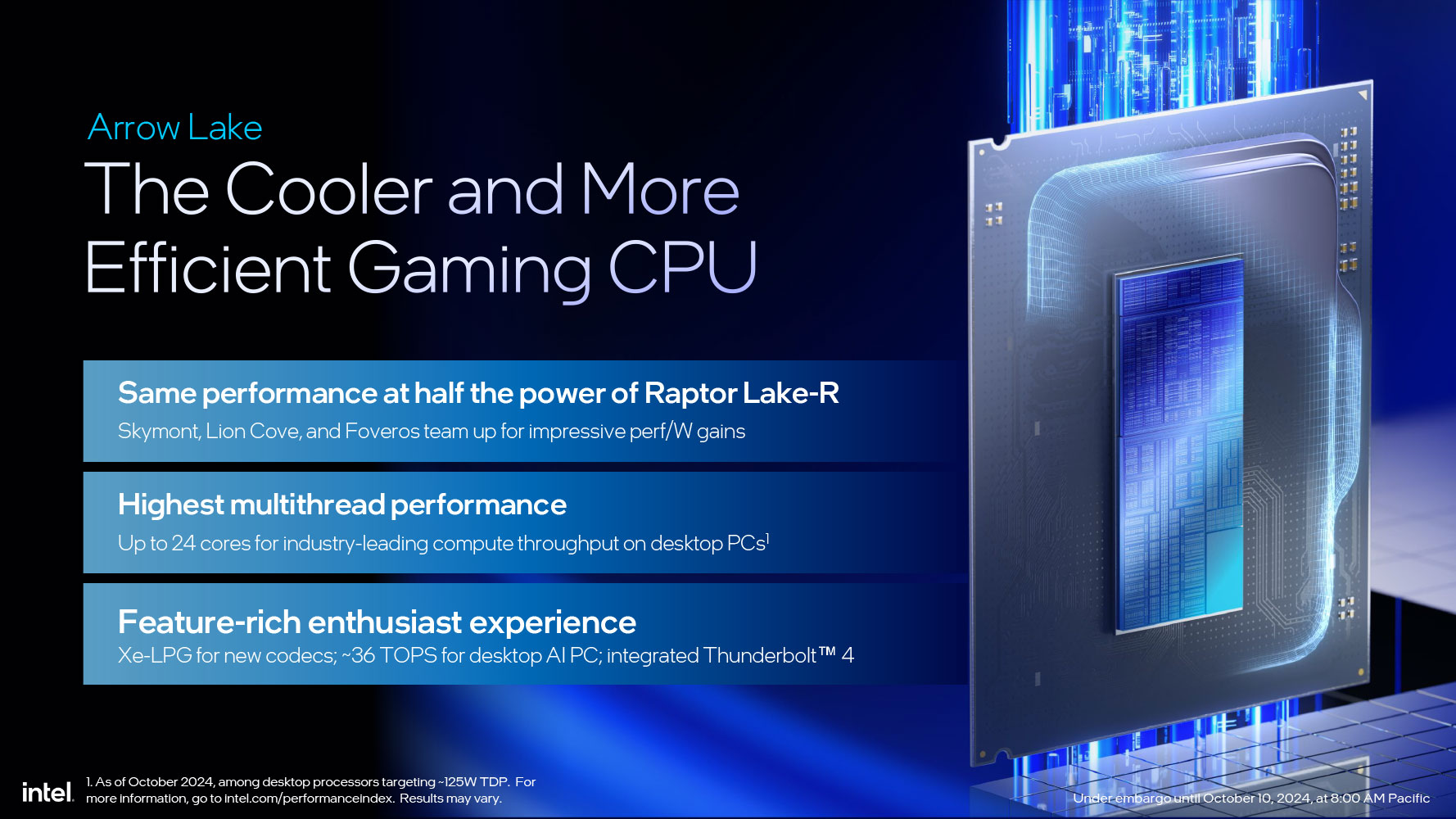
It's finally here! The hotly anticipated Core Ultra 9 285K Arrow Lake-S desktop processor is in our hands, and we can't wait to tell you all about it. The 285K is the flagship processor model from this generation, and logically succeeds the Core i9-14900K. It has all the cores this silicon has to offer—8P+16E, with all the on-chip technologies. It's also fully unlocked and ready for you to take it on an overclocking adventure. The Arrow Lake architecture denotes many firsts for Intel in the desktop market. Notably, this is the company's first desktop processor with a chiplet-based disaggregated design. The mobile segment got it with the Core Ultra Meteor Lake, and Intel has been making chiplet based Xeon Scalable server processors for a few years now. Intel is pricing the Core Ultra 9 285K at $589. Given its core-count and pricing, its apparent rivals from the AMD camp are the Ryzen 9 9950X Zen 5, and the Ryzen 9 7950X3D Zen 4.
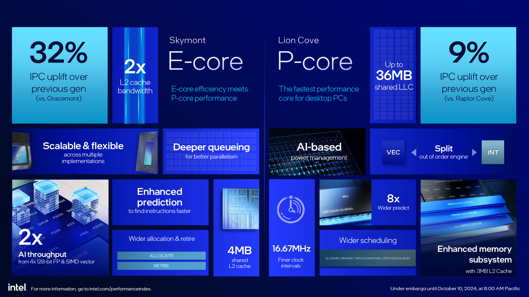
The Core Ultra 9 285K comes with a maxed out 8P+16E core-configuration. Intel has updated both core types with Arrow Lake. These amount to eight Lion Cove P-cores, with a nominal generational IPC increase, and 16 of the swanky new Skymont E-cores. Skymont was the star of the show with Lunar Lake, as Intel achieved a nearly 50% IPC leap over the Crestmont low-power island E-cores powering the previous generation Meteor Lake. With Arrow Lake, these Skymont cores achieve a 32% IPC jump over the Gracemont E-cores from Raptor Lake. Besides the increased IPC, these E-cores even run at higher clock speeds than Gracemont, which means multithreaded productivity workloads are in for a treat. The 285K is technically a 24-core/24-thread processor. The Lion Cove P-cores ditch SMT. So any gen-on-gen multithreaded performance improvements over the i9-14900K rest squarely on stronger cores and new technology, despite a decrease in total thread count.

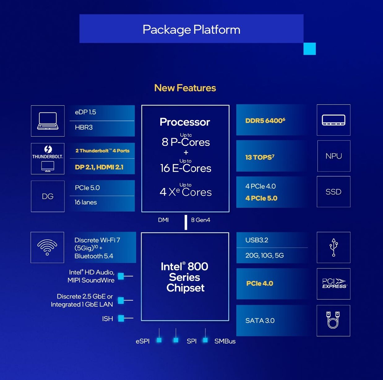
We've extensively detailed the Arrow Lake microarchitecture in our architecture preview article, which went live a couple of weeks ago. As we mentioned, this is Intel's first desktop processor that's based on chiplets. The guiding philosophy is that rather than building one large monolithic silicon on the latest foundry node (expensive, compounded by lower yields per wafer), Intel identifies specific IP blocks that benefit the most from a switch to the latest foundry node—in this case, the CPU complex—and build a chiplet with it that's smaller (higher yields per wafer thanks to smaller dies). The Compute tile houses the CPU cores, and is built on the TSMC N3B (3 nm) node, which is more advanced than the TSMC N4P (4 nm) node that AMD builds its Zen 5 CCDs on. With this, Intel is taking back foundry technology leadership from AMD after a long span of five years. The iGPU is built on a separate chiplet that uses the still fairly advanced 5 nm TSMC N5 node, while the rest of the processor with the various I/O controllers, and an integrated NPU, are built on TSMC 6 nm—same node as the cIOD on Ryzens.
This is Intel's first desktop processor with an NPU, but it isn't the latest NPU 4 from Intel that you find on Core Ultra 200V Lunar Lake mobile processors, but rather the older NPU 3 unit from Core Ultra 100 series Meteor Lake, which can only do 13 TOPS. It hence misses out on Microsoft Copilot+ native acceleration, but don't fret—there's still a lot you can do with 13 TOPS, Windows 11 can put the NPU to good use in its many in-built apps and utilities, and so can Microsoft Teams. Intel has given Arrow Lake-S a fairly powerful iGPU based on the Xe-LPG graphics architecture, and an updated media engine that can accelerate AV1 and HEVC encoding. There are a few changes to the I/O. For starters, DDR4 support is removed, as the memory controllers are re-engineered. The number of PCIe Gen 5 lanes from the CPU are increased to 20, so you can use a Gen 5 NVMe SSD without subtracting PCIe lanes from the x16 PEG slot. There's also integrated Thunderbolt 4.
Each of the eight Lion Cove P-cores on the 285K comes with a 3.70 GHz base frequency, and the P-cores boost up to 5.70 GHz. The classic Turbo Boost algorithm boosts P-cores up to 5.50 GHz. Turbo Boost Max 3.0 pushes a couple of cores up a notch to 5.60 GHz, and from there, provided your cooling solution is up to the task, Thermal Velocity Boost enables 5.70 GHz. The 16 E-cores, divided into four clusters, tick at 3.20 GHz with an impressive 4.60 GHz boost frequency. Each P-core comes with a dedicated 3 MB L2 cache, while each E-core cluster shares a 4 MB L2 cache among four E-cores. The P-cores and E-core clusters share a 36 MB L3 cache.
| Price | Cores / Threads | Base Clock | Max. Boost | L3 Cache | TDP | Architecture | Process | Socket | |
|---|---|---|---|---|---|---|---|---|---|
| Intel Core i5 | |||||||||
| Core i5-12400F | $110 | 6 / 12 | 2.5 GHz | 4.4 GHz | 18 MB | 65 W | Alder Lake | 10 nm | LGA 1700 |
| Core i5-13400F | $170 | 6+4 / 16 | 2.5 / 1.8 GHz | 4.6 / 3.3 GHz | 20 MB | 65 W | Raptor Lake | 10 nm | LGA 1700 |
| Core i5-12600K | $170 | 6+4 / 16 | 3.7 / 2.8 GHz | 4.9 / 3.6 GHz | 20 MB | 125 W | Alder Lake | 10 nm | LGA 1700 |
| Core i5-13600K | $225 | 6+8 / 20 | 3.5 / 2.6 GHz | 5.1 / 3.9 GHz | 24 MB | 125 W | Raptor Lake | 10 nm | LGA 1700 |
| Core i5-14600K | $260 | 6+8 / 20 | 3.5 / 2.6 GHz | 5.3 / 4.0 GHz | 24 MB | 125 W | Raptor Lake | 10 nm | LGA 1700 |
| Intel Core Ultra 5 | |||||||||
| Core Ultra 5 245K | $310 | 6+8 / 14 | 4.2 / 3.6 GHz | 5.2 / 4.6 GHz | 24 MB | 159 W | Arrow Lake | 3 nm | LGA 1851 |
| AMD Ryzen 5 | |||||||||
| Ryzen 5 8500G | $150 | 6 / 12 | 3.5 GHz | 5.0 GHz | 16 MB | 65 W | Phoenix 2 | 4 nm | AM5 |
| Ryzen 5 5600X | $135 | 6 / 12 | 3.7 GHz | 4.6 GHz | 32 MB | 65 W | Zen 3 | 7 nm | AM4 |
| Ryzen 5 7600 | $185 | 6 / 12 | 3.8 GHz | 5.1 GHz | 32 MB | 65 W | Zen 4 | 5 nm | AM5 |
| Ryzen 5 7600X | $210 | 6 / 12 | 4.7 GHz | 5.3 GHz | 32 MB | 105 W | Zen 4 | 5 nm | AM5 |
| Ryzen 5 9600X | $250 | 6 / 12 | 3.9 GHz | 5.4 GHz | 32 MB | 65 W | Zen 5 | 4 nm | AM5 |
| Intel Core i7 | |||||||||
| Core i7-12700K | $210 | 8+4 / 20 | 3.6 / 2.7 GHz | 5.0 / 3.8 GHz | 25 MB | 125 W | Alder Lake | 10 nm | LGA 1700 |
| Core i7-13700K | $280 | 8+8 / 24 | 3.4 / 2.5 GHz | 5.4 / 4.2 GHz | 30 MB | 125 W | Raptor Lake | 10 nm | LGA 1700 |
| Core i7-14700K | $355 | 8+12 / 28 | 3.4 / 2.5 GHz | 5.6 / 4.3 GHz | 33 MB | 125 W | Raptor Lake | 10 nm | LGA 1700 |
| Intel Core Ultra 7 | |||||||||
| Core Ultra 7 265K | $395 | 8+12 / 20 | 3.9 / 3.3 GHz | 5.5 / 4.6 GHz | 30 MB | 250 W | Arrow Lake | 3 nm | LGA 1851 |
| AMD Ryzen 7 | |||||||||
| Ryzen 7 5700G | $165 | 8 / 16 | 3.8 GHz | 4.6 GHz | 16 MB | 65 W | Zen 3 + Vega | 7 nm | AM4 |
| Ryzen 7 5700X | $160 | 8 / 16 | 3.4 GHz | 4.6 GHz | 32 MB | 65 W | Zen 3 | 7 nm | AM4 |
| Ryzen 7 7700 | $280 | 8 / 16 | 3.8 GHz | 5.3 GHz | 32 MB | 65 W | Zen 4 | 5 nm | AM5 |
| Ryzen 7 7700X | $275 | 8 / 16 | 4.5 GHz | 5.4 GHz | 32 MB | 105 W | Zen 4 | 5 nm | AM5 |
| Ryzen 7 9700X | $330 | 8 / 16 | 3.8 GHz | 5.5 GHz | 32 MB | 65 W | Zen 5 | 4 nm | AM5 |
| Ryzen 7 5800X | $165 | 8 / 16 | 3.8 GHz | 4.7 GHz | 32 MB | 105 W | Zen 3 | 7 nm | AM4 |
| Ryzen 7 5800X3D | $340 | 8 / 16 | 3.4 GHz | 4.5 GHz | 96 MB | 105 W | Zen 3 | 7 nm | AM4 |
| Ryzen 7 7800X3D | $470 | 8 / 16 | 4.2 GHz | 5.0 GHz | 96 MB | 120 W | Zen 4 | 5 nm | AM5 |
| Intel Core i9 | |||||||||
| Core i9-12900K | $280 | 8+8 / 24 | 3.2 / 2.4 GHz | 5.2 / 3.9 GHz | 30 MB | 125 W | Alder Lake | 10 nm | LGA 1700 |
| Core i9-13900K | $415 | 8+16 / 32 | 3.0 / 2.2 GHz | 5.8 / 4.3 GHz | 36 MB | 125 W | Raptor Lake | 10 nm | LGA 1700 |
| Core i9-14900K | $445 | 8+16 / 32 | 3.2 / 2.4 GHz | 6.0 / 4.4 GHz | 36 MB | 125 W | Raptor Lake | 10 nm | LGA 1700 |
| Intel Core Ultra 9 | |||||||||
| Core Ultra 9 285K | $590 | 8+16 / 24 | 3.7 / 3.2 GHz | 5.7 / 4.6 GHz | 36 MB | 250 W | Arrow Lake | 3 nm | LGA 1851 |
| AMD Ryzen 9 | |||||||||
| Ryzen 9 5900X | $265 | 12 / 24 | 3.7 GHz | 4.8 GHz | 64 MB | 105 W | Zen 3 | 7 nm | AM4 |
| Ryzen 9 7900 | $370 | 12 / 24 | 3.7 GHz | 5.4 GHz | 64 MB | 65 W | Zen 4 | 5 nm | AM5 |
| Ryzen 9 7900X | $400 | 12 / 24 | 4.7 GHz | 5.6 GHz | 64 MB | 170 W | Zen 4 | 5 nm | AM5 |
| Ryzen 9 7900X3D | $580 | 12 / 24 | 4.4 GHz | 5.6 GHz | 128 MB | 120 W | Zen 4 | 5 nm | AM5 |
| Ryzen 9 9900X | $430 | 12 / 24 | 4.4 GHz | 5.6 GHz | 64 MB | 120 W | Zen 5 | 4 nm | AM5 |
| Ryzen 9 5950X | $345 | 16 / 32 | 3.4 GHz | 4.9 GHz | 64 MB | 105 W | Zen 3 | 7 nm | AM4 |
| Ryzen 9 7950X | $510 | 16 / 32 | 4.5 GHz | 5.7 GHz | 64 MB | 170 W | Zen 4 | 5 nm | AM5 |
| Ryzen 9 7950X3D | $550 | 16 / 32 | 4.2 GHz | 5.7 GHz | 128 MB | 120 W | Zen 4 | 5 nm | AM5 |
| Ryzen 9 9950X | $600 | 16 / 32 | 4.3 GHz | 5.7 GHz | 64 MB | 170 W | Zen 5 | 4 nm | AM5 |
Arrow Lake Architecture
Intel Arrow Lake microarchitecture seeks to advance all key IP blocks of the processor—the CPU cores, the iGPU and platform I/O interfaces, as well as introduces an NPU; but with Intel's pivot to the latest TSMC 3 nm process (something even Apple's latest SoCs are on), there is a concerted effort to offer a leap in energy efficiency and thermals compared to Raptor Lake, which was built on 10 nm (how's that for a leap?). Of course, it's mighty expensive to build a large monolithic die on 3 nm, and so Intel implemented its second engineering pivot—to disaggregated tile-based processors arranged on an active interposer. Intel made this pivot on mobile with Meteor Lake and server with Sapphire Rapids, but it now arrives at the desktop.
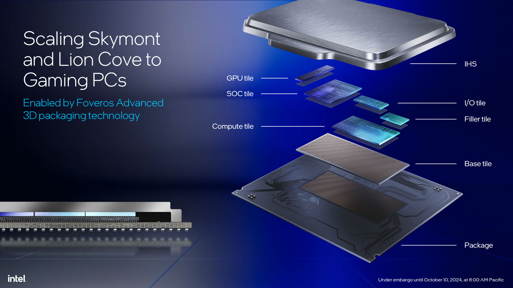
The CPU cores are located on a piece of silicon built on 3 nm, called the Compute tile. This talks to the SoC tile with the memory controllers and PCIe root, and can make do with TSMC 6 nm (the same node AMD uses for its I/O die). This SoC tile also includes Intel's NPU 3. The iGPU is located on a dedicated Graphics tile, which is built on a fairly advanced 5 nm process. All the tiles sit on a Foveros base-tile, which acts like an interposer, facilitating high-density microscopic connections among the tiles, and their connections to the fiberglass substrate below using through-silicon vias. Intel says that the die-area of Arrow Lake-S (8P+16E) is 243 mm², and its total transistor count is 17.8 billion.
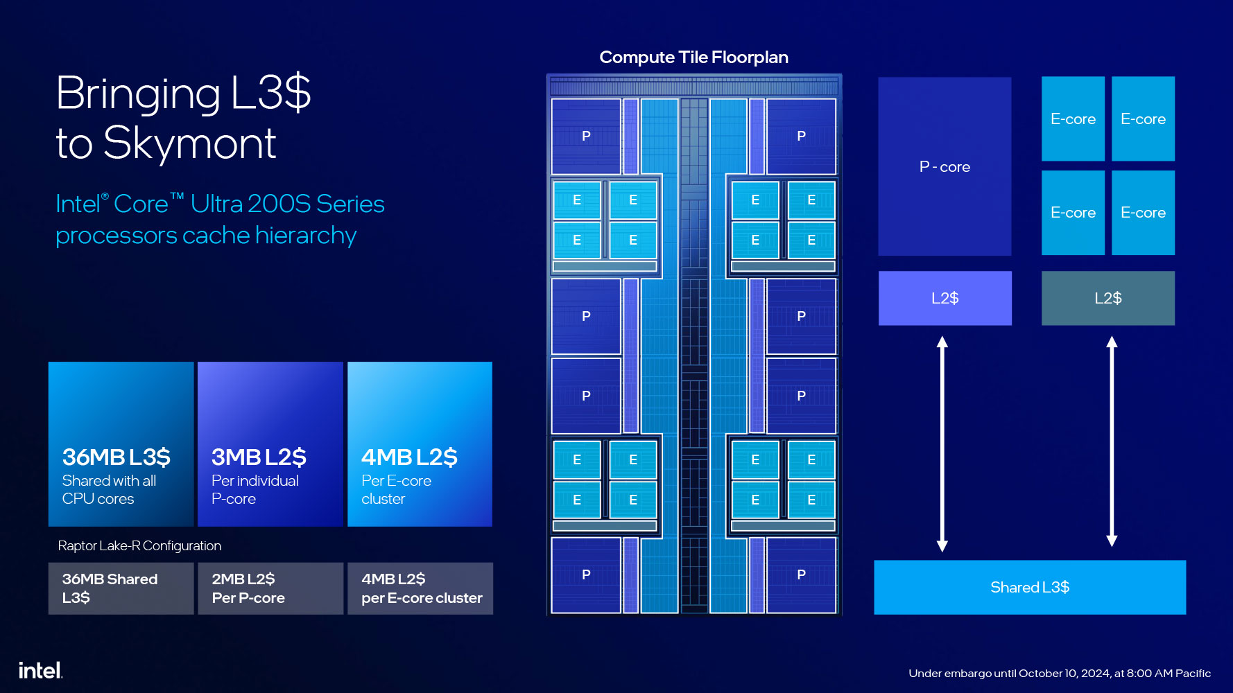
The Compute tile is the most important tile on the processor, it is dedicated to the CPU complex—the collective of 8 Lion Cove performance cores, and 16 Skymont E-cores. All 24 cores share a ringbus interconnect, and a 36 MB L3 cache. Each of the 8 P-cores has a 3 MB L3 cache, the E-cores are arranged in groups of 4 cores, called clusters. Each cluster shares a 4 MB L2 cache among its four cores. Unlike with Alder Lake and Raptor Lake, The P-cores and E-core clusters aren't segregated along two ends of the CPU, rather, they are arranged in alternating rows. There is a row of P-cores, followed by a row of two E-core clusters, and then two rows of P-cores, followed by another row of E-core clusters, and then the final row of P-cores. This approach has two benefits. Firstly, it reduces the concentration of heat during P-core intensive workloads such as gaming. Secondly, it could improve intercore latencies when threads are migrating between P-cores and E-cores, as it cuts down the ringbus stops between the two core types.
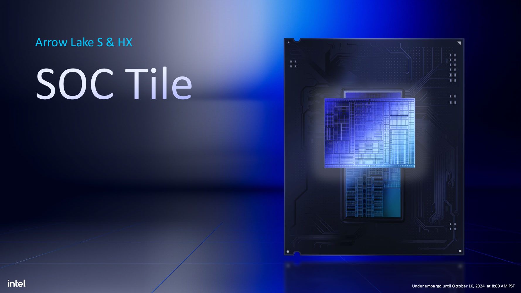
The SoC tile is the next most important tile. This takes up a mostly-central region of the chip, and is built on the 6 nm process. There are no low-power island E-cores on this tile, unlike with "Meteor Lake." The only logic heavy component is the NPU. This tile contains the dual-channel DDR5 memory controller, the DDR5 memory PHY, and the processor's PCI-Express root complex.
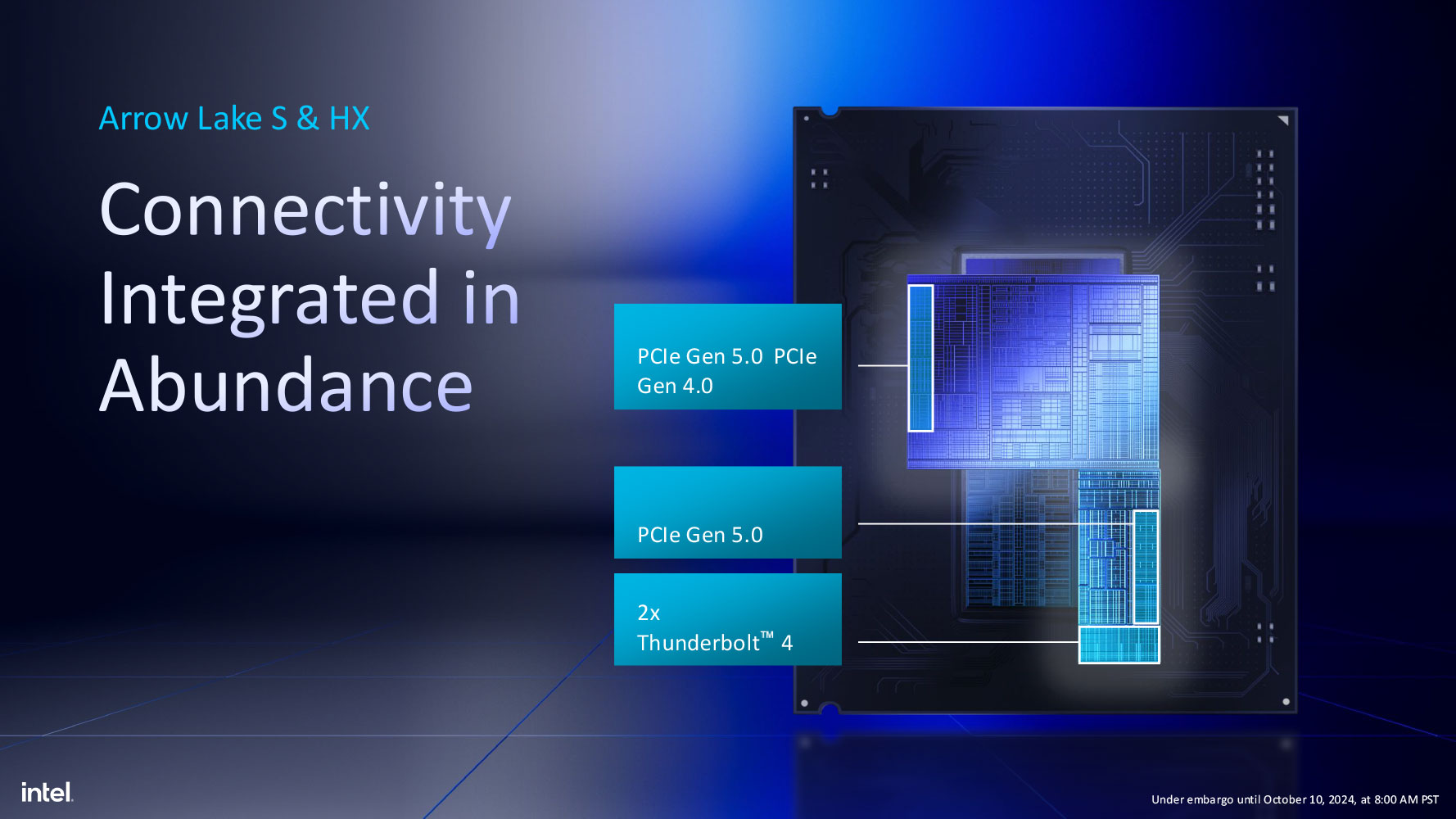
Not counting the DMI 4.0 x8 chipset bus, the processor puts out 20 PCIe Gen 5 lanes. Of these, 16 are dedicated to the PEG interface (for discrete graphics), and four to a dedicated CPU-attached M.2 NVMe slot. There are actually two CPU-attached M.2 slots. Besides the Gen 5 x4, there is a second Gen 4 x4 connection from the processor. This one comes from the breakout I/O tile, which also contains an integrated 40 Gbps Thunderbolt 4 controller. The SoC tile also contains three of the iGPU's allied components, the Display Engine, the Media Acceleration engine, and the Display I/O.
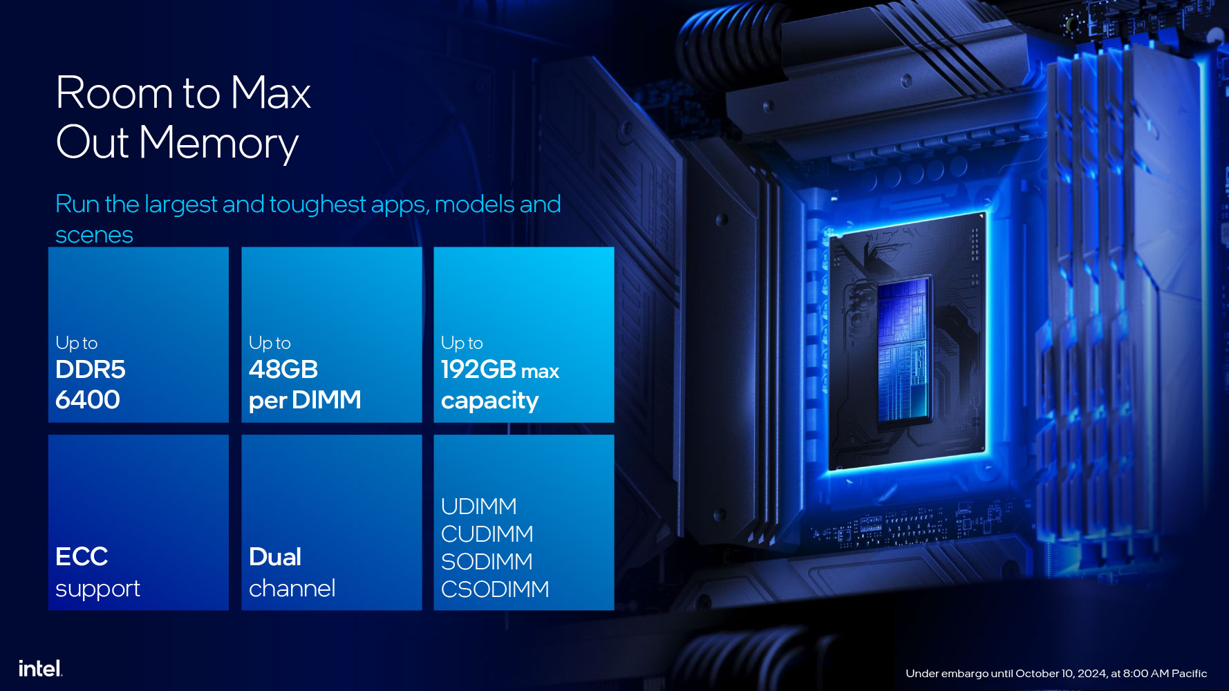

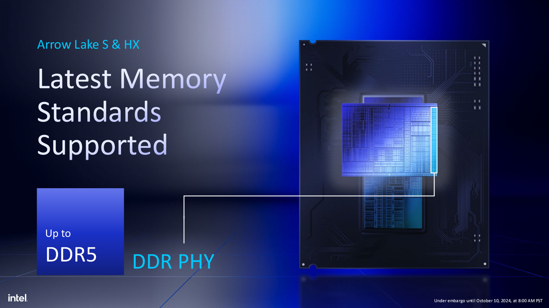
Intel deploys its second generation DDR5 memory controller architecture with Arrow Lake, retiring DDR4 memory support. The older Alder Lake and Raptor Lake feature a memory controller design with two controllers, each handling one channel, and both its 40-bit wide sub-channels; or in DDR4 mode, one controller per memory channel. Since Intel retired DDR4 support, the new architecture sees each of the two memory controllers address a sub-channel of a different channel. So controller 1 would address sub-channels 1 of both channels, while controller 2 would address sub-channels 2 of both channels. This approach probably lets Intel better utilize the sub-channel parallelism on DDR5.
Arrow Lake-S supports up to 192 GB of dual-channel memory, with up to 48 GB density per DIMM. It comes with native support for JEDEC DDR5-6400, and Intel says that DDR5-8000 is the "sweetspot" overclocking memory speed. The processors also support overclocked memory speeds well beyond this. There are already announcements of DDR5-9600, and throughout 2025 we should see memory speeds well beyond 10000 MT/s, using memory modules that use CKD chips (CUDIMMs or CSODIMMs). ECC is supported by the architecture, though not on the Z890 chipset, nor by the processor models being announced today.
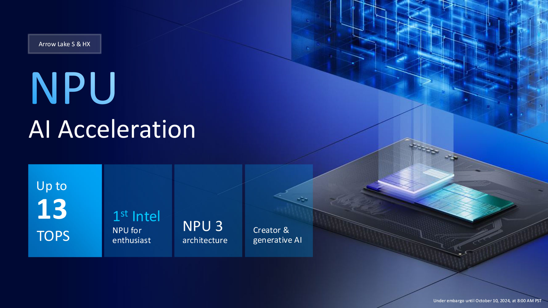
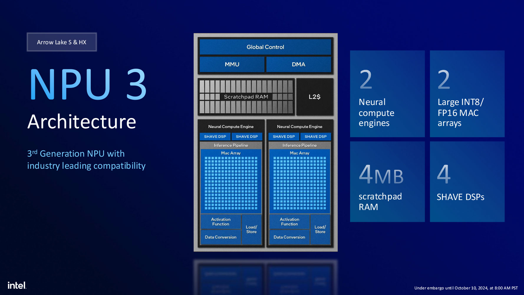
The SoC tile integrates an NPU 3 unit, which appears to have been carried over from "Meteor Lake." This is based on Intel's 3rd Gen NPU architecture, compared to the 4th Gen NPU on "Lunar Lake." NPU 3 has a peak throughput of 13 AI TOPS, which means it falls short of the 40 TOPS requirement for Microsoft Copilot+ local acceleration. The unit contains two NCEs (neural compute engines), with two INT8/FP16 MAC arrays, four SHAVE DSPs, and a 4 MB scratchpad RAM.
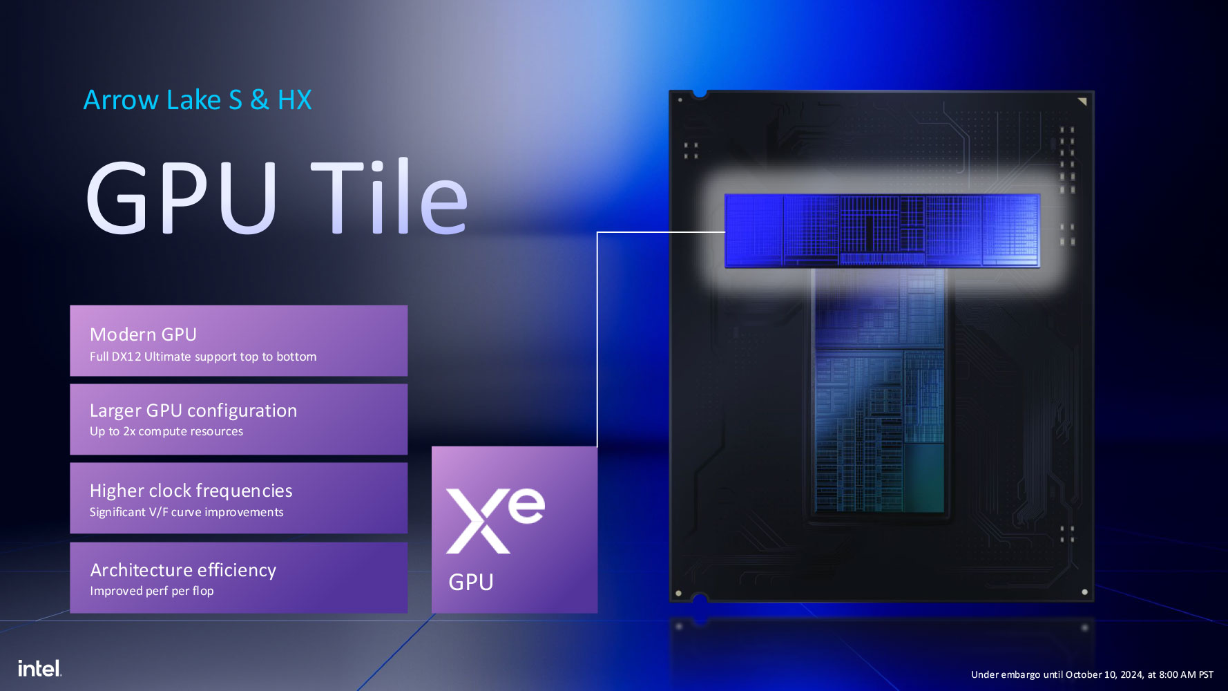
The third key tile of "Arrow Lake" is the Graphics tile, built on the Xe-LPG graphics architecture, which, interestingly, is a generation older than the Xe2 architecture powering the iGPU of "Lunar Lake." The Graphics tile is built on the 5 nm TSMC N5P node. This Graphics tile only contains the iGPU's number crunching and graphics rendering machinery, in the form of a single Xe Rendering Slice with four Xe cores, worth 64 execution units (EUs) or 512 unified shaders. The Xe cores of Arrow Lake's graphics tile lack XMX units. Any AI acceleration is in the form of DP4a, and not XMX. The enthusiast mobile "Arrow Lake-HX" uses the same Graphics tile. On the other hand, "Arrow Lake-H" comes with a larger Graphics tile with eight Xe cores (128 EU, 1,024 unified shaders), and the Xe cores there feature XMX units. Despite having just 4 Xe cores, the Graphics tiles of "Arrow Lake-S" and "Arrow Lake-HX" feature ray tracing units, one per Xe core, which give them full DirectX 12 Ultimate capability. Intel has also given the iGPU a rather large 4 MB L2 cache, which cushions transfers between it and the SoC tile.
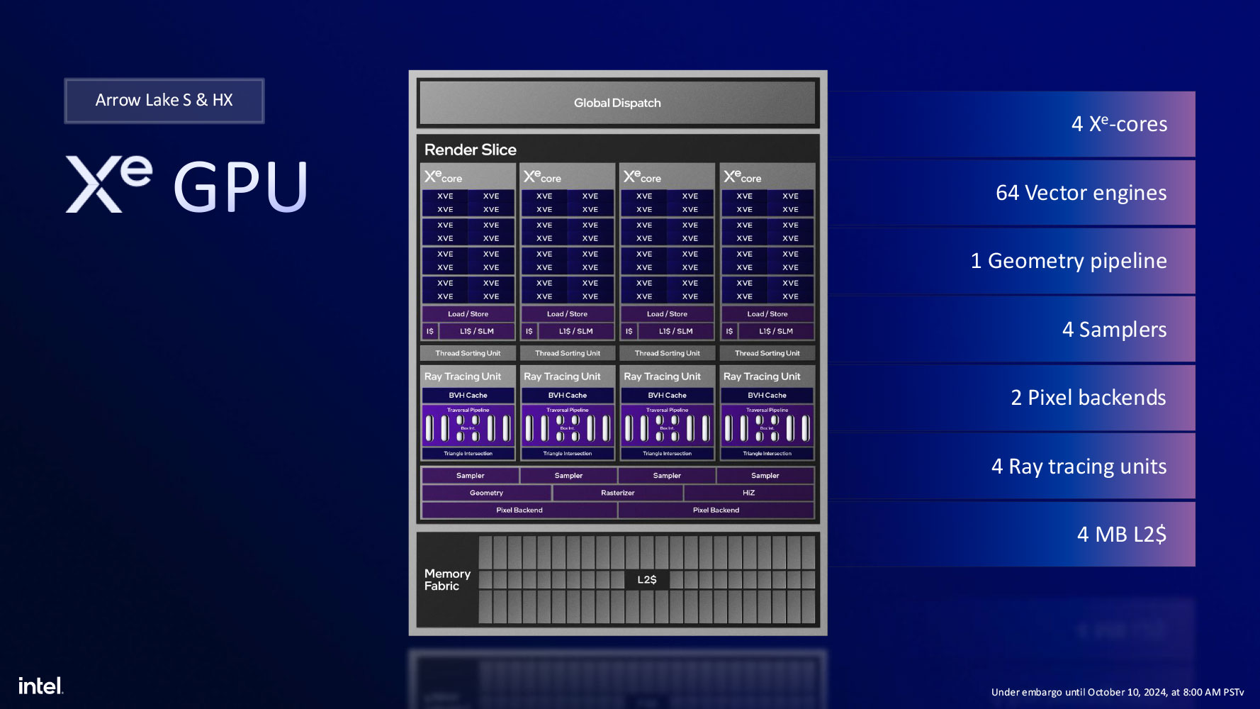
The Media Engine of "Arrow Lake-S" provides hardware-acceleration for video of up to 8K @ 60 Hz with 10-bit HDR, with supported formats that include VP9, AVC, HEVC, AV1, and SSC. Hardware-accelerated encoding is supported for resolutions of up to 8K @ 120 Hz with 10-bit HDR, with supported formats that include VP9, AVC, HEVC, and AV1. The Display Engine supports up to four display pipes with four low-power pipes, and support for up to five display ports. Standards supported include HDMI 2.1, DisplayPort 2.1, and eDP 1.4. Resolutions supported include 8K @ 60 Hz HDR, or four 4K @ 60 Hz HDR, or 1080p @ 360 Hz, or 1440p @ 360 Hz.
The Lion Cove P-core
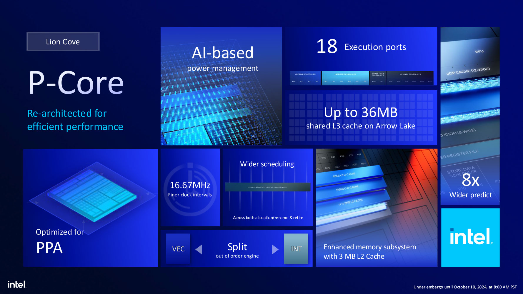
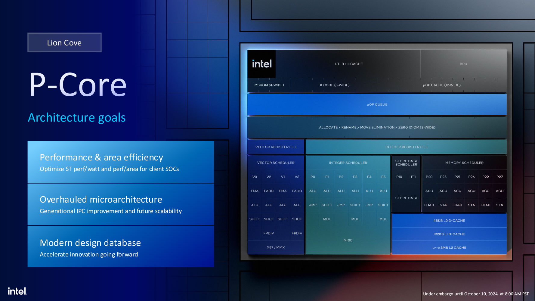
The new "Lion Cove" P-core replaces the "Raptor Cove" cores on the previous generation, as the main compute muscle of Arrow Lake. This is also the P-core on "Lunar Lake," and much like on that chip, the P-cores on Arrow Lake are arranged along a ring-bus with an L3 cache being shared among the P-cores. There is a slight cache difference, though, the dedicated L2 cache has been enlarged to 3 MB from 2.5 MB on the P-cores of Lunar Lake. The eight P-cores, along with the E-core clusters, share a 36 MB L3 cache, compared to the 12 MB on "Lunar Lake." Intel has come out with a new set of IPC gain claims for "Lion Cove." For "Arrow Lake," Intel claims a 9% IPC gain for "Lion Cove," compared to the "Raptor Cove" core of "Raptor Lake-S." In the "Lunar Lake" architecture reveal, the company claimed a 14% IPC gain, but that claim was made against the "Redwood Cove" P-core of a 15 W model of "Meteor Lake," since "Lunar Lake" is a one of a kind fully-integrated chip that has no predecessors except chips of a comparable power class from "Meteor Lake."
Much like on "Lunar Lake," the "Lion Cove" P-core of "Arrow Lake" lacks Hyper-Threading, Intel has physically removed the on-core components needed for SMT. This was done to reduce the size of the core, and with the idea that the IPC and energy-efficiency gains would overcome the need for SMT, together with physical threads on E-Cores. Having gained both die-area and power headroom from deprecating SMT, Intel moved on to overhauling the microarchitecture itself. There are improvements to all key components, including a redesigned front-end, with an 8 times larger branch prediction block. The fetch unit and decode bandwidth has been increased. The micro-op cache has increased in capacity, and Intel has introduced the concept of "nano-ops," which are groups of similar broken down micro-operation tasks that can be executed in tandem. The Integer and Vector domains, which form the out-of-order execution engine, has now split, with individual access to the micro-op queue, and independent schedulers. The out-of-order engine sees the allocation rename/move elimination queue to now be 8-wide compared to 6-wide on Redwood Cove. The retirement queue is broadened 50% to 12-wide from 8-wide. The instruction window depth has increased from 512 to 576. Execution ports have gone up from 12 to 18.
The Integer ALUs have increased in number from 5 to 6, with 3 jump units instead of 2, 3 shift units instead of 2, and three MUL units instead of 1. The vector execution engine sees 4 SIMD ALUs instead of 3, two FMA units @ 4 cycle, and 2 divider units. The load-store subsystem sees 128 DTLB size, up from 96, and 3 STE address generators instead of 2.
Intel has also redone the core-level cache subsystem, with the introduction of an intermediate data cache between the 48 KB L1 and L2. The L1D cache is now referred to as the L0 D-cache, which retires to a 192 KB L1 D-cache. This talks to the L2 cache. On Arrow Lake, each Lion Cove core gets 3 MB (3,072 KB) of dedicated L2 cache. Intel has deployed a new AI-based power management system for the P-cores, which is controlled by the SMU of the cores themselves. The CPU clock of the P-cores now have a fine 16.67 MHz granularity.
The Skymont E-core
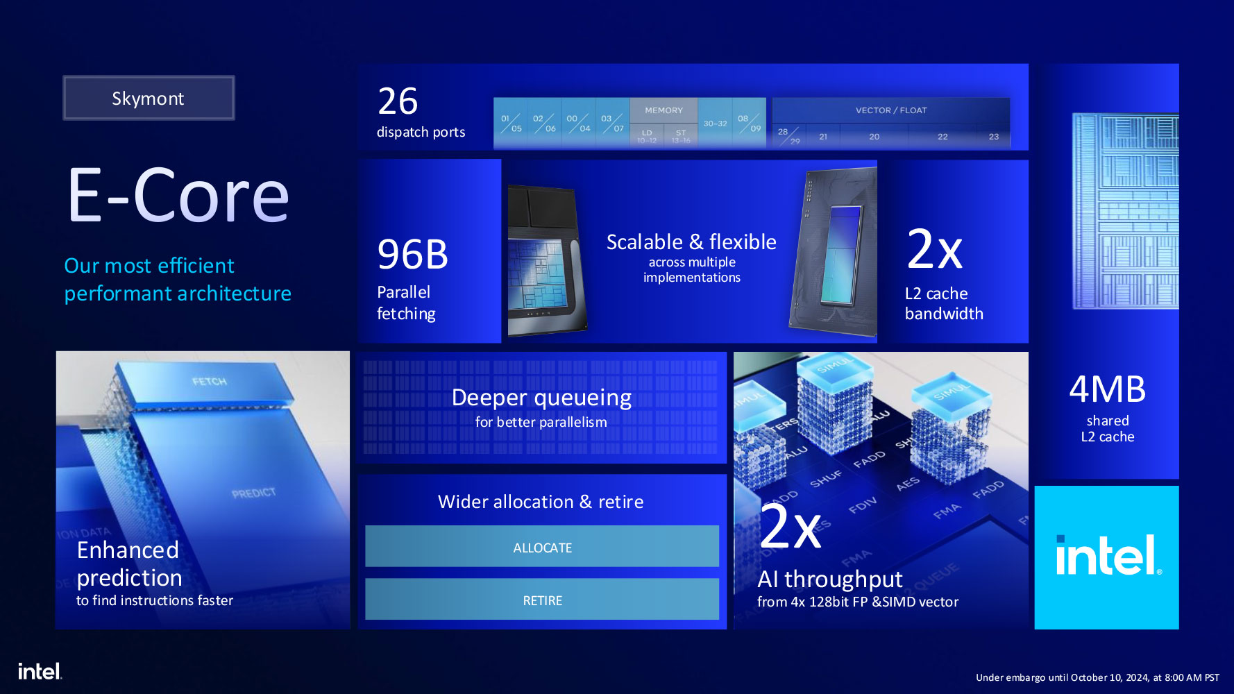
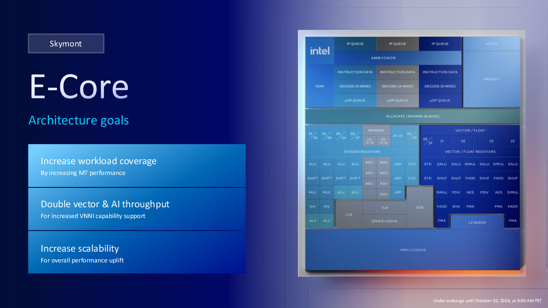
The new "Skymont" E-core was the single biggest talking point about "Lunar Lake." Intel achieved a 38% IPC uplift over the "Crestmont" E-cores of "Meteor Lake" in integer workloads, and a mammoth 68% IPC uplift over "Crestmont" in floating point workloads. There is a catch here. The E-cores on "Lunar Lake" are not part of a ring-bus with the P-cores (i.e. sharing their L3 cache), but separated out into a low-power island E-core cluster, and so Intel was making these IPC comparisons with the "Crestmont" low-power island E-cores of "Meteor Lake," located in the SoC tile. What's changed with "Arrow Lake" is that now all the "Skymont" E-core clusters are part of the Compute ring-bus, and share the L3 cache with the P-cores. The comparison is hence being made with the "Gracemont" E-cores of "Raptor Lake-S." All this said, the company claims a 32% IPC uplift over "Gracemont," which is still a mighty impressive generational gain.
This 32% IPC uplift of the "Skymont" E-cores on "Arrow Lake" play a crucial role in ensuring that the processor ends up posting generational gains in multithreaded productivity performance, despite the P-cores no longer featuring Hyper-Threading. The 16 E-cores on "Arrow Lake" are arranged in clusters of 4 cores each, and each cluster shares a 4 MB L2 cache among its cores. Intel claims to have doubled the bandwidth of this shared L2 cache compared to the "Gracemont" E-core clusters of "Raptor Lake-S."
Skymont's journey towards becoming something special begins with the fetch and branch prediction unit, which now looks 128 bytes ahead for possible branches, speeding up the instruction fetch. Up to 96 instruction bytes are fetched in parallel. The front-end sees a new 9-wide decode (compared to 6-wide on Crestmont), support for nano-code (similar segments of microcode clumped together for greater parallelism), and a broader micro-op queue of 96 entries instead of 64 on the previous generation.
The out-of-order engine sees the meat of the updates. The allocation queue is 8-wide (up from 6-wide), and the retire queue is 16-wide (up from 8-wide). There is intelligence behind dependency breaking. The out-of-order window is broadened to 416 entries, up from 256, as are the physical register files, reservation stations, and load-store unit buffering.
There are 26 dispatch ports to the execution engine, leading to 8 integer ALUs, with 3 jump ports, and 3 loads per cycle (50% increase).
The vector engine features four 128-bit FPUs, doubling GigaFLOPS. The FMUL, FADD, and FMA latencies are reduced. FP rounding now sees native hardware acceleration. Additional execution units should also benefit AI performance. The load/store unit sees 33% to 50% increases in loads, and store address generation performance. The L2 TLB has increased in size to 4,192 entries, up from 3,096.
Thread Director Updates
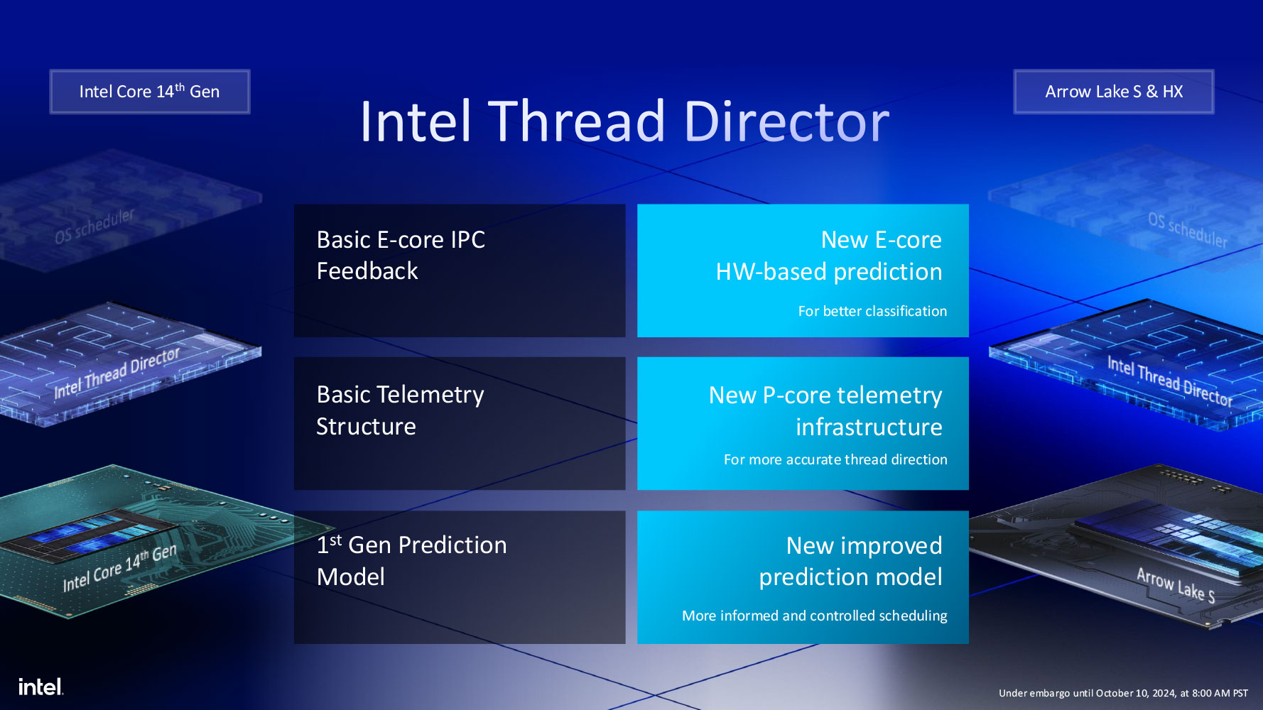
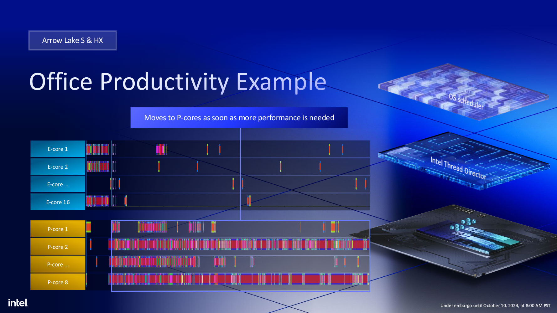
With "Arrow Lake," Intel is introducing the third generation of Thread Director, its hardware-based scheduler that ensures the right kind of software workload is handled by the right kind of CPU core. This new version comes with a more accurate hardware-based E-core performance feedback mechanism, which tells it the kind of E-core resources available. Intel also introduced new P-core performance telemetry for more accurate direction of threads to the P-cores. Intel also gave Thread Director its most accurate prediction model. With "Skymont" cores having such significantly higher IPC, Thread Director on "Arrow Lake-S" prioritizes all non-gaming productivity workloads to the E-cores, and upgrades threads to the P-cores only as needed. Thread Director plays a significant role in improving the processor's overall power efficiency.
Intel LGA1851 Platform
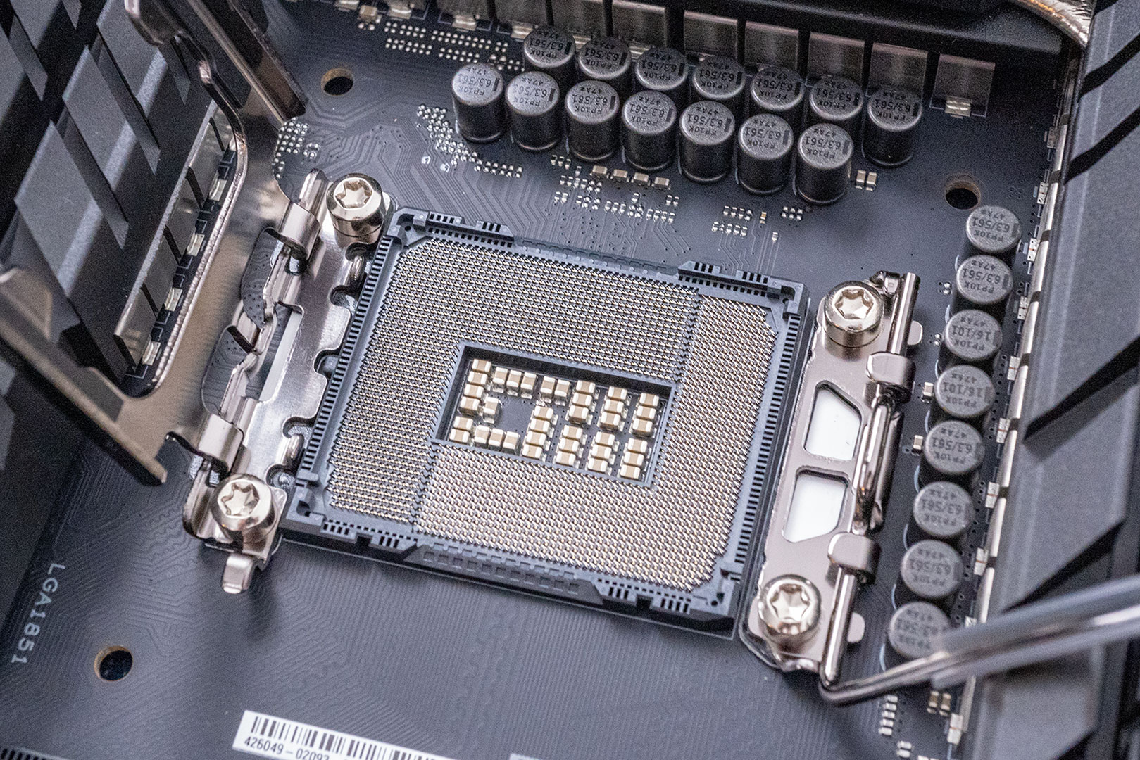
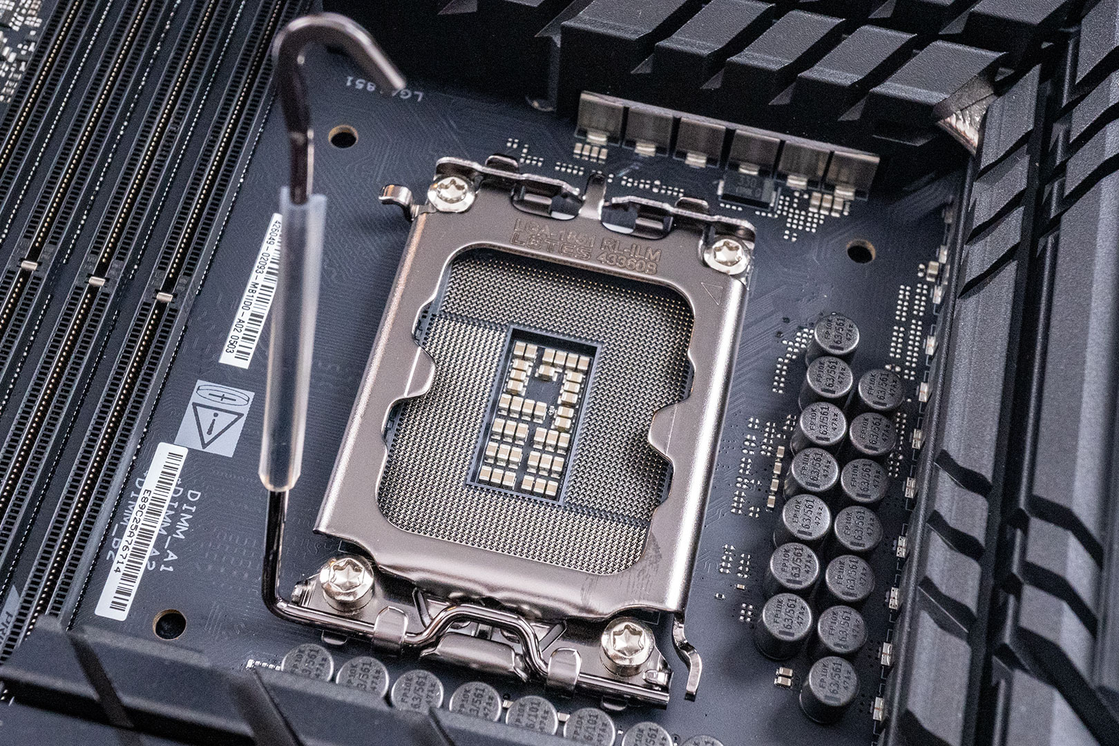
The new LGA1851 socket retains cooler compatibility with LGA1700. The processor packages have identical dimensions and Z-Height to help with this compatibility, too, but you cannot use an LGA1700 processor on an LGA1851 socket. Among other things, the additional pins are for the four extra PCIe Gen 5 lanes the processor puts out, for a CPU-attached Gen 5 NVMe SSD that doesn't eat into the PEG x16.
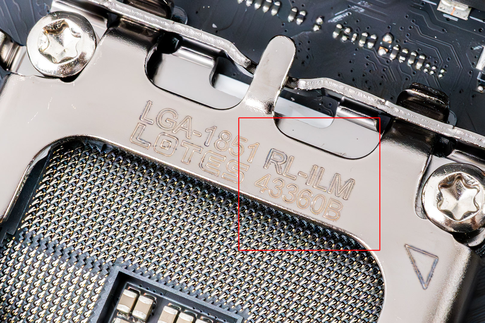
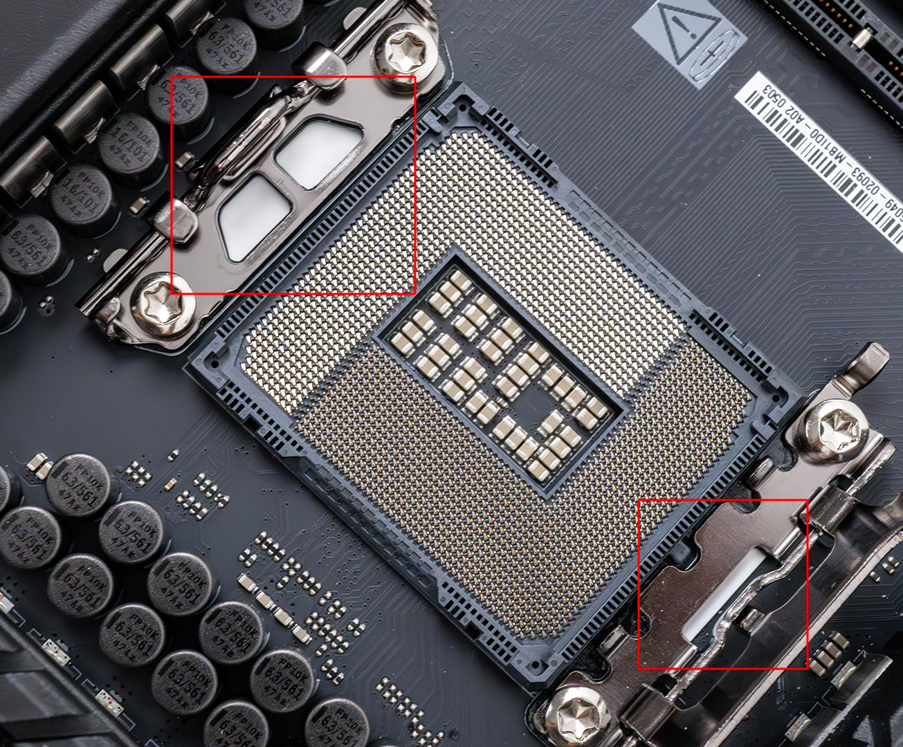
There are two kinds of ILM (independent loading modules) for the socket, some of the premium motherboard models include the new reduced load ILMs (RL-ILMs), which works to reduce mounting pressure on the package, letting you mount heavier coolers, such as LN2 evaporators. RL-ILMs are clearly marked on the metal brace. Another telltale is the presence of a white insulator pad under the ILM, near the mounting screws.
With the Core Ultra 2-series "Arrow Lake-S," Intel is debuting a new socket, LGA1851. You will hence require a new motherboard to go with your shiny new processor, and since all processor models Intel is launching this year are unlocked K or KF SKUs, the only motherboard chipset model available will be the top-spec Intel Z890. Intel will flesh out its processor model stack in 2025, and with it, launch more affordable motherboard chipsets.
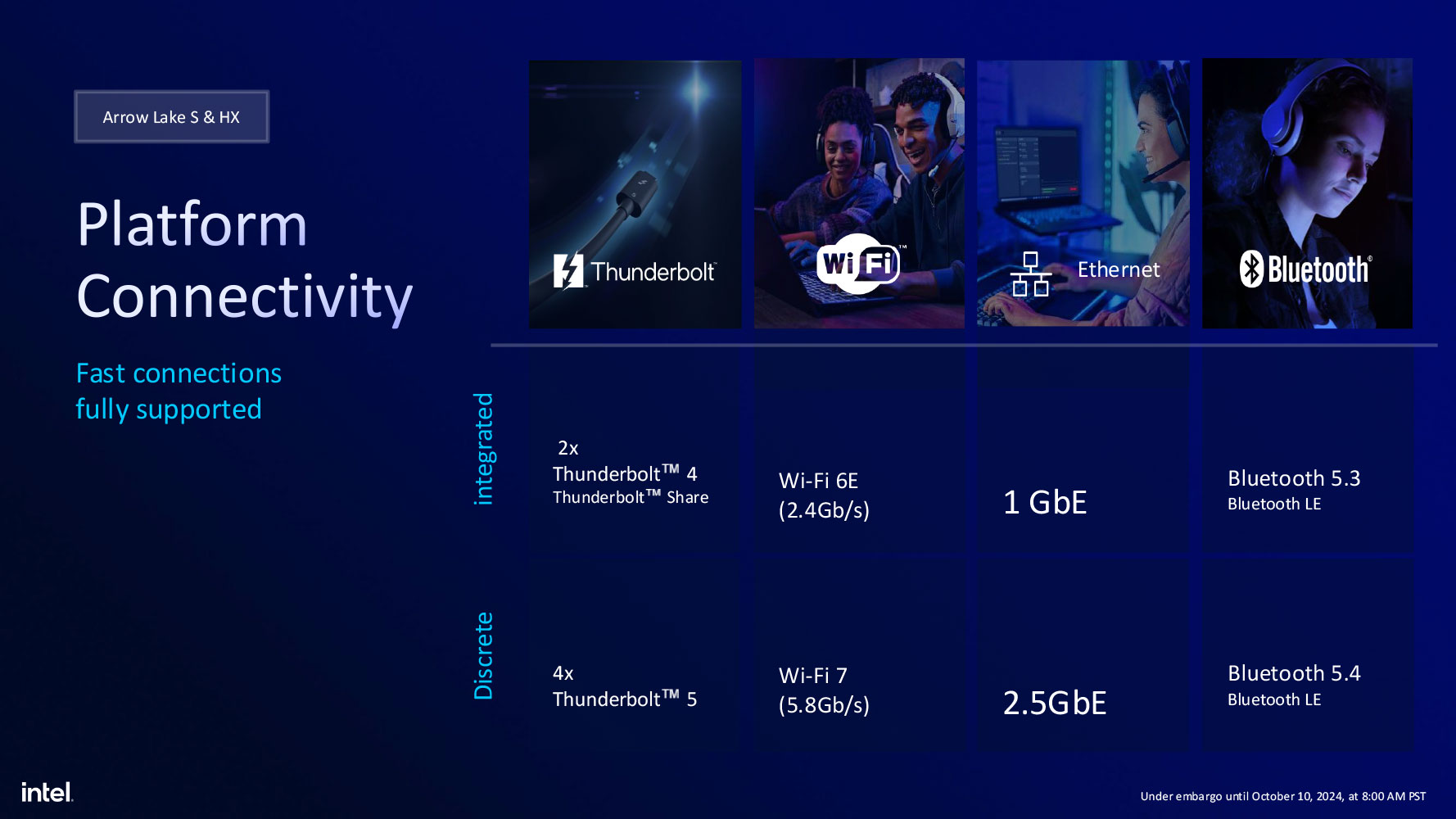
The "Arrow Lake-S" SoC puts out a dual-channel DDR5 memory interface, which we described in the previous pages. It also features a massive 48 platform PCIe lanes (CPU + chipset). Intel has increased the number of PCIe Gen 5 lanes put out by the CPU to 20—that's 16 lanes meant for the PEG (x16 slot for graphics cards), and one CPU-attached M.2 NVMe slot that runs at Gen 5 speeds without eating into the 16 PEG lanes. The CPU puts out a second set of Gen 4 x4, which can be wired out as an M.2 slot, or be used to drive high-bandwidth onboard devices, such as a discrete Thunderbolt 5 controller. The processor itself fully integrates a Thunderbolt 4 controller, which puts out a couple of 40 Gbps ports.
The processor connects to the Z890 chipset over a DMI 4.0 x8 chipset bus (bandwidth comparable to PCI-Express 4.0 x8). It puts out 24 PCI-Express Gen 4 downstream lanes. This is a massive increase from the Z790 chipset, which put out 16 Gen 4 and 8 Gen 3 lanes. The integrated USB complex consists of 32 USB 3.2 5 Gbps serial-deserializers, which can be configured by motherboard designers into five 20 Gbps ports, ten 10 Gbps ports, and ten 5 Gbps ports. There's also a 14-port USB 2.0 hub. Intel has retired the HDA "Azalia" audio interface with Z890, which means onboard audio CODECs will have to use the newer MIPI SoundWire and USB 3.2 interfaces (which CODECs like the Realtek ALC4080 and ALC4082 already do).

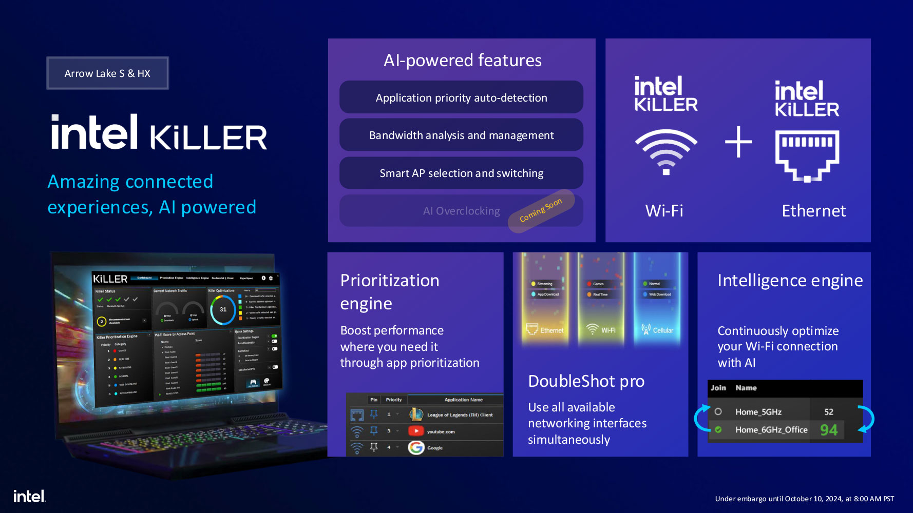
The chipset integrates a 1 GbE MAC, and Wi-Fi 6. With the PCIe and USB 3.2 connectivity on offer, motherboard vendors can go bonkers with network connectivity, by giving their platforms Wi-Fi 7 and 2.5 GbE, or even 5 GbE and 10 GbE. Vendors can opt for Intel's Killer networking package, which combines existing Intel networking PHY with the advanced Killer prioritization engine, and DoubleShot Pro, which work together to reduce network latency when gaming. Intel has revamped the security architecture for its client processors with "Arrow Lake," giving them three separate hardware security engines, including a purpose-built Converged Security and Manageability Engine (basically the Intel ME but with added security roles), the Silicon Security Engine, which is microarchitecture-level hardening for the new Lion Cove and Skymont CPU cores, a new dedicated security controller for the iGPU, and compliance with Microsoft Secured Core.
Overclocking
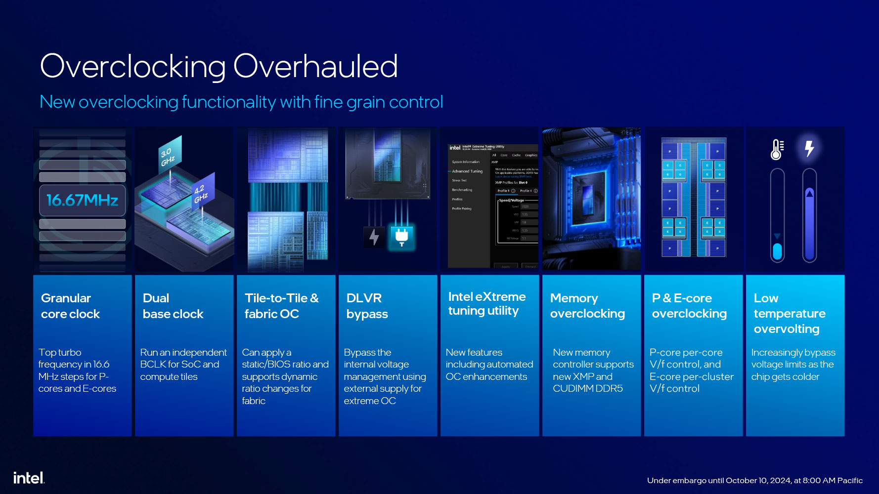
The governing idea behind Arrow Lake is to offer generational performance gains along expected lines, but with a leap in energy efficiency from the new tile-based disaggregation, and switch to the new 3 nm foundry node for key logic components of the chip. Conversely, this means that the high efficiency opens up some overclocking headroom. Arrow Lake introduces a dual base-clock domain architecture. There are now two independent BCLK domains, one for the Compute tile, and the other for the SoC tile. This is crucial in ensuring that BCLK-based overclocking doesn't destabilize other clock domains such as PCIe clock, which will stick to the BCLK domain of the SoC tile.
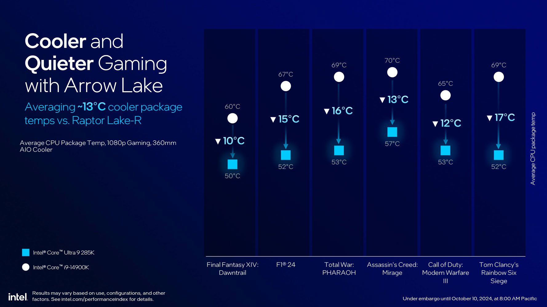
Next up, Intel added a granularity of 16.67 MHz for the clock speeds of the P-cores and E-cores, letting you fine-tune your overclock that much better. The tile-to-tile fabric has a clock domain of its own, which can either be overclocked with a static frequency setting, or in a ratio with CPU clock speeds. DLVR (digital linear voltage regulator) bypass lets certain premium motherboards override the internal voltage management of the processor with smart discrete voltage regulation controllers for superior OC. Arrow Lake supports V/f curve control on a per P-core and per E-core cluster basis. The processor's SMU can detect low-temperature cooling solutions in an overclocked scenario, and bypass voltage limits as the chip gets cooler. Lastly, "Arrow Lake" offers native support for CUDIMMs and CSODIMMs. These are DDR5 memory modules with CKD (client clock drivers), which clean up signal integrity, improving the memory signal eyes and allowing for higher frequencies. Some of the newer memory kits with over 8000 MT/s XMP tend to be CUDIMMs. The revamped power management, switch to the newer TSMC 3 nm node (where it matters), and other optimizations mean that besides lower power, the average package temperature of the 285K is around 13°C lower than that of the i9-14900K. In lightly threaded use-cases, Intel claims an up to 58% lower package power than the i9-14900K.
Unboxing and Photography
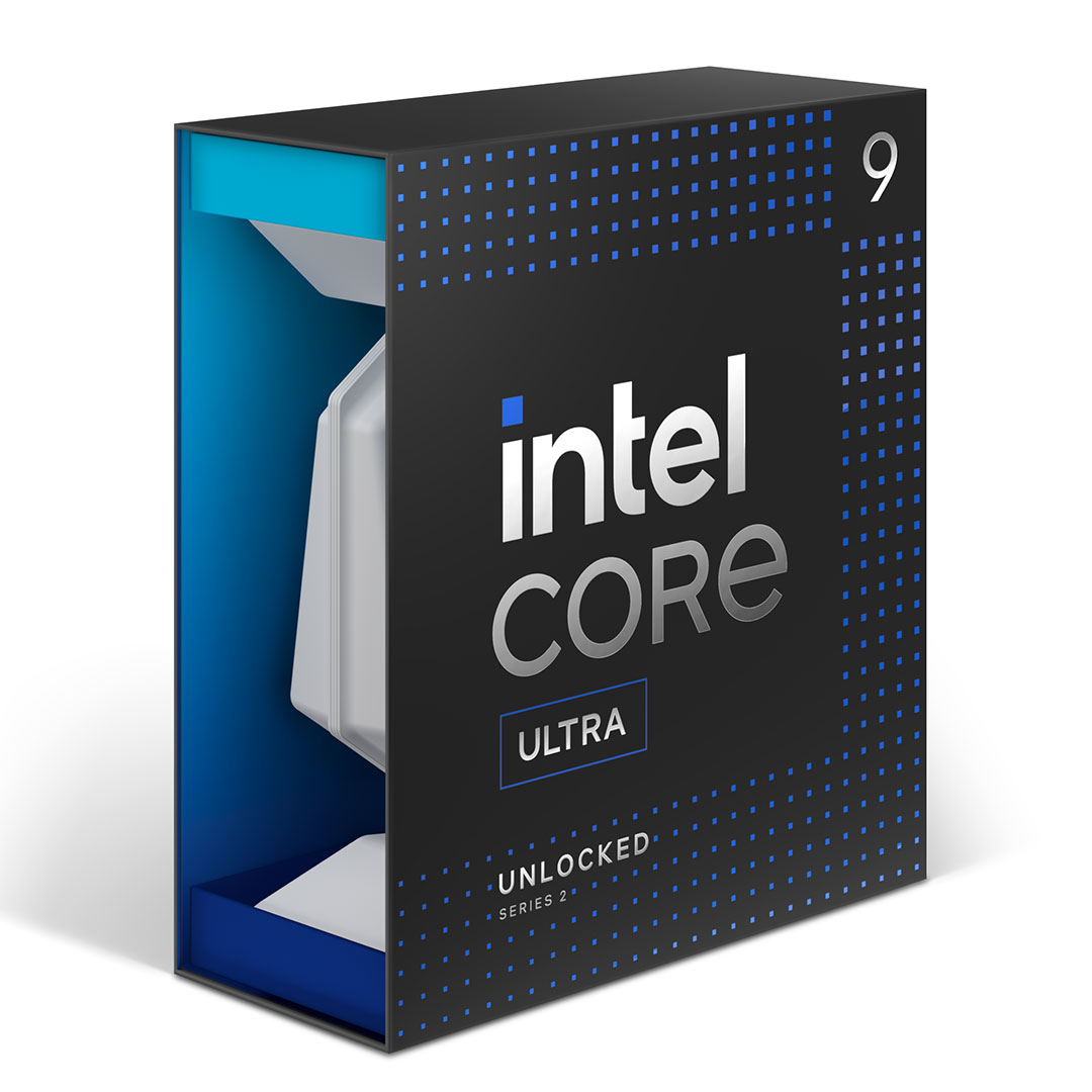
The Intel Core Ultra 9 285K comes in a special retail packaging. The processor is enclosed in a jewel-case that peeks out of the side. The front face of the box has some reflective bits that set it apart from retail boxes of other processor models in the series.
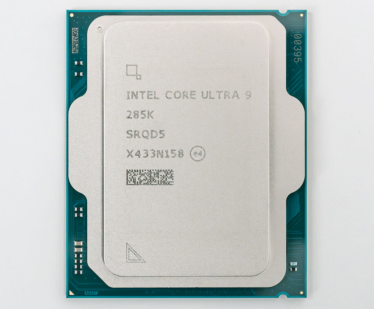
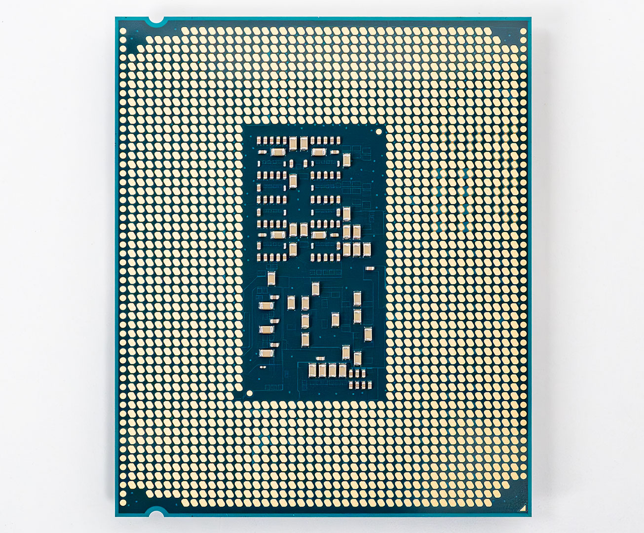
This looks like an LGA1700 CPU, but trust us, it won't fit on your older motherboard. The dimensions are identical to ensure cooler compatibility, but the key notch is different. Intel created space for those 151 extra pins by reducing the "island" in the middle of the land-grid.
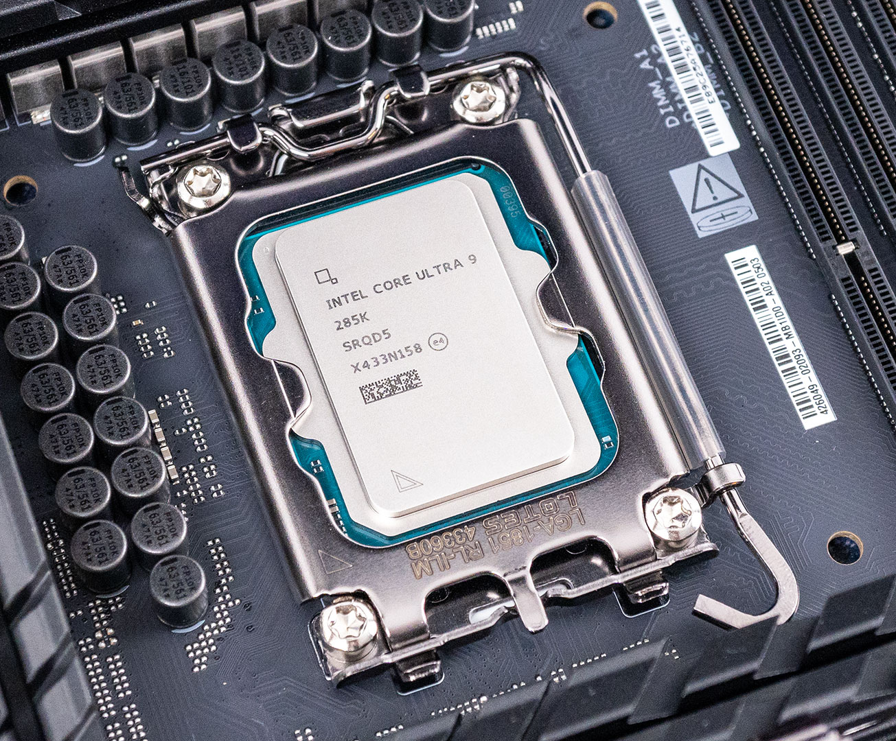
Installing an LGA1851 processor is identical to that of an LGA1700 processor.
Test Setup
- All applications, games, and processors are tested with the drivers and hardware listed below—no performance results were recycled between test systems.
- All games and applications are tested using the same version.
- All games are set to their highest quality setting unless indicated otherwise.
- Now that DDR5 has gained some maturity, we will use faster DDR5 speeds with tighter timings in upcoming reviews (once we retest the 40+ CPUs in our test group)
- The ASUS Z890 Hero motherboard feeds four of the CPU VRM phases from the 24-pin ATX connector, instead of the 8-pins, which makes it impossible to measure CPU-only power with dedicated test equipment (we're not trusting any CPU software power sensors). You either lose some power because only the two 8-pin CPU connectors are measured, or you end up including power for the GPU, chips, and storage when measuring the two 8-pin connectors along with the 24-pin ATX. For this reason, we used an MSI Z890 Carbon for the power consumption tests in this review.
| Test System "Arrow Lake" | |
|---|---|
| Processor: | All Intel Core 200 Series processors (Intel stock power settings / ASUS MCE disabled) |
| Motherboard: | ASUS Z890 Maximus Hero BIOS 0805 MSI Z890 Carbon (power consumption tests) BIOS 1A2T |
| Memory: | 2x 16 GB DDR5-6000 36-36-36-76 2T / Gear 2 |
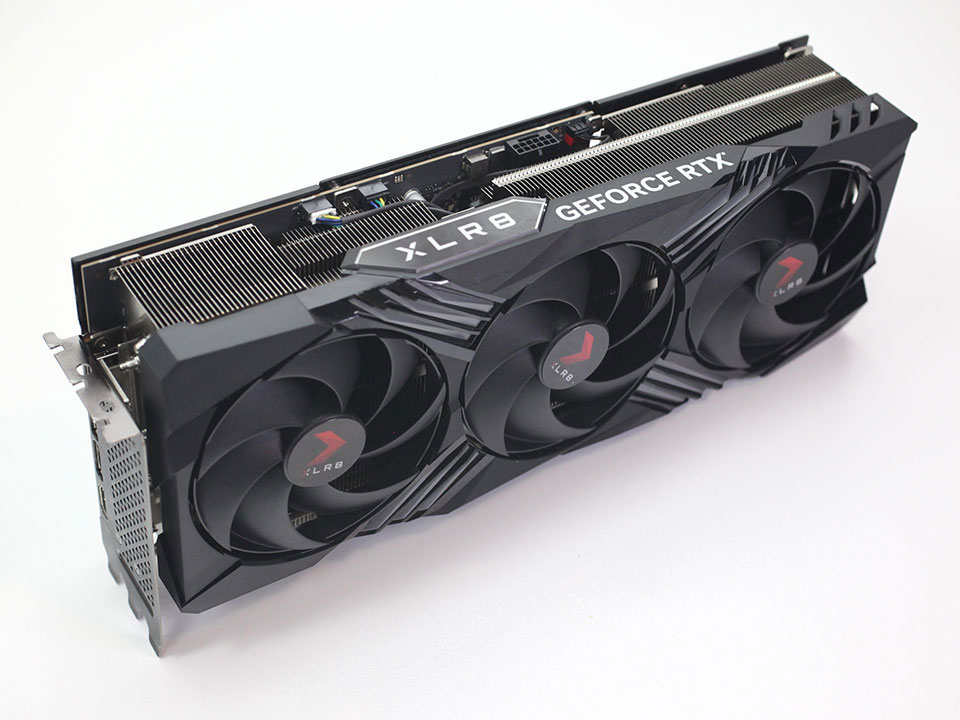
| Graphics: | PNY GeForce RTX 4090 XLR8 |
| Storage: | 2 TB M.2 NVMe SSD |
| Air Cooling: | Noctua NH-D15 |
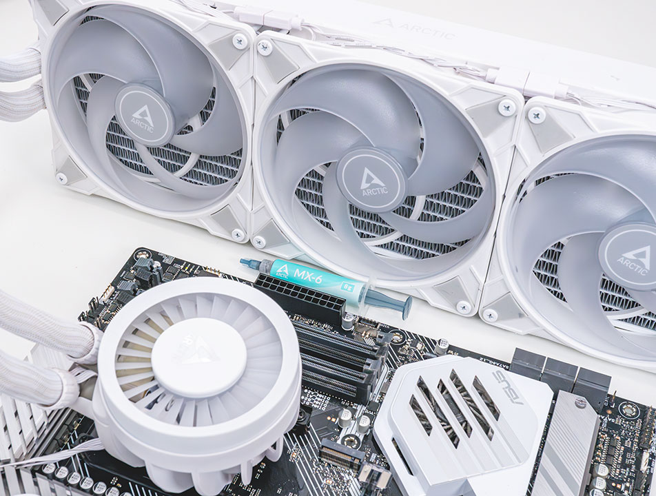
| Water Cooling: | Arctic Liquid Freezer III 420 mm AIO |
| Thermal Paste: | Arctic MX-6 |
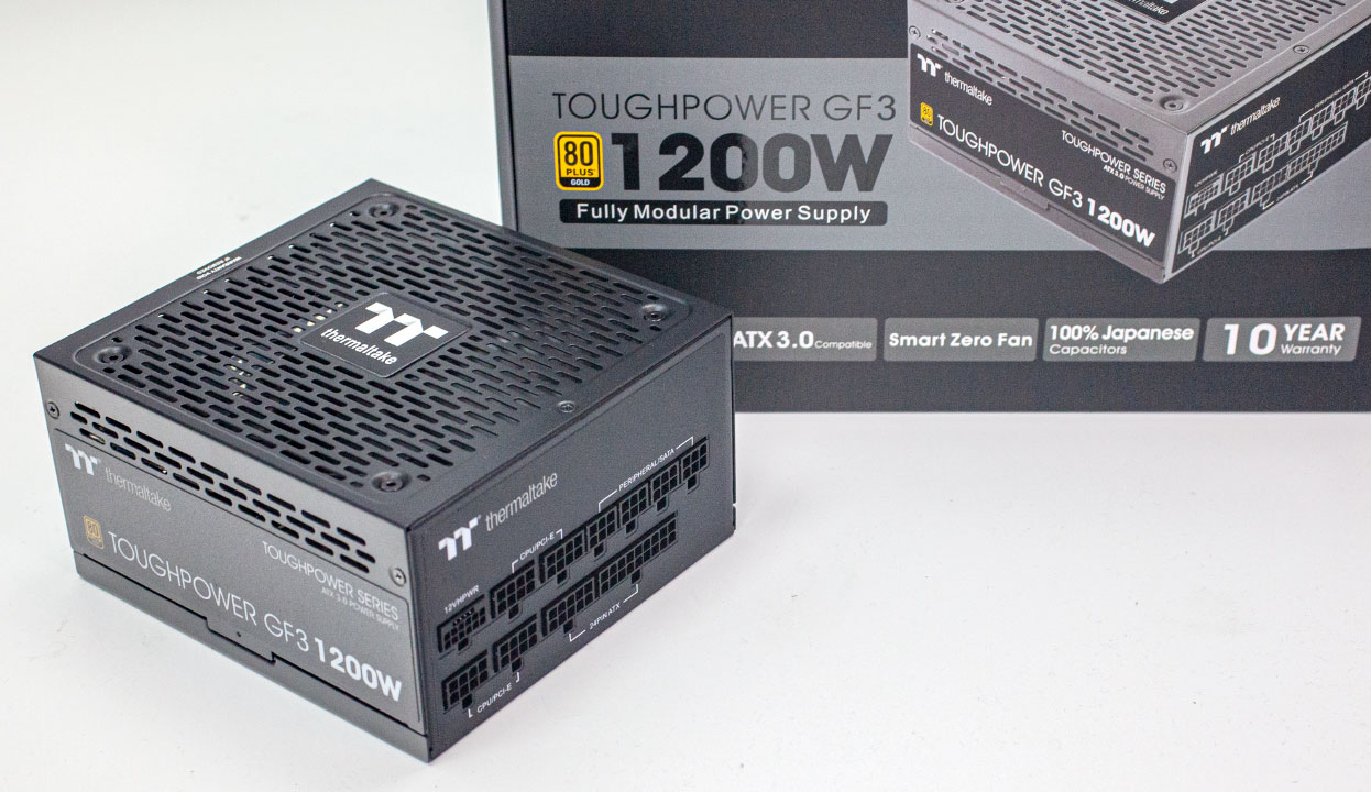
| Power Supply: | Thermaltake Toughpower GF3 1200 W ATX 3.0 / 16-pin 12VHPWR |
| Software: | Windows 11 Professional 64-bit 23H2 VBS enabled (Windows 11 default) |
| Drivers: | NVIDIA GeForce 555.85 WHQL |
| Test System "Zen 4 & Zen 5" | |
|---|---|
| Processor: | All AMD Ryzen 9000, 8000 & Ryzen 7000 processors |
| Motherboard: | ASUS X670E Crosshair Hero BIOS 2007 Ryzen 9000: BIOS 2201 |
| Memory: | 2x 16 GB DDR5-6000 36-36-36-76 Infinity Fabric @ 2000 MHz |
| Drivers: | Ryzen Chipset Drivers 6.05.28.016 Ryzen 9000: 6.06.28.910 Ryzen 9900X & 9950X: Game Mode enabled, Game Bar installed and active |
| All other specifications same as above | |
| Test System "Raptor Lake & Alder Lake" | |
|---|---|
| Processor: | All Intel 14th, 13th & 12th Gen processors (Intel stock power settings / ASUS MCE disabled) |
| Motherboard: | ASUS Z790 Maximus Dark Hero BIOS 1302 |
| Memory: | 2x 16 GB DDR5-6000 36-36-36-76 2T / Gear 2 |
| All other specifications same as above | |
| Test System "Zen 3 & Zen 2" | |
|---|---|
| Processor: | All AMD Ryzen 5000 & Ryzen 3000 processors |
| Motherboard: | ASUS X570 Crosshair VII Dark Hero BIOS 4805 |
| Memory: | 2x 16 GB DDR4-3600 14-14-14-34 1T Infinity Fabric @ 1800 MHz 1:1 |
| Drivers: | Ryzen Chipset Drivers 6.05.28.016 |
| All other specifications same as above | |
| Test System "Rocket Lake" | |
|---|---|
| Processor: | All Intel 11th Gen processors (Intel stock power settings / ASUS MCE disabled) |
| Motherboard: | ASUS Z590 Maximus XIII Hero BIOS 1701 |
| Memory: | 2x 16 GB DDR4-3600 14-14-14-34 1T Gear 1 |
| All other specifications same as above | |
| Test System "Zen 1" | |
|---|---|
| Processor: | All AMD Ryzen 2000 processors |
| Motherboard: | ASUS X570 Crosshair VII Dark Hero BIOS 4805 |
| Memory: | 2x 16 GB DDR4-3400 14-14-14-34 1T |
| All other specifications same as above | |
AIDA64 Cache and Memory Performance
In this first test we're looking at the performance offered by the memory subsystem and the processor's L1, L2 and L3 caches. AIDA64 comes with a great benchmark that provides a nice overview of all these performance characteristics.
Our Patreon Silver Supporters can read articles in single-page format.
May 6th, 2025 15:57 EDT
change timezone
Latest GPU Drivers
New Forum Posts
- need help choosing a CPU (3)
- What is the latest game you finished or 100% (22)
- RX 9000 series GPU Owners Club (673)
- Not thermal throttling, not power throttling, and yet still... throttling - lenovo laptop, i5 9300H (1)
- Game Soundtracks You Love (1062)
- How high of a ram frequency can i run on a Z690 with an 14700Kf processor? (7)
- Gigabyte graphic card - TIM GEL application failure? (25)
- What are you playing? (23556)
- Request for advice [Big Build] (65)
- 7900XT - Lower my GPU too constatly be running 500-600rpm (42)
Popular Reviews
- Arctic Liquid Freezer III Pro 360 A-RGB Review
- ASUS Radeon RX 9070 XT TUF OC Review
- Clair Obscur: Expedition 33 Performance Benchmark Review - 33 GPUs Tested
- ASUS ROG Maximus Z890 Hero Review
- Zotac GeForce RTX 5070 Ti Amp Extreme Review
- Upcoming Hardware Launches 2025 (Updated Apr 2025)
- Seasonic Vertex GX 850 W Review
- Sapphire Radeon RX 9070 XT Nitro+ Review - Beating NVIDIA
- ASUS GeForce RTX 5090 Astral Liquid OC Review - The Most Expensive GPU I've Ever Tested
- AMD Ryzen 7 9800X3D Review - The Best Gaming Processor
Controversial News Posts
- AMD Radeon RX 9060 XT to Roll Out 8 GB GDDR6 Edition, Despite Rumors (142)
- NVIDIA Sends MSRP Numbers to Partners: GeForce RTX 5060 Ti 8 GB at $379, RTX 5060 Ti 16 GB at $429 (128)
- NVIDIA Launches GeForce RTX 5060 Series, Beginning with RTX 5060 Ti This Week (115)
- Nintendo Confirms That Switch 2 Joy-Cons Will Not Utilize Hall Effect Stick Technology (105)
- Sony Increases the PS5 Pricing in EMEA and ANZ by Around 25 Percent (84)
- Parts of NVIDIA GeForce RTX 50 Series GPU PCB Reach Over 100°C: Report (78)
- Intel "Bartlett Lake-S" Gaming CPU is Possible, More Hints Appear for a 12 P-Core SKU (77)
- China Develops HDMI Alternative: 192 Gbps Speeds and 480 W Power Delivery (74)