 73
73
MSI GeForce GTX 1650 Gaming X 4 GB Review
Test Setup »High-resolution PCB Pictures
These pictures are for the convenience of volt-modders and those who would like to see all the finer details on the PCB. Feel free to link back to us and use them in your articles or forum posts.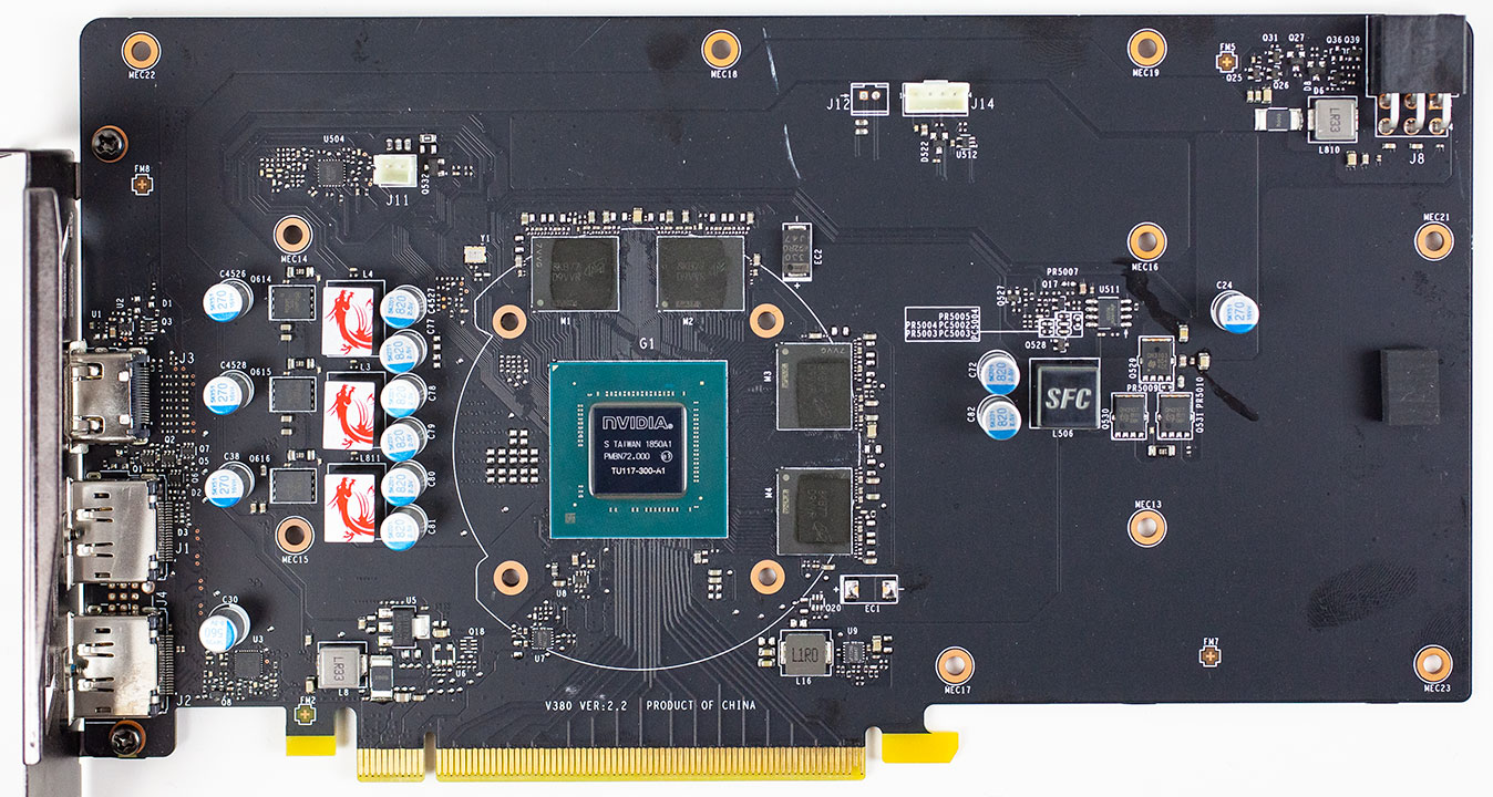

High-res versions are also available (front, back).
Circuit Board (PCB) Analysis
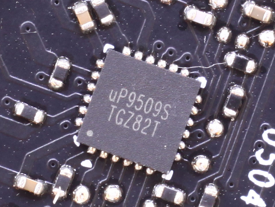
The GPU VRM is 3-phase, controlled by a uPI uP9509S.
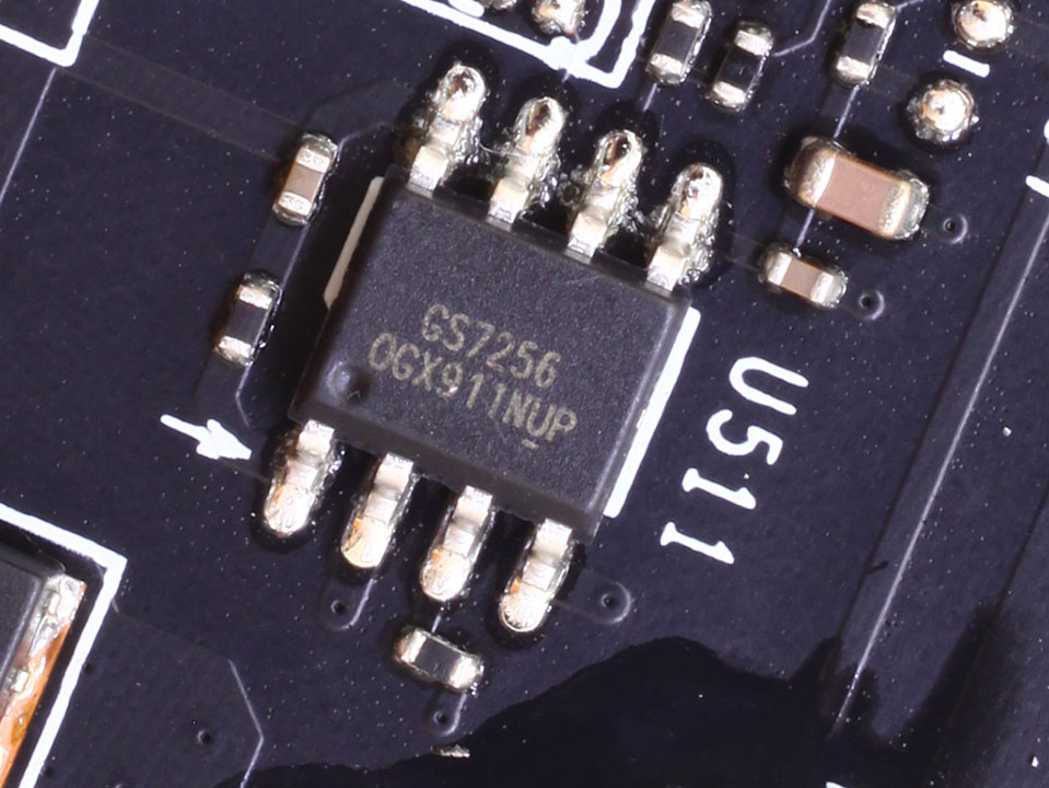
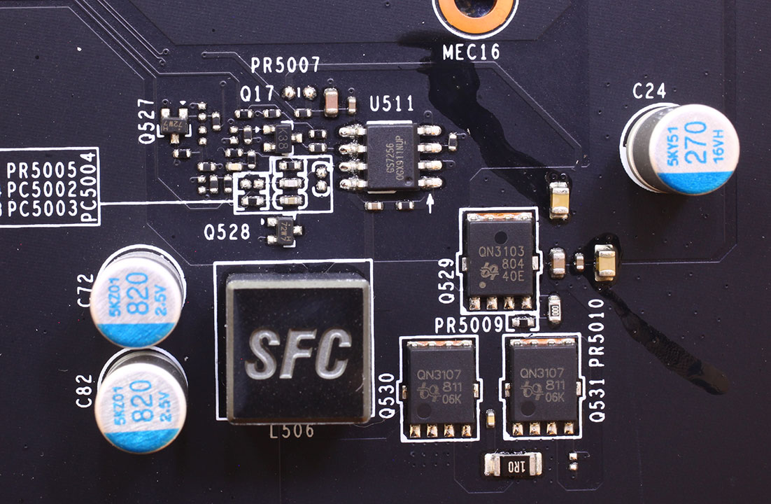
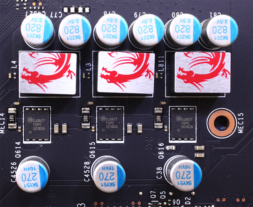
The memory VRM is single-phase, managed by a GS7256 controller.
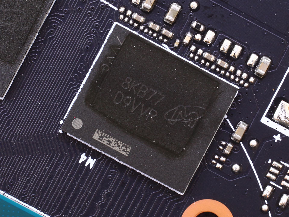
The GDDR5 memory chips are made by Micron and carry the model number D9VVR, which decodes to MT51J256M32HF-80:B. They are specified to run at 2000 MHz (8 Gbps GDDR5 effective).
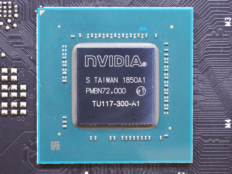
NVIDIA's TU117 graphics processor is the company's smallest chip using the Turing architecture. It is produced on a 12 nm process at TSMC, Taiwan with a die size of 200 mm² and packs 4.70 billion transistors.
May 5th, 2025 19:12 EDT
change timezone
Latest GPU Drivers
New Forum Posts
- EXTREMEHW Invites TECHPOWERUP to our 3RD ANNUAL 96-HOUR FOLDING CHALLENGE April 26th 00:00 UTC (7)
- What's your latest tech purchase? (23709)
- WD Black or Gold for Gaming (10TB) (38)
- Folding Pie and Milestones!! (9498)
- Graphics card..Need help. New to pc. 3070 (43)
- Post Your TIMESPY, PCMARK10 & FIRESTRIKE SCORES! (2019) (310)
- What phone you use as your daily driver? And, a discussion of them. (1684)
- Game Soundtracks You Love (1054)
- Request for advice [Big Build] (60)
- I tried to use AMD Auto Overclock, and now my PC has been freezing up sometimes. Afterwards, the screen goes black or displays artifacts. (34)
Popular Reviews
- ASUS ROG Maximus Z890 Hero Review
- ASUS Radeon RX 9070 XT TUF OC Review
- Clair Obscur: Expedition 33 Performance Benchmark Review - 33 GPUs Tested
- Arctic Liquid Freezer III Pro 360 A-RGB Review
- Montech HS02 PRO Review
- Seasonic Vertex GX 850 W Review
- NVIDIA GeForce RTX 5060 Ti 8 GB Review - So Many Compromises
- Upcoming Hardware Launches 2025 (Updated Apr 2025)
- ASUS GeForce RTX 5090 Astral Liquid OC Review - The Most Expensive GPU I've Ever Tested
- Sapphire Radeon RX 9070 XT Nitro+ Review - Beating NVIDIA
Controversial News Posts
- AMD Radeon RX 9060 XT to Roll Out 8 GB GDDR6 Edition, Despite Rumors (131)
- NVIDIA Sends MSRP Numbers to Partners: GeForce RTX 5060 Ti 8 GB at $379, RTX 5060 Ti 16 GB at $429 (128)
- NVIDIA Launches GeForce RTX 5060 Series, Beginning with RTX 5060 Ti This Week (115)
- Nintendo Confirms That Switch 2 Joy-Cons Will Not Utilize Hall Effect Stick Technology (105)
- NVIDIA PhysX and Flow Made Fully Open-Source (95)
- Sony Increases the PS5 Pricing in EMEA and ANZ by Around 25 Percent (84)
- Parts of NVIDIA GeForce RTX 50 Series GPU PCB Reach Over 100°C: Report (78)
- Intel "Bartlett Lake-S" Gaming CPU is Possible, More Hints Appear for a 12 P-Core SKU (77)