 43
43
MSI GeForce RTX 2070 Super Gaming X Trio Review
(43 Comments) »Introduction
NVIDIA stirred up the graphics card market last week with the debut of its GeForce RTX Super family of graphics cards that increase performance at existing price points in a bid to preempt AMD's Radeon RX 5700-series "Navi" graphics cards. The first two of three RTX Super-series SKUs are the RTX 2060 Super and the RTX 2070 Super. NVIDIA displaced the RTX 2070 from its $499 price point with the better-endowed RTX 2070 Super as AMD beat the RTX 2070 at $399.
The most interesting aspect about the RTX 2070 Super is that it's based on the 13.6 billion-transistor "TU104" silicon since NVIDIA had maxed out the "TU106" with the original RTX 2070. The "TU104" is at the heart of the much pricier RTX 2080 and upcoming RTX 2080 Super graphics cards. What this means to consumers is that most custom-design add-in card (AIC) partners would rather reuse their existing RTX 2080 board designs with a little cost-cutting on the VRM instead of spending money on developing and validating new PCBs. Another benefit is partners using heavy cooling solutions that were originally designed to handle the much hotter RTX 2080, and perhaps even the RTX 2080 Ti.

NVIDIA carved the RTX 2070 Super out of the "TU104" silicon by disabling an entire GPC worth of CUDA cores, leaving the chip with 2,560 out of its 3,072 CUDA cores enabled, besides 160 TMUs, 64 ROPs, 320 Tensor cores, and 40 RT cores. The memory subsystem is untouched. 8 GB of memory ticks at 14 Gbps and sits across a 256-bit wide GDDR6 memory interface, churning out 448 GB/s of memory bandwidth. The GPU clock speeds are increased, too, with up to 1770 MHz GPU Boost frequency, compared to 1620 MHz on the original RTX 2070. Another neat little perk of being based on the "TU104" silicon is NVLink support, which enables 2-way SLI.
In this review, we have with us the MSI GeForce RTX 2070 Super Gaming X Trio, the company's top RTX 2070 Super product. Being based on the larger "TU104" silicon has its perks as board partners prefer reusing RTX 2080 board designs with a few disabled power phases over designing new boards from scratch. The biggest dividend of this is the cooler. You get a gargantuan MSI TriFrozr cooling solution that was originally designed for the rigors of cooling not just the RTX 2080, but also the top-dog RTX 2080 Ti. Besides the GPU, all that sets this card apart from the RTX 2080 Gaming X Trio are a couple of disabled power phases. The card ships with a factory overclock of 1800 MHz GPU Boost, compared to the 1770 MHz reference frequency. It sells at $515, which is only a $15 premium over the $499 MSRP for the RTX 2070 Super.
Our coverage of the RTX Super Series custom-design launch day includes the following content:
MSI GeForce RTX 2060 Super Gaming X | Palit GeForce RTX 2060 Super JetStream | EVGA GeForce RTX 2060 Super SC Ultra | EVGA GeForce RTX 2070 Super FTW3 Ultra | ASUS ROG Strix RTX 2070 Super OC | MSI GeForce RTX 2070 Super Gaming X Trio
| Price | Shader Units | ROPs | Core Clock | Boost Clock | Memory Clock | GPU | Transistors | Memory | |
|---|---|---|---|---|---|---|---|---|---|
| GTX 1080 | $500 | 2560 | 64 | 1607 MHz | 1733 MHz | 1251 MHz | GP104 | 7200M | 8 GB, GDDR5X, 256-bit |
| RTX 2060 Super | $400 | 2176 | 64 | 1470 MHz | 1650 MHz | 1750 MHz | TU106 | 10800M | 8 GB, GDDR6, 256-bit |
| RX 5700 | $350 | 2304 | 64 | 1465 MHz | 1625 MHz | 1750 MHz | Navi 10 | 10300M | 8 GB, GDDR6, 256-bit |
| RX Vega 64 | $500 | 4096 | 64 | 1247 MHz | 1546 MHz | 953 MHz | Vega 10 | 12500M | 8 GB, HBM2, 2048-bit |
| GTX 1080 Ti | $700 | 3584 | 88 | 1481 MHz | 1582 MHz | 1376 MHz | GP102 | 12000M | 11 GB, GDDR5X, 352-bit |
| RTX 2070 | $480 | 2304 | 64 | 1410 MHz | 1620 MHz | 1750 MHz | TU106 | 10800M | 8 GB, GDDR6, 256-bit |
| RX 5700 XT | $400 | 2560 | 64 | 1605 MHz | 1755 MHz | 1750 MHz | Navi 10 | 10300M | 8 GB, GDDR6, 256-bit |
| RTX 2070 Super | $500 | 2560 | 64 | 1605 MHz | 1770 MHz | 1750 MHz | TU104 | 13600M | 8 GB, GDDR6, 256-bit |
| MSI RTX 2070 Super Gaming X Trio | $515 | 2560 | 64 | 1605 MHz | 1800 MHz | 1750 MHz | TU104 | 13600M | 8 GB, GDDR6, 256-bit |
| Radeon VII | $680 | 3840 | 64 | 1802 MHz | N/A | 1000 MHz | Vega 20 | 13230M | 16 GB, HBM2, 4096-bit |
| RTX 2080 | $700 | 2944 | 64 | 1515 MHz | 1710 MHz | 1750 MHz | TU104 | 13600M | 8 GB, GDDR6, 256-bit |
| RTX 2080 Super | $700 | 3072 | 64 | 1650 MHz | 1815 MHz | 1940 MHz | TU104 | 13600M | 8 GB, GDDR6, 256-bit |
| RTX 2080 Ti | $1100 | 4352 | 64 | 1350 MHz | 1545 MHz | 1750 MHz | TU102 | 18600M | 11 GB, GDDR6, 352-bit |
Packaging and Contents


You will receive:
- Graphics card
- Documentation
- Anti-sagging reinforcement brace
- Driver disc
The Card

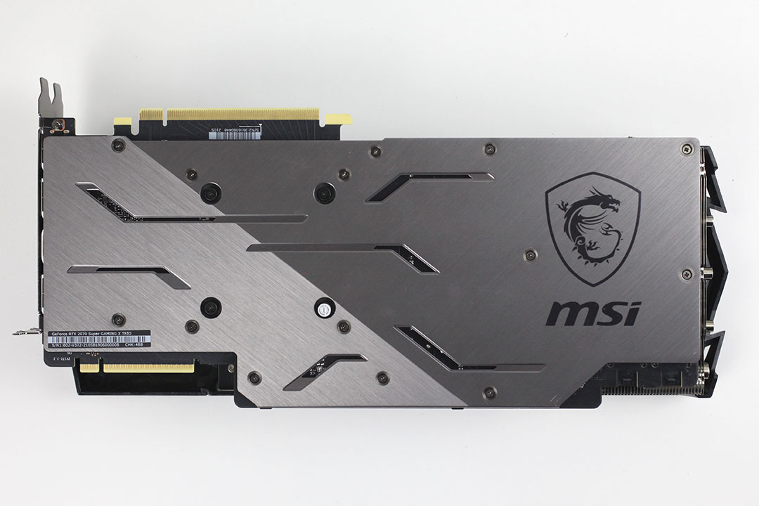
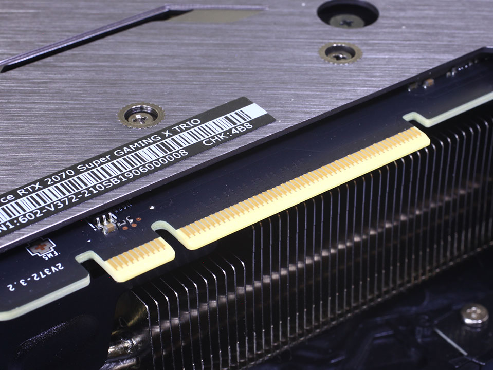
The MSI RTX 2070 Super Gaming X Trio looks identical to the RTX 2080 Gaming X Trio, which of course makes economical sense. On the back, you'll find a high-quality metal backplate. Dimensions of the card are 33x14 cm.

Installation requires three slots in your system.

Display connectivity options include three standard DisplayPort 1.4a and an HDMI 2.0b. Compared to the Founders Edition, the USB-C connector has been removed, probably to reduce cost.
NVIDIA has updated their display engine with the Turing microarchitecture, which now supports DisplayPort 1.4a with support for VESA's nearly lossless Display Stream Compression (DSC). Combined, this enables support for 8K@30Hz with a single cable or 8K@60Hz when DSC is turned on. For context, DisplayPort 1.4a is the latest version of the standard that was published in April, 2018.
At CES 2019, NVIDIA announced that all their graphics cards will now support VESA Adaptive Sync (aka FreeSync). While only a small number of FreeSync monitors have been fully qualified with G-SYNC, users can enable the feature in NVIDIA's control panel regardless of whether the monitor is certified or not.

The board uses two 8-pin power connectors. This input configuration is specified for up to 375 watts of power draw.
With Turing, NVIDIA is using NVLink as a physical layer for its next-generation SLI technology. NVLink provides sufficient bandwidth for multi-GPU rendering at 8K 60 Hz, 4K 120 Hz, and other such bandwidth-heavy display resolutions. It's a point-to-point link between your GPUs, so latencies will be lower compared to pushing data through the PCI-Express bus.
Disassembly


MSI is using a complex dual aluminium fin-stack cooler design that draws heat from the GPU through six heat pipes and is ventilated by three fans.
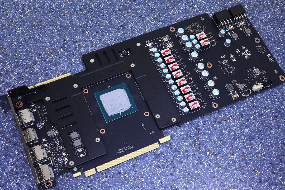
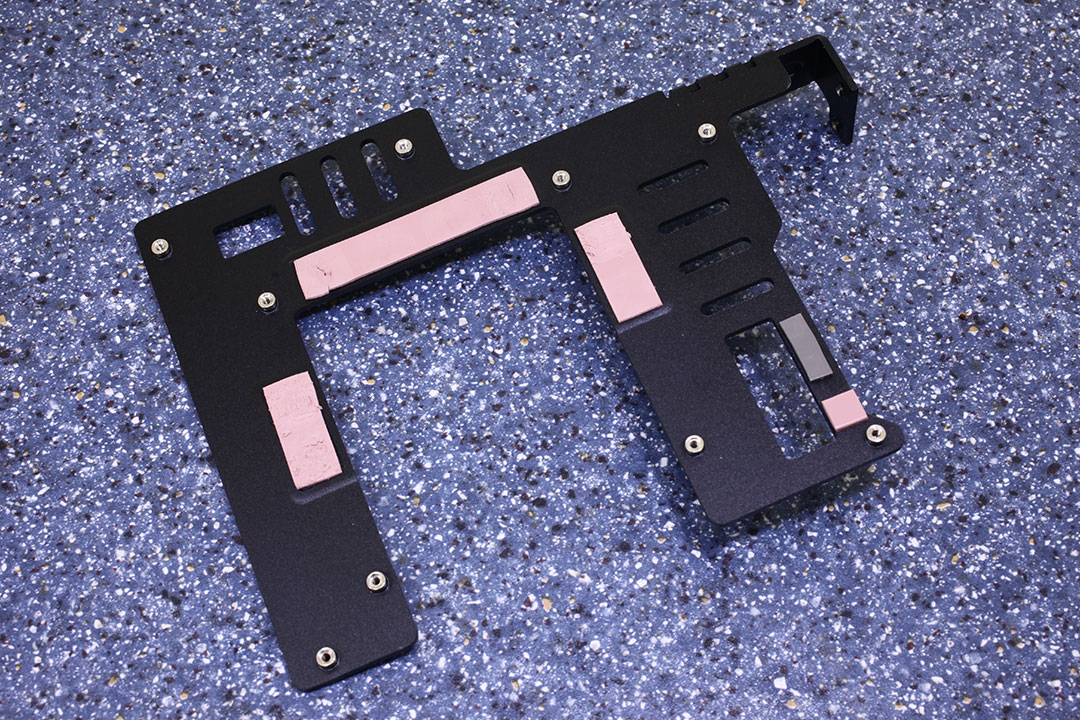
Once the main heatsink is removed, a black baseplate becomes visible, which provides cooling for part of the VRM circuitry and memory chips.
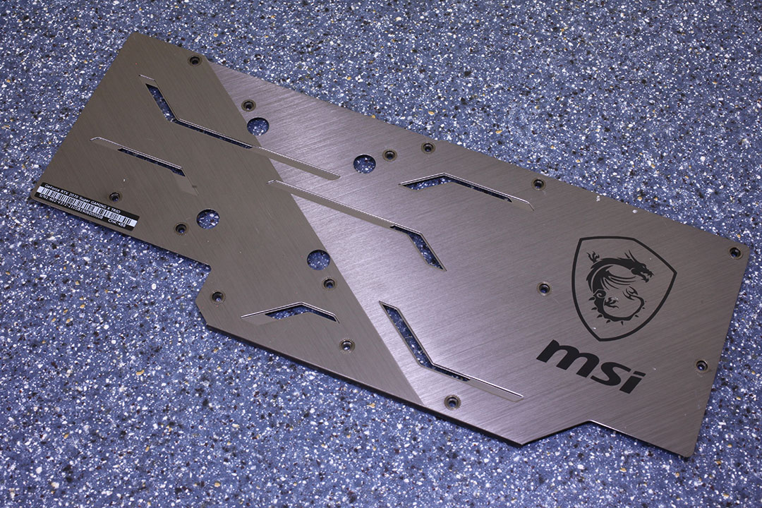
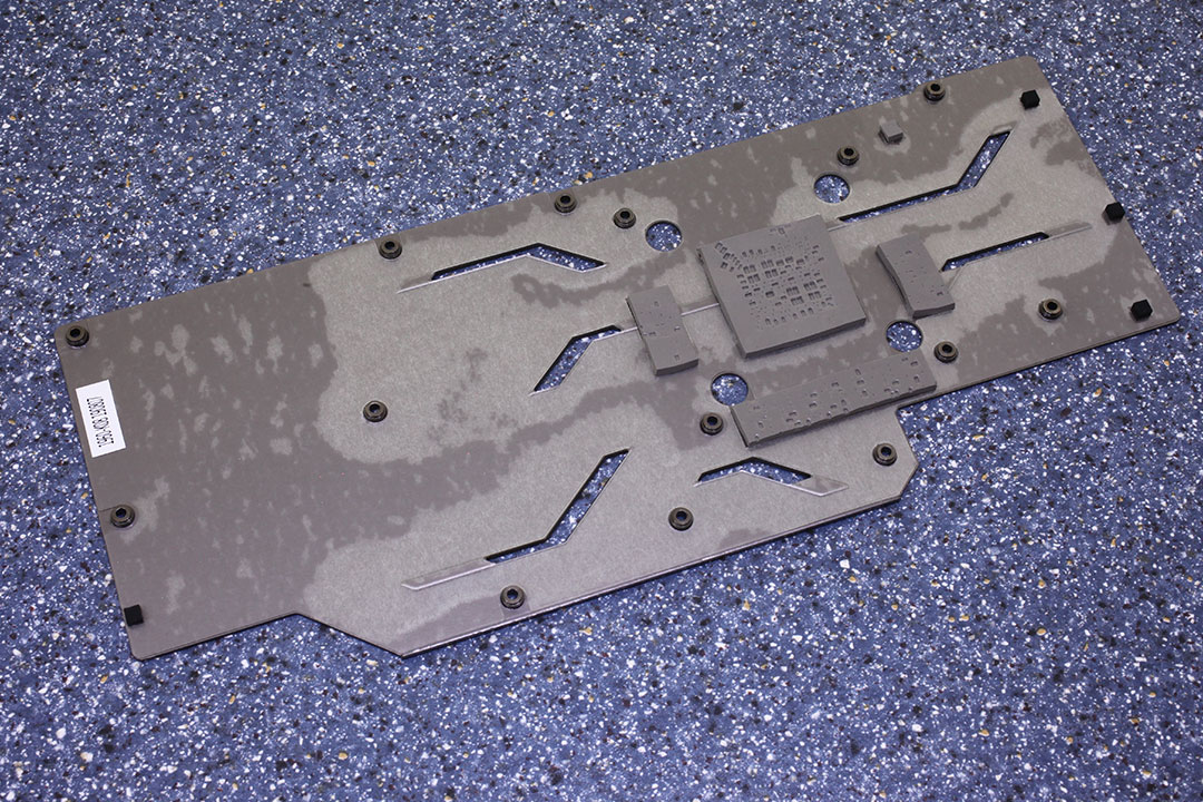
The backplate is made out of metal and protects the card against damage during installation and handling.
On the next page, we dive deep into the PCB layout and VRM configuration.
High-resolution PCB Pictures
These pictures are for the convenience of volt-modders and people who would like to see all the finer details on the PCB. Feel free to link back to us and use them in your articles or forum posts.

High-res versions are also available (front, back).
Our Patreon Silver Supporters can read articles in single-page format.
Apr 11th, 2025 04:37 EDT
change timezone
Latest GPU Drivers
New Forum Posts
- How is the Gainward Phoenix Model in terms of quality? (19)
- Looking for input on fan placement for my Define R5 (18)
- RX 9000 series GPU Owners Club (284)
- The TPU UK Clubhouse (26080)
- 9070XT or 7900XT or 7900XTX (185)
- GALAX GeForce RTX 4090 SG 1-Click OC (8)
- Your PC ATM (35343)
- Bios RX 570 (10)
- TPU's Nostalgic Hardware Club (20222)
- Lossless scaling (8)
Popular Reviews
- The Last Of Us Part 2 Performance Benchmark Review - 30 GPUs Compared
- ASRock Z890 Taichi OCF Review
- Thermaltake TR100 Review
- Zotac GeForce RTX 5070 Ti Amp Extreme Review
- Sapphire Radeon RX 9070 XT Pulse Review
- Acer Predator GM9000 2 TB Review
- Sapphire Radeon RX 9070 XT Nitro+ Review - Beating NVIDIA
- Upcoming Hardware Launches 2025 (Updated Apr 2025)
- PowerColor Radeon RX 9070 Hellhound Review
- MCHOSE L7 Pro Review
Controversial News Posts
- NVIDIA GeForce RTX 5060 Ti 16 GB SKU Likely Launching at $499, According to Supply Chain Leak (179)
- MSI Doesn't Plan Radeon RX 9000 Series GPUs, Skips AMD RDNA 4 Generation Entirely (146)
- Microsoft Introduces Copilot for Gaming (124)
- AMD Radeon RX 9070 XT Reportedly Outperforms RTX 5080 Through Undervolting (119)
- NVIDIA Reportedly Prepares GeForce RTX 5060 and RTX 5060 Ti Unveil Tomorrow (115)
- NVIDIA Sends MSRP Numbers to Partners: GeForce RTX 5060 Ti 8 GB at $379, RTX 5060 Ti 16 GB at $429 (110)
- Nintendo Confirms That Switch 2 Joy-Cons Will Not Utilize Hall Effect Stick Technology (103)
- Over 200,000 Sold Radeon RX 9070 and RX 9070 XT GPUs? AMD Says No Number was Given (100)