 8
8
MSI GeForce RTX 2070 Super Gaming X Review
(8 Comments) »Introduction
NVIDIA stirred up the graphics card market this summer with the debut of its GeForce RTX Super family of graphics cards that increase performance at existing price points in a bid to preempt AMD's Radeon RX 5700-series "Navi" graphics cards. The first two of three RTX Super-series SKUs are the RTX 2060 Super and the RTX 2070 Super. NVIDIA displaced the RTX 2070 from its $499 price point with the better-endowed RTX 2070 Super as AMD beat the RTX 2070 at $399.
The most interesting aspect about the RTX 2070 Super is that it's based on the 13.6 billion-transistor "TU104" silicon since NVIDIA had maxed out the "TU106" with the original RTX 2070. The "TU104" is at the heart of the much pricier RTX 2080 and upcoming RTX 2080 Super graphics cards. What this means to consumers is that most custom-design add-in card (AIC) partners would rather reuse their existing RTX 2080 board designs with a little cost-cutting on the VRM instead of spending money on developing and validating new PCBs. Another benefit is partners using heavy cooling solutions that were originally designed to handle the much hotter RTX 2080, and perhaps even the RTX 2080 Ti.

NVIDIA carved the RTX 2070 Super out of the "TU104" silicon by disabling an entire GPC worth of CUDA cores, leaving the chip with 2,560 out of its 3,072 CUDA cores enabled, besides 160 TMUs, 64 ROPs, 320 Tensor cores, and 40 RT cores. The memory subsystem is untouched. 8 GB of memory ticks at 14 Gbps and sits across a 256-bit wide GDDR6 memory interface, churning out 448 GB/s of memory bandwidth. The GPU clock speeds are increased, too, with up to 1770 MHz GPU Boost frequency, compared to 1620 MHz on the original RTX 2070. Another neat little perk of being based on the "TU104" silicon is NVLink support, which enables 2-way SLI.
In this review, we have with us the MSI GeForce RTX 2070 Super Gaming X. This is MSI's second kind of "Gaming X" product based on the RTX 2070 Super, the other being the Gaming X Trio (which we reviewed here). The card uses a slightly more compact Twin Frozr 7 cooling solution that comes with two large fans, as opposed to three fans on the Gaming X Trio. The underlying PCB is also a bit more compact, but uses the same 8+2 VRM configuration. The card comes with the same exact factory-overclock and power-limits as the Gaming X Trio, with 1800 MHz maximum GPU Boost, and an untouched 14 Gbps GDDR6 memory. You get essentials such as idle fan-stop, and a ton of RGB LED embellishments. MSI plans to sell the RTX 2070 Super Gaming X at a price of $510, a mere $10 premium over the $499 NVIDIA baseline price.
| Price | Shader Units | ROPs | Core Clock | Boost Clock | Memory Clock | GPU | Transistors | Memory | |
|---|---|---|---|---|---|---|---|---|---|
| GTX 1080 | $500 | 2560 | 64 | 1607 MHz | 1733 MHz | 1251 MHz | GP104 | 7200M | 8 GB, GDDR5X, 256-bit |
| RTX 2060 Super | $400 | 2176 | 64 | 1470 MHz | 1650 MHz | 1750 MHz | TU106 | 10800M | 8 GB, GDDR6, 256-bit |
| RX 5700 | $350 | 2304 | 64 | 1465 MHz | 1625 MHz | 1750 MHz | Navi 10 | 10300M | 8 GB, GDDR6, 256-bit |
| RX Vega 64 | $500 | 4096 | 64 | 1247 MHz | 1546 MHz | 953 MHz | Vega 10 | 12500M | 8 GB, HBM2, 2048-bit |
| GTX 1080 Ti | $700 | 3584 | 88 | 1481 MHz | 1582 MHz | 1376 MHz | GP102 | 12000M | 11 GB, GDDR5X, 352-bit |
| RTX 2070 | $480 | 2304 | 64 | 1410 MHz | 1620 MHz | 1750 MHz | TU106 | 10800M | 8 GB, GDDR6, 256-bit |
| RX 5700 XT | $400 | 2560 | 64 | 1605 MHz | 1755 MHz | 1750 MHz | Navi 10 | 10300M | 8 GB, GDDR6, 256-bit |
| RTX 2070 Super | $500 | 2560 | 64 | 1605 MHz | 1770 MHz | 1750 MHz | TU104 | 13600M | 8 GB, GDDR6, 256-bit |
| MSI RTX 2070 Super Gaming X | $510 | 2560 | 64 | 1605 MHz | 1800 MHz | 1750 MHz | TU104 | 13600M | 8 GB, GDDR6, 256-bit |
| Radeon VII | $680 | 3840 | 64 | 1802 MHz | N/A | 1000 MHz | Vega 20 | 13230M | 16 GB, HBM2, 4096-bit |
| RTX 2080 | $700 | 2944 | 64 | 1515 MHz | 1710 MHz | 1750 MHz | TU104 | 13600M | 8 GB, GDDR6, 256-bit |
| RTX 2080 Super | $700 | 3072 | 64 | 1650 MHz | 1815 MHz | 1940 MHz | TU104 | 13600M | 8 GB, GDDR6, 256-bit |
| RTX 2080 Ti | $1100 | 4352 | 64 | 1350 MHz | 1545 MHz | 1750 MHz | TU102 | 18600M | 11 GB, GDDR6, 352-bit |
Packaging and Contents
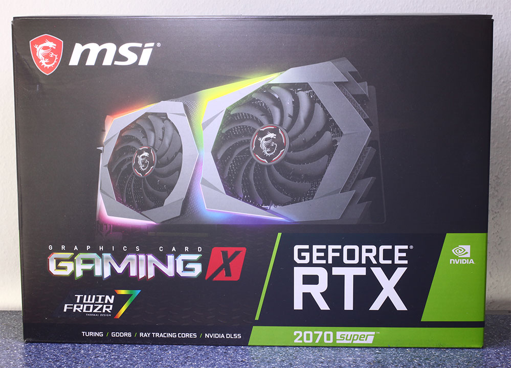

You will receive:
- Graphics card
- Documentation
- Graphics card reinforcement brace (forgot to include it in the picture)
The Card


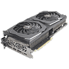
MSI has created a new design for the Gaming X that is very similar to that of the Gaming X Trio. The dominant colors are black and gray, with a high-quality metal backplate on the back in matching colors. Dimensions of the card are 30.0 x 14.5 cm. This makes the card 3 cm shorter than the Gaming X Trio.
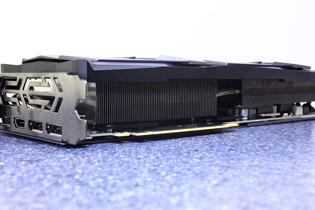

Installation requires three slots in your system.

Display connectivity options include three standard DisplayPort 1.4a and an HDMI 2.0b. Compared to the Founders Edition, the USB-C connector has been removed, probably to reduce cost.
NVIDIA has updated their display engine with the Turing microarchitecture, which now supports DisplayPort 1.4a with support for VESA's nearly lossless Display Stream Compression (DSC). Combined, this enables support for 8K@30Hz with a single cable or 8K@60Hz when DSC is turned on. For context, DisplayPort 1.4a is the latest version of the standard that was published in April, 2018.
At CES 2019, NVIDIA announced that all their graphics cards will now support VESA Adaptive Sync (aka FreeSync). While only a small number of FreeSync monitors have been fully qualified with G-SYNC, users can enable the feature in NVIDIA's control panel regardless of whether the monitor is certified or not.

The board uses one 6-pin and one 8-pin power connector. This input configuration is specified for up to 300 watts of power draw.

With Turing, NVIDIA is using NVLink as a physical layer for its next-generation SLI technology. NVLink provides sufficient bandwidth for multi-GPU rendering at 8K 60 Hz, 4K 120 Hz, and other such bandwidth-heavy display resolutions. It's a point-to-point link between your GPUs, so latencies will be lower compared to pushing data through the PCI-Express bus.
Disassembly


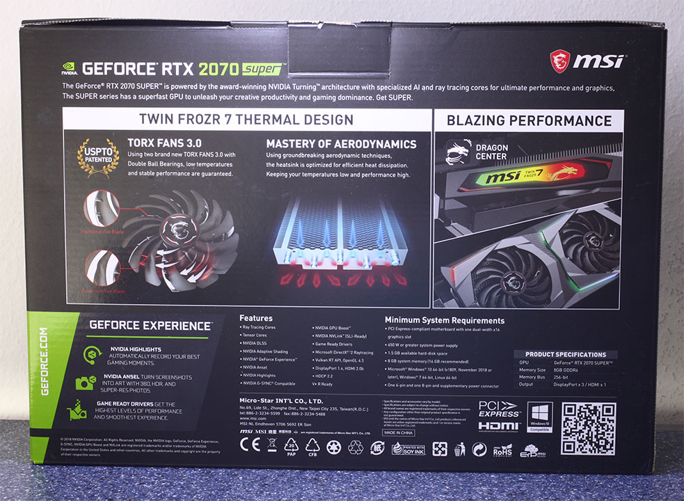
MSI is using an elaborate system of six heatpipes on their cooler (the Gaming X Trio uses seven).

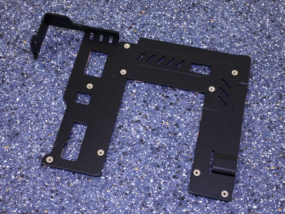
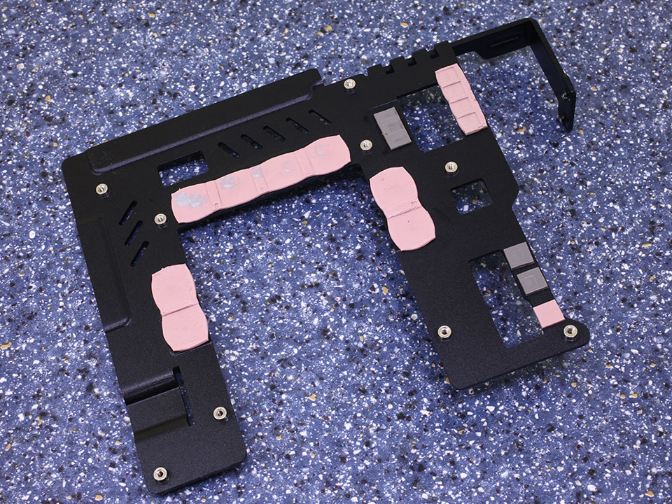
Once the main heatsink is removed, a black baseplate becomes visible, which provides cooling for part of the VRM circuitry and memory chips.
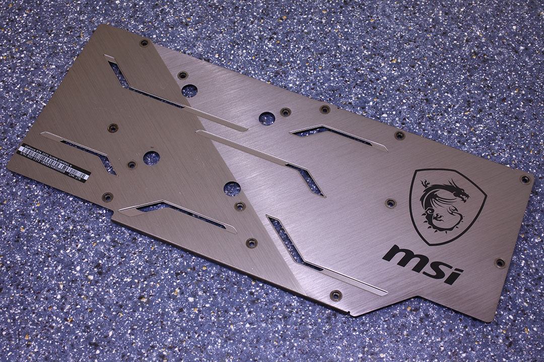
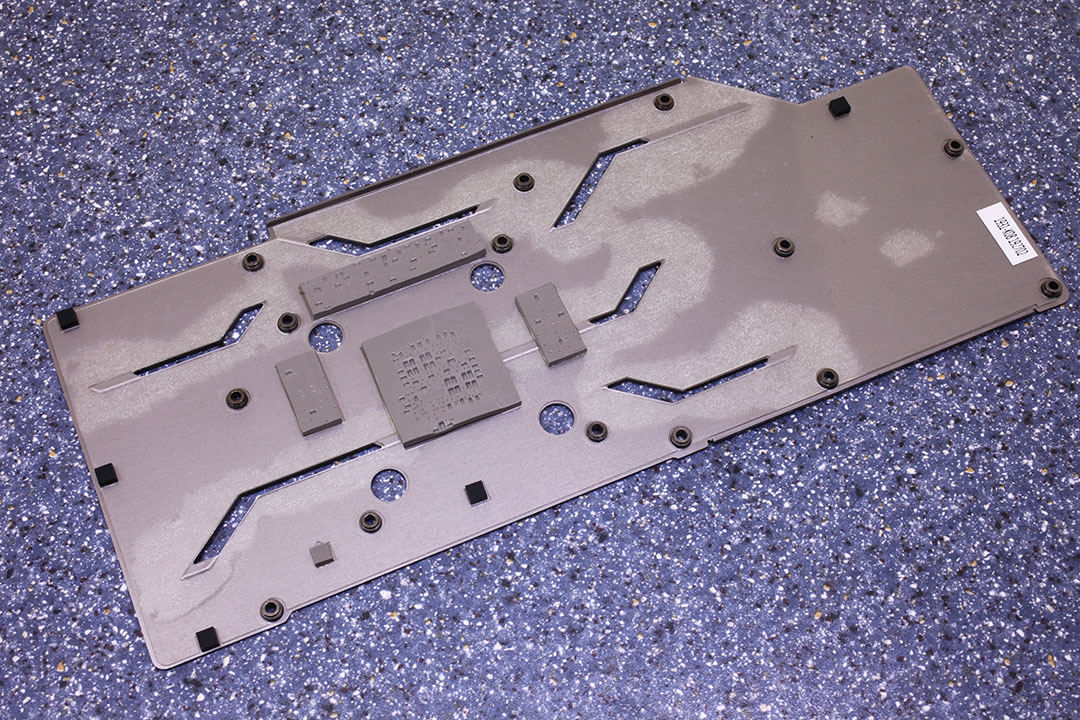
The backplate is made out of metal and protects the card against damage during installation and handling.
On the next page, we dive deep into the PCB layout and VRM configuration.
High-resolution PCB Pictures
These pictures are for the convenience of volt-modders and people who would like to see all the finer details on the PCB. Feel free to link back to us and use them in your articles or forum posts.
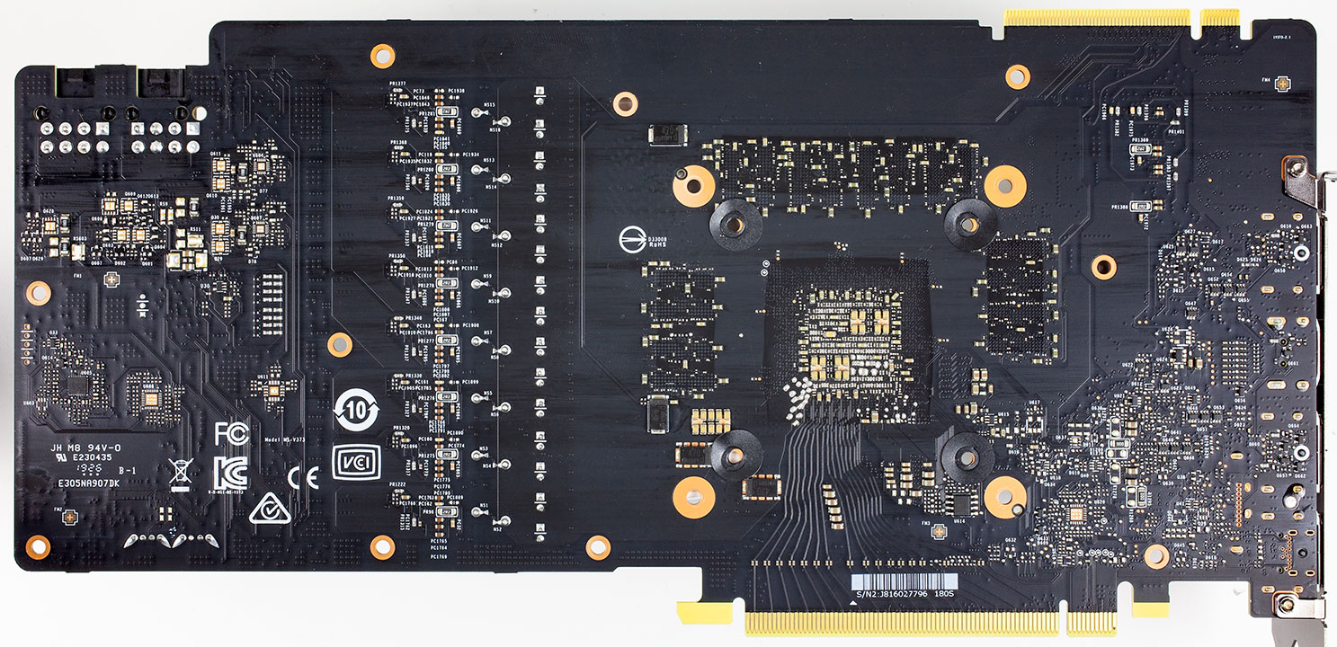
High-res versions are also available (front, back).
Our Patreon Silver Supporters can read articles in single-page format.
May 6th, 2025 19:47 EDT
change timezone
Latest GPU Drivers
New Forum Posts
- Do you guys have backup GPUs? (109)
- Ryzen Processor and FIT - understanding v-core to avoid damages. (5)
- What's your latest tech purchase? (23726)
- I can't flash GPU BIOS.“The PCI BAR assignment for the processed device is invalid.” (3)
- Thermal testing two different size Gigabyte 5070 Ti cards - huge differences (32)
- Will you buy a RTX 5090? (493)
- Ssd failure, I don’t know what to do (30)
- How high of a ram frequency can i run on a Z690 with an 14700Kf processor? (13)
- need help choosing a CPU (6)
- MSI Vector GP68HX i9 12900HX - How to increase battery life? (3)
Popular Reviews
- Arctic Liquid Freezer III Pro 360 A-RGB Review
- ASUS Radeon RX 9070 XT TUF OC Review
- Clair Obscur: Expedition 33 Performance Benchmark Review - 33 GPUs Tested
- ASUS ROG Maximus Z890 Hero Review
- Zotac GeForce RTX 5070 Ti Amp Extreme Review
- Upcoming Hardware Launches 2025 (Updated Apr 2025)
- Seasonic Vertex GX 850 W Review
- Sapphire Radeon RX 9070 XT Nitro+ Review - Beating NVIDIA
- ASUS GeForce RTX 5090 Astral Liquid OC Review - The Most Expensive GPU I've Ever Tested
- AMD Ryzen 7 9800X3D Review - The Best Gaming Processor
Controversial News Posts
- AMD Radeon RX 9060 XT to Roll Out 8 GB GDDR6 Edition, Despite Rumors (142)
- NVIDIA Sends MSRP Numbers to Partners: GeForce RTX 5060 Ti 8 GB at $379, RTX 5060 Ti 16 GB at $429 (128)
- NVIDIA Launches GeForce RTX 5060 Series, Beginning with RTX 5060 Ti This Week (115)
- Nintendo Confirms That Switch 2 Joy-Cons Will Not Utilize Hall Effect Stick Technology (105)
- Sony Increases the PS5 Pricing in EMEA and ANZ by Around 25 Percent (84)
- Parts of NVIDIA GeForce RTX 50 Series GPU PCB Reach Over 100°C: Report (78)
- Intel "Bartlett Lake-S" Gaming CPU is Possible, More Hints Appear for a 12 P-Core SKU (77)
- China Develops HDMI Alternative: 192 Gbps Speeds and 480 W Power Delivery (74)