 14
14
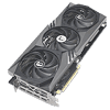
MSI GeForce RTX 4070 Gaming X Trio Review
Test Setup »High-resolution PCB Pictures
These pictures are for the convenience of volt modders and people who would like to see all the finer details on the PCB. Feel free to link back to us and use these in your articles, videos or forum posts.High-resolution versions are also available (front, back).
Circuit Board (PCB) Analysis
GPU voltage is a nine-phase design, managed by a uPI uP9512R controller.
Alpha & Omega AOZ5311NQI BLN3 DrMOS components are used for GPU voltage; they are rated for 55 A of current each.
Memory voltage is a two-phase design, managed by a uPI uP9529Q controller.
For memory, Alpha & Omega AOZ5311NQI BLN30 are used, too, with a 55 A rating.
The GDDR6X memory chips are made by Micron and carry the model number D8BZC, which decodes to MT61K512M32KPA-21:U. They are specified to run at 1313 MHz (21 Gbps GDDR6 effective).
NVIDIA's AD104 graphics processor is the company's third Ada Lovelace GPU. It is built using a 5 nanometer process at TSMC Taiwan, with a transistor count of 35.8 billion and a die size of 295 mm².
Feb 12th, 2025 17:30 EST
change timezone
Latest GPU Drivers
New Forum Posts
- What is the point of 9800X3D in 4k? Isn't 9950X better at the same price? (67)
- Voxtar Hp58 wireless thermal printer (1)
- camper van computer (19)
- Monitor Battle! Help me choose between two contenders (22)
- Monster Hunter WIlds - CPU scores (4)
- Were Ryzen 8000 CPUs a big mistake from AMD? (26)
- [Testers-Needed] Converting Any Realtek Ethernet to Intel Killer Ethernet chip (85)
- Windows 11 performance mode (0)
- win10 or win11 (16)
- Proposed new Power Connector (43)
Popular Reviews
- Civilization VII Performance Benchmark Review - 35 GPUs Tested
- Kingdom Come Deliverance II Performance Benchmark Review - 35 GPUs Tested
- Team Group T-Force XTREEM DDR5-7200 48GB CL34 Review
- ASRock Phantom Gaming B850I Lightning Wi-Fi Review
- DAREU A980 Pro Max Review
- AMD Ryzen 7 9800X3D Review - The Best Gaming Processor
- NVIDIA GeForce RTX 5080 Founders Edition Review
- WD Black SN7100 2 TB Review - The New Best SSD
- Corsair Frame 4000D Review
- Spider-Man 2 Performance Benchmark Review - 35 GPUs Tested
Controversial News Posts
- AMD Radeon 9070 XT Rumored to Outpace RTX 5070 Ti by Almost 15% (296)
- AMD is Taking Time with Radeon RX 9000 to Optimize Software and FSR 4 (256)
- Edward Snowden Lashes Out at NVIDIA Over GeForce RTX 50 Pricing And Value (241)
- AMD Denies Radeon RX 9070 XT $899 USD Starting Price Point Rumors (239)
- AMD Radeon RX 9070 XT & RX 9070 Custom Models In Stock at European Stores (226)
- New Leak Reveals NVIDIA RTX 5080 Is Slower Than RTX 4090 (215)
- AMD's Radeon RX 9070 Launch Faces Pricing Hurdles (175)
- AMD Radeon RX 9070 XT Launch Allegedly Set for March 6 (152)


