 16
16
MSI GeForce RTX 5080 Vanguard SOC Review
(16 Comments) »Introduction
MSI debuts its new Vanguard line of graphics cards with the GeForce RTX 50-series, and we have with us the MSI RTX 5080 Vanguard SOC graphics card, in its Launch Edition collector's package. The new Vanguard line of graphics cards are positioned between MSI's SUPRIM line of halo-segment custom design graphics cards, and its more popular Gaming X series. The company retired the Gaming Z series with the advent of SUPRIM, so I guess you could call Vanguard the spiritual successor to the Gaming Z. The MSI Vanguard series combines aspects of both SUPRIM and Gaming X. From the SUPRIM you see hints of titanium gray metal alloy embellishments on the cooler shroud. The backplate has a matching brushed-aluminium appearance, and from the Gaming X series, it has certain sporty elements, such as carbon fiber surfaces and acrylic RGB LED lighting diffusers. Under the shroud, the Vanguard features many of the cooler innovations MSI introduced with the SUPRIM series this generation.

The GeForce RTX 5080 is NVIDIA's latest enthusiast-segment graphics card, designed for maxed out gaming at 4K Ultra HD, with ray tracing enabled. The flagship RTX 5090 from last week does the same thing, but faster, and has other use cases such as AI development and content creation, thanks to its much larger video memory and memory bus. The RTX 5080 squarely targets gamers looking for a 4K gaming experience, with a few allied workloads on the side, such as game streaming. If compare the specs sheets of the RTX 5090 and RTX 5080, you'll find that the latter is almost half the card the RTX 5090 is, and is yet squarely an enthusiast-segment GPU. The RTX 5080 debuts the new GB203 silicon, which is the second largest to implement the GeForce Blackwell graphics architecture. With this generation, NVIDIA is holding on to the process node, so these chips are built on the same NVIDIA 4N silicon fabrication node that the company codeveloped with TSMC, based on the foundry's 5 nm EUV node.
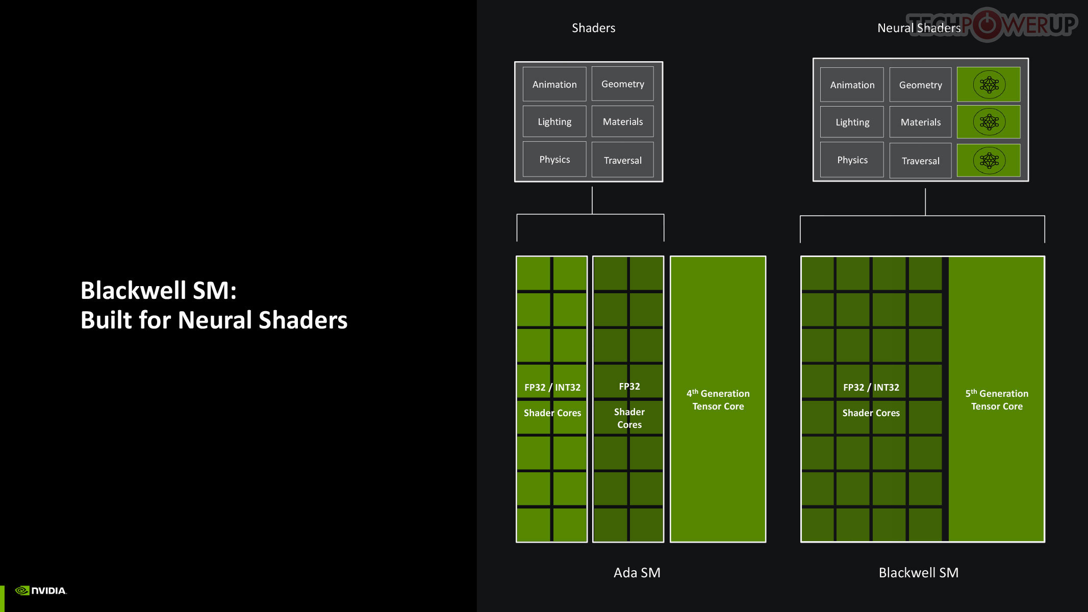
The GeForce Blackwell graphics architecture introduces a revolutionary new concept in consumer 3D graphics, called Neural Rendering. The company figured out a way to combine objects created by a generative AI with conventional raster 3D graphics, just like it discovered a way to combine real time ray traced objects with RTX late last decade. You already know the ability of popular generative AI models to create photorealistic images and video, so you know this technology has immense potential. GeForce Blackwell GPUs have the ability to accelerate generative AI and render 3D graphics in tandem, thanks to a new hardware scheduling component called the AI management processor. The architecture also introduces the ability for 3D applications to directly access the Tensor cores, and NVIDIA worked with Microsoft to standardize this at the DirectX API level.
The new Blackwell SM features concurrent FP32 and INT32 capability on all 128 CUDA cores, the previous generation Ada SM only has INT32 capability on half its cores. The 5th Generation Tensor core puts on FP4 data format capability to step up throughput by trading in precision. The 4th Generation RT core has the hardware groundwork for Mega Geometry, letting ray traced objects have exponentially higher polygon counts. DLSS 4 and Multi Frame Generation are this generation's other major highlights. DLSS 4 introduces a new Transformer based AI model replacing the CNN-based one, for all its subcomponents, namely, super resolution, ray reconstruction, and frame generation. This model is more accurate, and hence steps up image quality in every performance tier. Multi Frame Generation gives the GPU the ability to use AI to draw not just one succeeding frame to a conventionally rendered one, but four such succeeding frames, effectively quadrupling frame rate. It relies on the new Flip Metering component of the Blackwell Display Engine to achieve this.
Blackwell implements many technological firsts for the company. It's the first gaming GPU to use the PCI-Express 5.0 x16 host interface, the 12V-2x6 power connector, and feature an ATX 3.1 + PCIe 5 CEM power architecture. It's also the first generation to implement the new GDDR7 memory standard, which doubles efficiency over GDDR6. The Blackwell display engine implements DisplayPort 2.1b with UHBR20 on all ports. When used with DSC, it enables 8K high refresh-rates with a single cable. You can see where this is going with DLSS 4 MFG.
The GeForce RTX 5080 maxes out the GB203 silicon, enabling all 84 SM, which works out to 10,752 CUDA cores, 336 Tensor cores, 84 RT cores, 336 TMUs, and 112 ROPs. It also features all 64 MB of the on-die L2 cache, and two sets of NVDEC and NVENC video accelerators that support 4:2:2 formats for AV1 and HEVC. The chip features a 256-bit wide GDDR7 memory bus, which drives 16 GB of memory. NVIDIA is running this memory at 30 Gbps on the RTX 5080, yielding 960 GB/s of bandwidth—a 34% increase over that of the RTX 4080.
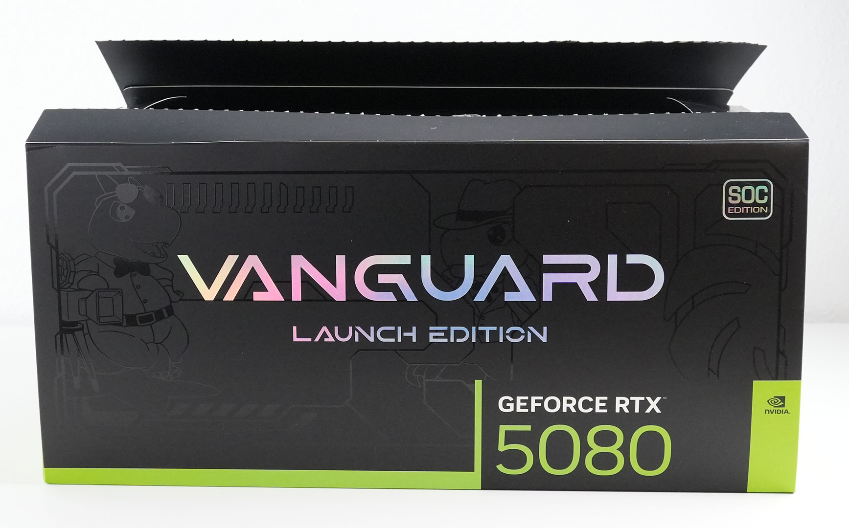
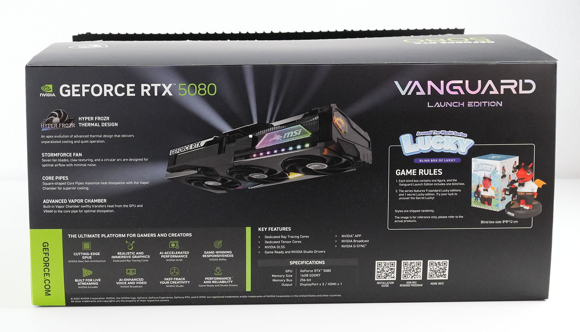
The MSI GeForce RTX 5080 Vanguard SOC, as we said, combines the cooling innovations of the SUPRIM series, with the aesthetics of both the SUPRIM and Gaming X series. The new Hyper Frozr cooling solution comes with a vapor chamber plate making contact with the GPU and memory, which conveys heat to a cluster of heat pipes that have been flattened to a cuboidal shape for better contact with the vapor chamber. From here, the heat is spread across a large aluminium fin-stack with wavy edges that increase turbulence for better heat dissipation. The cooler relies on a trio of MSI's StormForce fans, the same exact ones found in the company's RTX 5080 SUPRIM graphics card which we are also reviewing today. There are two sub-variants of the RTX 5080 Vanguard, SOC and OC, we're reviewing the SOC, which comes with a higher factory overclock of 2730 MHz on both the Gaming and Silent BIOSes, compared to 2617 MHz reference. The Launch Edition is a special package that includes a puzzle toy based on Lucky, MSI's dragon mascot. MSI is pricing this card at $1230, a $230 premium over the $999 baseline.
| Price | Cores | ROPs | Core Clock | Boost Clock | Memory Clock | GPU | Transistors | Memory | |
|---|---|---|---|---|---|---|---|---|---|
| RTX 3080 | $420 | 8704 | 96 | 1440 MHz | 1710 MHz | 1188 MHz | GA102 | 28000M | 10 GB, GDDR6X, 320-bit |
| RTX 4070 | $490 | 5888 | 64 | 1920 MHz | 2475 MHz | 1313 MHz | AD104 | 35800M | 12 GB, GDDR6X, 192-bit |
| RX 7800 XT | $440 | 3840 | 96 | 2124 MHz | 2430 MHz | 2425 MHz | Navi 32 | 28100M | 16 GB, GDDR6, 256-bit |
| RX 6900 XT | $450 | 5120 | 128 | 2015 MHz | 2250 MHz | 2000 MHz | Navi 21 | 26800M | 16 GB, GDDR6, 256-bit |
| RX 6950 XT | $630 | 5120 | 128 | 2100 MHz | 2310 MHz | 2250 MHz | Navi 21 | 26800M | 16 GB, GDDR6, 256-bit |
| RTX 3090 | $900 | 10496 | 112 | 1395 MHz | 1695 MHz | 1219 MHz | GA102 | 28000M | 24 GB, GDDR6X, 384-bit |
| RTX 4070 Super | $590 | 7168 | 80 | 1980 MHz | 2475 MHz | 1313 MHz | AD104 | 35800M | 12 GB, GDDR6X, 192-bit |
| RX 7900 GRE | $530 | 5120 | 160 | 1880 MHz | 2245 MHz | 2250 MHz | Navi 31 | 57700M | 16 GB, GDDR6, 256-bit |
| RTX 4070 Ti | $700 | 7680 | 80 | 2310 MHz | 2610 MHz | 1313 MHz | AD104 | 35800M | 12 GB, GDDR6X, 192-bit |
| RTX 4070 Ti Super | $750 | 8448 | 96 | 2340 MHz | 2610 MHz | 1313 MHz | AD103 | 45900M | 16 GB, GDDR6X, 256-bit |
| RX 7900 XT | $620 | 5376 | 192 | 2000 MHz | 2400 MHz | 2500 MHz | Navi 31 | 57700M | 20 GB, GDDR6, 320-bit |
| RTX 3090 Ti | $1000 | 10752 | 112 | 1560 MHz | 1950 MHz | 1313 MHz | GA102 | 28000M | 24 GB, GDDR6X, 384-bit |
| RTX 4080 | $940 | 9728 | 112 | 2205 MHz | 2505 MHz | 1400 MHz | AD103 | 45900M | 16 GB, GDDR6X, 256-bit |
| RTX 4080 Super | $990 | 10240 | 112 | 2295 MHz | 2550 MHz | 1438 MHz | AD103 | 45900M | 16 GB, GDDR6X, 256-bit |
| RX 7900 XTX | $820 | 6144 | 192 | 2300 MHz | 2500 MHz | 2500 MHz | Navi 31 | 57700M | 24 GB, GDDR6, 384-bit |
| RTX 5080 | $1000 | 10752 | 112 | 2295 MHz | 2617 MHz | 1875 MHz | GB203 | 45600M | 16 GB, GDDR7, 256-bit |
| MSI RTX 5080 Vanguard SOC | $1230 | 10752 | 112 | 2295 MHz | 2730 MHz | 1875 MHz | GB203 | 45600M | 16 GB, GDDR7, 256-bit |
| RTX 4090 | $2400 | 16384 | 176 | 2235 MHz | 2520 MHz | 1313 MHz | AD102 | 76300M | 24 GB, GDDR6X, 384-bit |
| RTX 5090 | $2000 | 21760 | 176 | 2017 MHz | 2407 MHz | 1750 MHz | GB202 | 92200M | 32 GB, GDDR7, 512-bit |
NVIDIA Blackwell Architecture
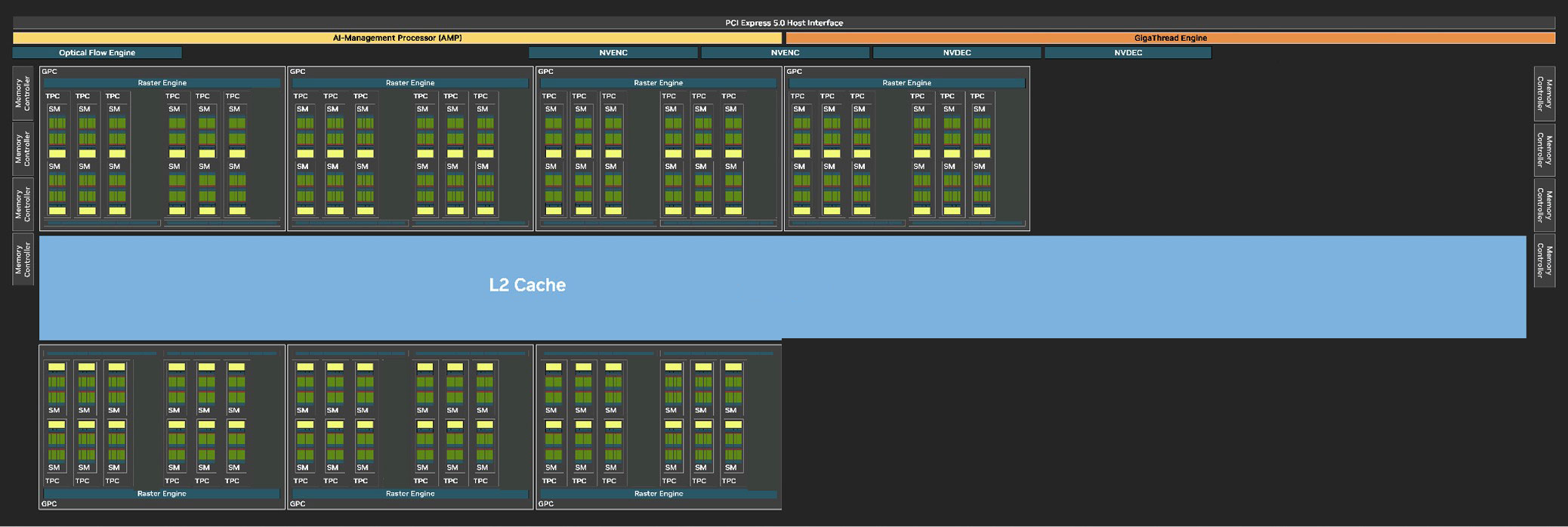
NVIDIA does not provide a block diagram for the GB203 GPU (we asked), so we had to quickly hack one out from the GB202 diagram. This is accurate just not as pretty.
The GeForce Blackwell graphics architecture heralds NVIDIA's 4th generation of RTX, the late-2010s re-invention of the modern GPU that sees a fusion of real time ray traced objects with conventional raster 3D graphics. With Blackwell, NVIDIA is helping add another dimension, neural rendering, the ability for the GPU to leverage a generative AI to create portions of a frame. This is different from DLSS, where an AI model is used to reconstruct details in an upscaled frame based on its training date, temporal frames, and motion vectors. Today we are reviewing NVIDIA's second-biggest silicon from this generation, the RTX 5080. At the heart of this graphics card is the new 5 nm GB203 silicon. This chip has very similar die size and transistor counts to the previous generation AD103 powering the RTX 4080, because both chips are built on the exact same process—TSMC's "NVIDIA 4N", or 5 nm EUV with NVIDIA-specific characteristics—but is based on the newer Blackwell graphics architecture. The GB203 measures 378 mm² in die-area and rocks 45.6 billion transistors (compared to the 378.6 mm² die-area and 45.9 billion transistors of the AD103). This is where the similarities end.
The GB203 silicon is laid out essentially in the same component hierarchy as past generations of NVIDIA GPUs, but with a few notable changes. The GPU features a PCI-Express 5.0 x16 host interface. PCIe Gen 5 has been around since Intel's 12th Gen Core "Alder Lake" and AMD's Ryzen 7000 "Zen 4," so there is a sizable install-base of systems that can take advantage of it. The GPU is of course compatible with older generations of PCIe. The GB203 also features the new GDDR7 memory interface that's making its debut with this generation. The chip features a 256-bit wide memory bus, which is half the bus width of the GB202 powering the RTX 5090. NVIDIA is using this to drive 16 GB of memory at 30 Gbps speeds, yielding 960 GB/s of memory bandwidth, which is a 34% increase over the RTX 4080 and its 22.5 Gbps GDDR6X.
The GigaThread Engine is the main graphics rendering workload allocation logic on the GB203, but there's a new addition, a dedicated serial processor for managing all AI acceleration resources on the GPU, NVIDIA calls this AMP (AI management processor). Other components at the global level are the Optical Flow Processor, a component involved in older versions of DLSS frame generation and for video encoding; and an updated media acceleration engine consisting of two NVENC encode accelerators, and two NVDEC decode accelerators. The new 9th Gen NVENC video encode accelerators come with 4:2:2 AV1 and HEVC encoding support. The central region of the GPU has the single largest common component, the 64 MB L2 cache, which the RTX 5080 maxes out.
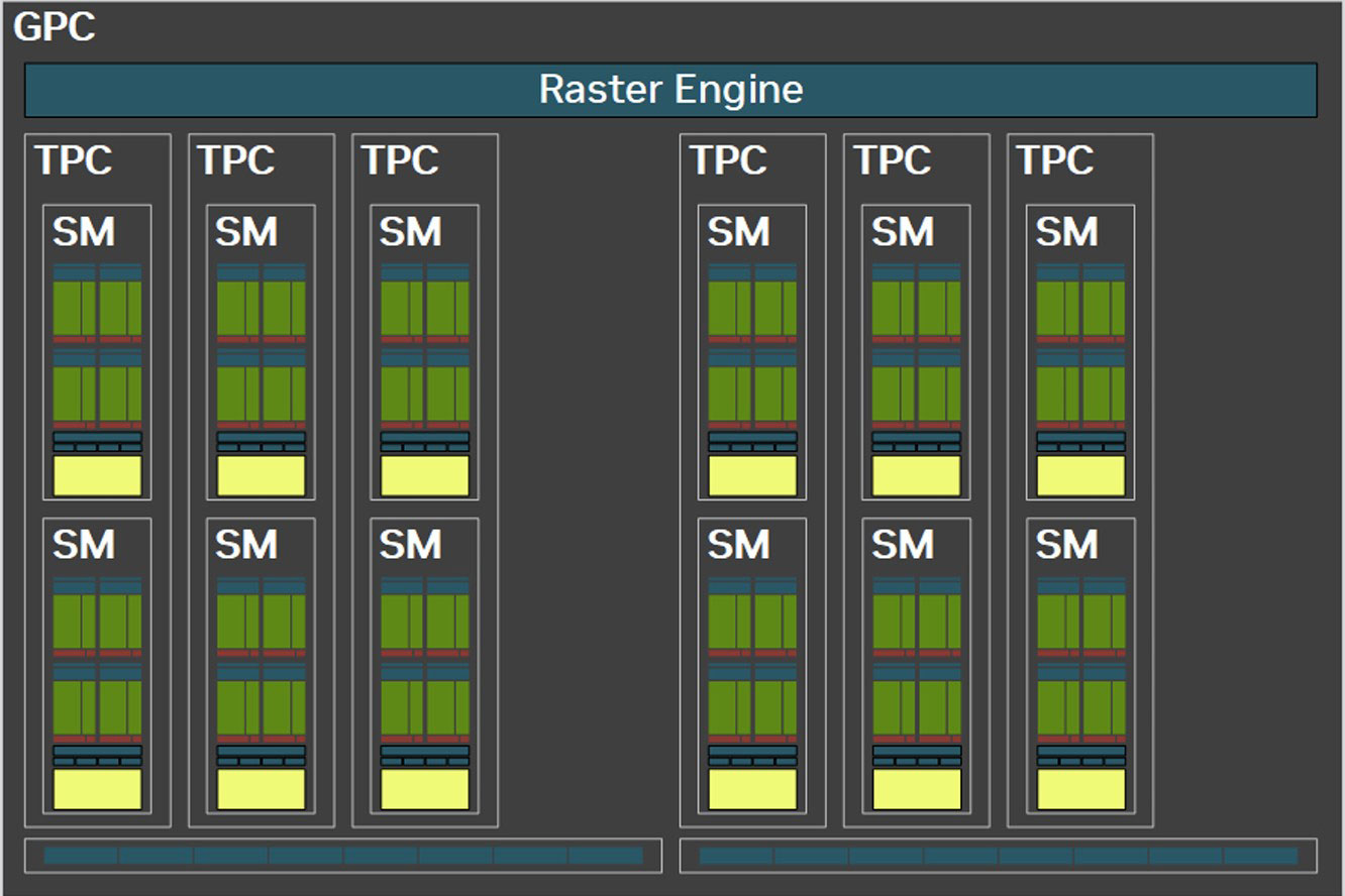
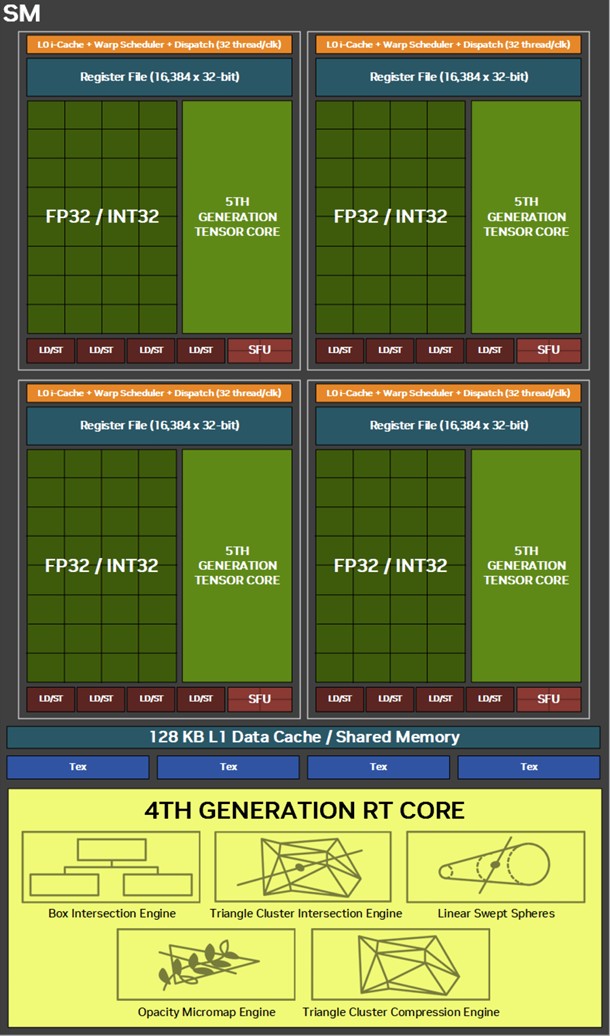
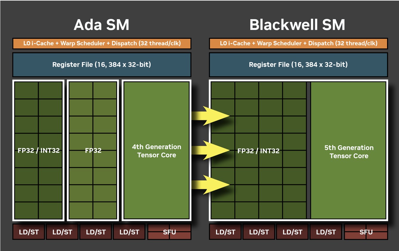
Each graphics processing cluster (GPC) is a subdivision of the GPU with nearly all components needed for graphics rendering. On the GB203, a GPC consists of 12 streaming multiprocessors (SM) across 6 texture processing clusters (TPCs), and a raster engine consisting of 16 ROPs. Each SM contains 128 CUDA cores. Unlike the Ada generation SM that each had 64 FP32+INT32 and 64 purely-FP32 SIMD units, the new Blackwell generation SM features concurrent FP32+INT32 capability on all 128 SIMD units. These 128 CUDA cores are arranged in four slices, each with a register file, a level-0 instruction cache, a warp scheduler, two sets of load-store units, and a special function unit (SFU) handling some special math functions such as trigonometry, exponents, logarithms, reciprocals, and square-root. The four slices share a 128 KB L1 data cache, and four TMUs. The most exotic components of the Blackwell SM are the four 5th Gen Tensor cores, and a 4th Gen RT core.

Perhaps the biggest change to the way the SM handles work introduced with Blackwell is the concept of neural shaders—treating portions of the graphics rendering workload done by a generative AI model as shaders. Microsoft has laid the groundwork for standardization of neural shaders with its Cooperative Vectors API, in the latest update to DirectX 12. The Tensor cores are now accessible for workloads through neural shaders, and the shader execution reordering (SER) engine of the Blackwell SM is able to more accurately reorder workloads for the CUDA cores and the Tensor core in an SM.
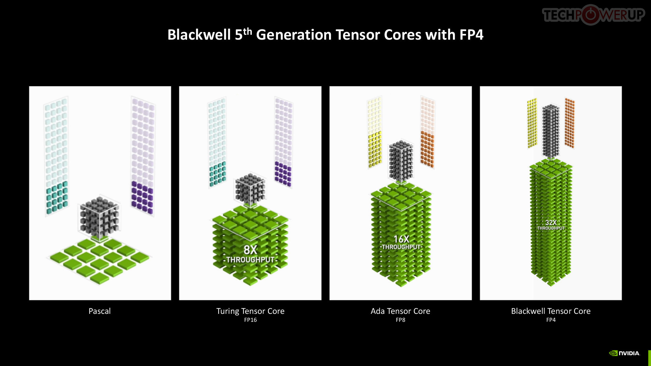
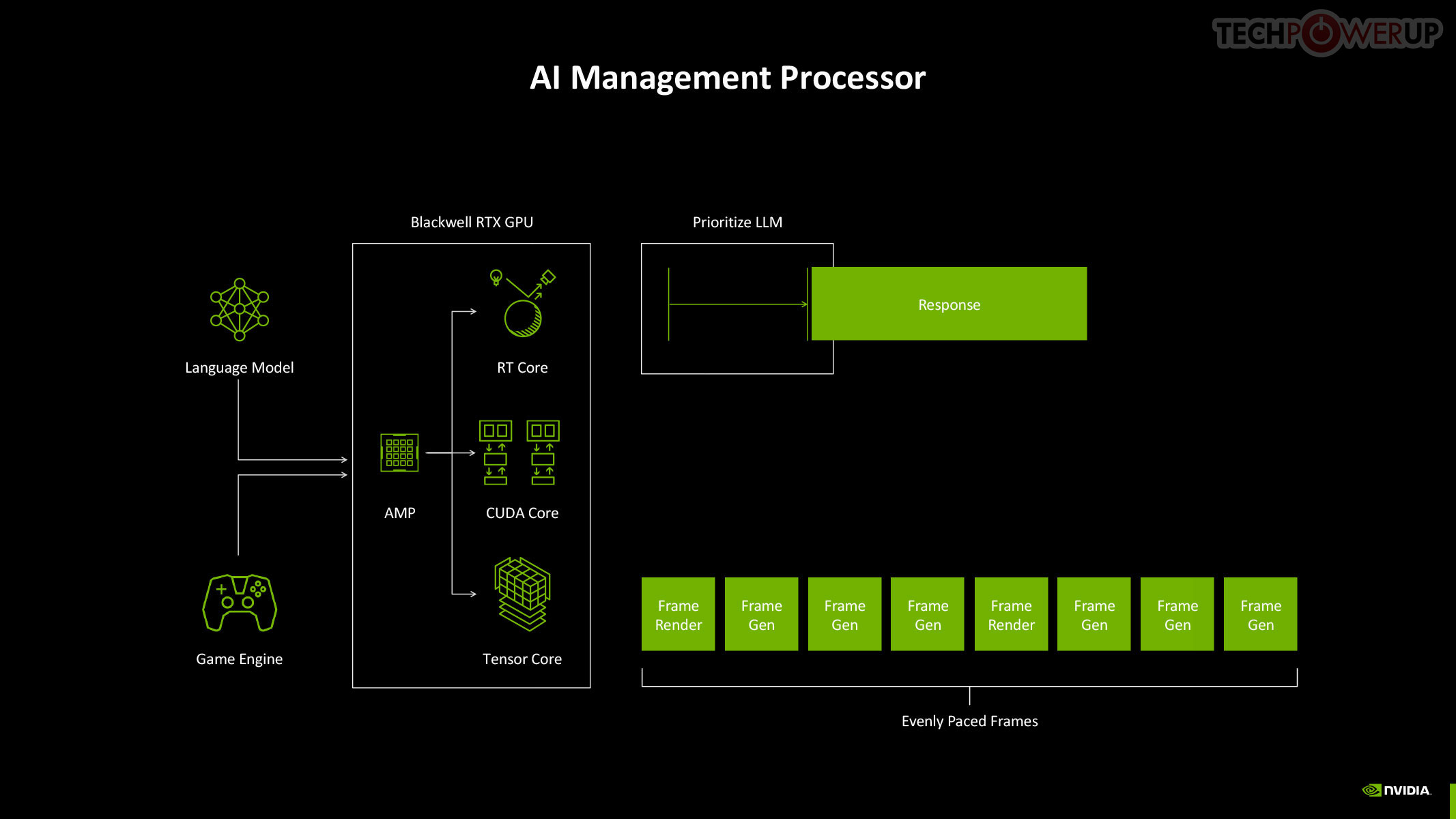
The new 5th Gen Tensor core introduces support for FP4 data format (1/8 precision) to fast moving atomic workloads, providing 32 times the throughput of the very first Tensor core introduced with the Volta architecture. Over the generations, AI models leveraged lesser precision data formats, and sparsity, to improve performance. The AI management processor (AMP) is what enables simultaneous AI and graphics workloads at the highest levels of the GPU, so it could be simultaneously rendering real time graphics for a game, while running an LLM, without either affecting the performance of the other. AMP is a specialized hardware scheduler for all the AI acceleration resources on the silicon. This plays a crucial role for DLSS 4 multi-frame generation to work.
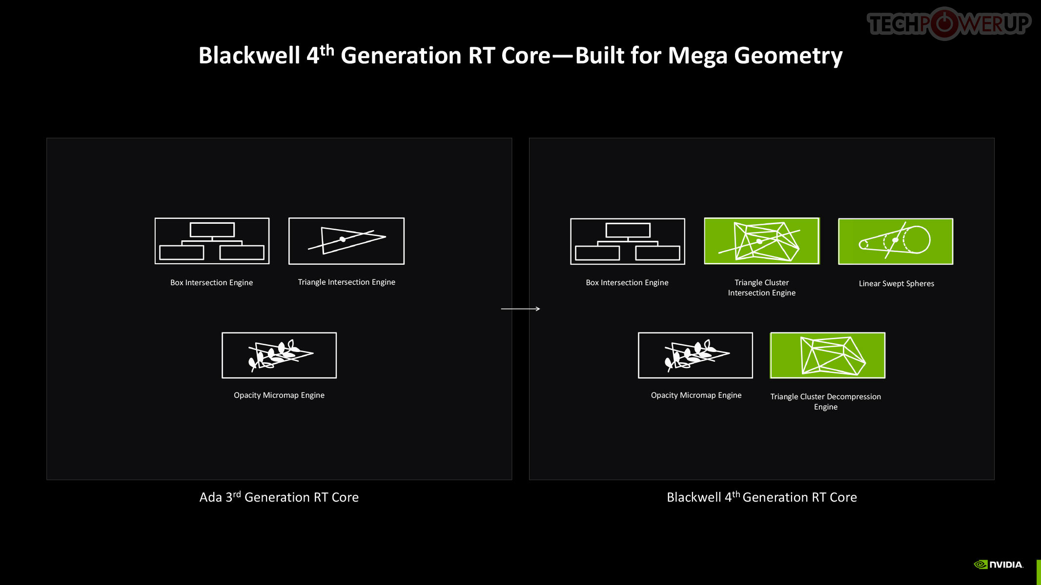
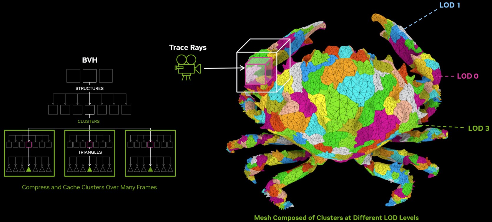
The 4th Gen RT core not just offers a generational increase in ray testing and ray intersection performance, which lowers the performance cost of enabling path tracing and ray traced effects; but also offers a potential generational leap in performance with the introduction of Mega Geometry. This allows for ray traced objects with extremely high polygon counts, increasing their detail. Poly count and ray tracing present linear increases in performance costs, as each triangle has to intersect with a ray, and there should be sufficient rays to intersect with each of them. This is achieved by adopting clusters of triangles in an object as first-class primitives, and cluster-level acceleration structures. The new RT cores introduce a component called a triangle cluster intersection engine, designed specifically for handling mega geometry. The integration of a triangle cluster compression format and a lossless decompression engine allows for more efficient processing of complex geometry.
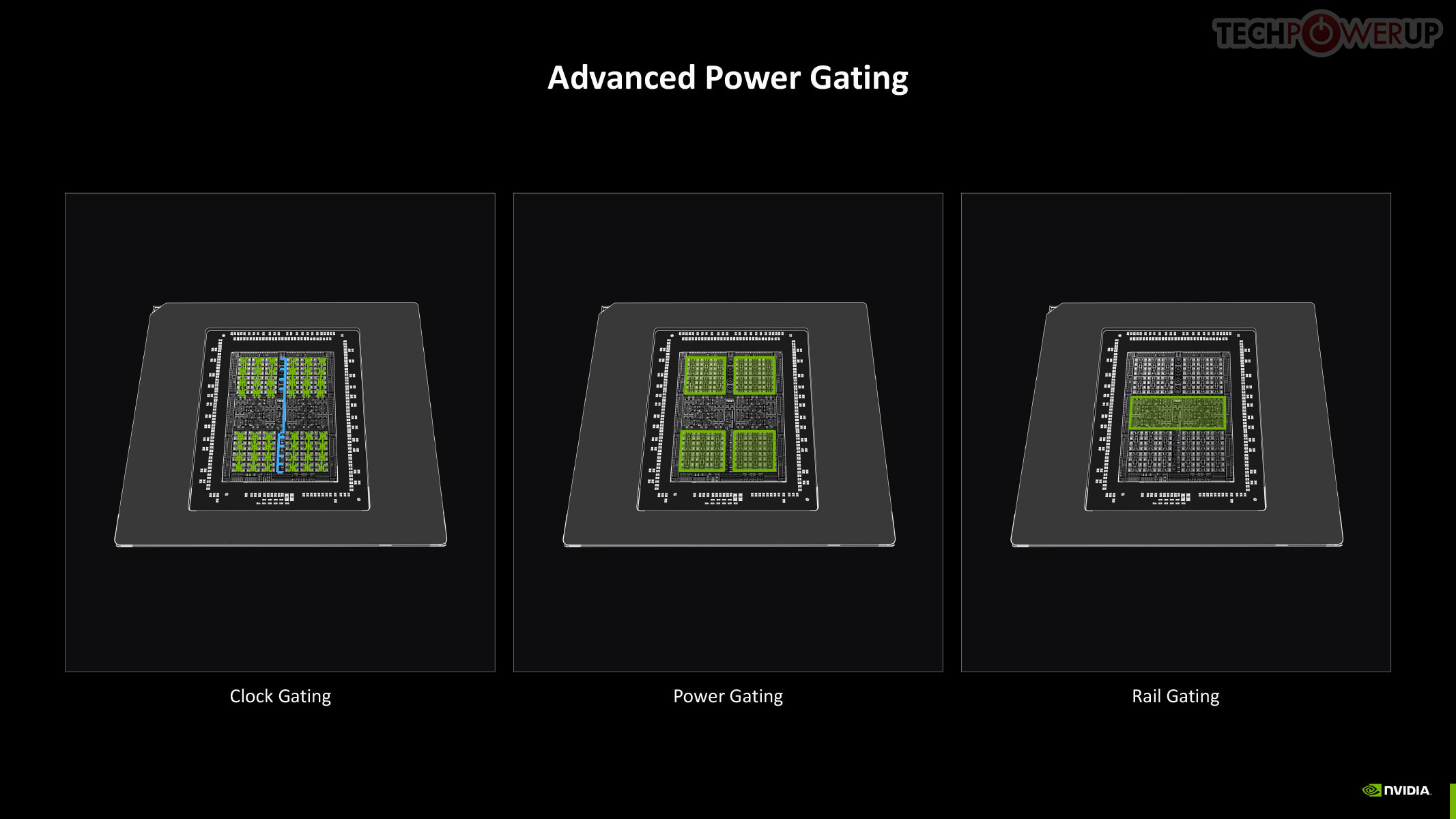
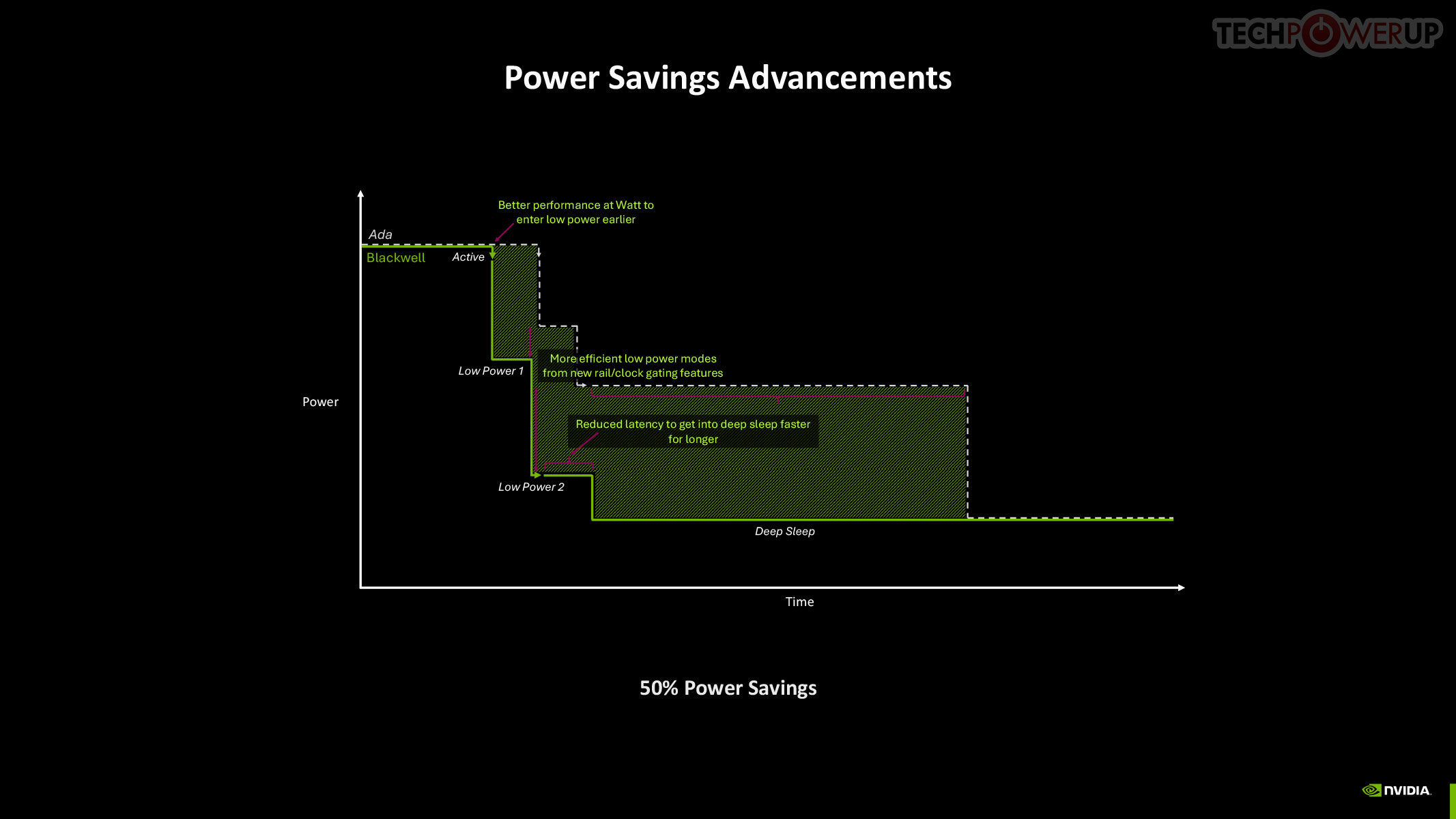
The GB203 and the rest of the GeForce Blackwell GPU family is built on the exact same TSMC "NVIDIA 4N" foundry node, which is actually 5 nm, as previous-generation Ada, so NVIDIA directed efforts to finding innovative new ways to manage power and thermals. This is done through a re-architected power management engine that relies on clock gating, power gating, and rail gating of the individual GPCs and other top-level components. It also worked on the speed at which the GPU makes power-related decisions.
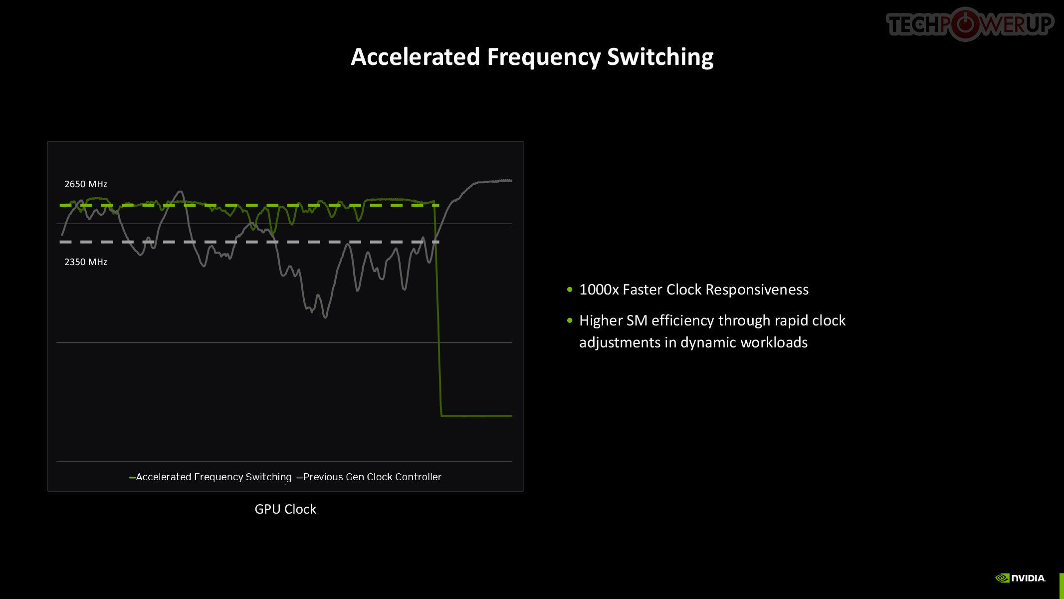
The quickest way to drop power is by adjusting the GPU clock speed, and with Blackwell, NVIDIA introduced a means for rapid clock adjustments at the SM-level.
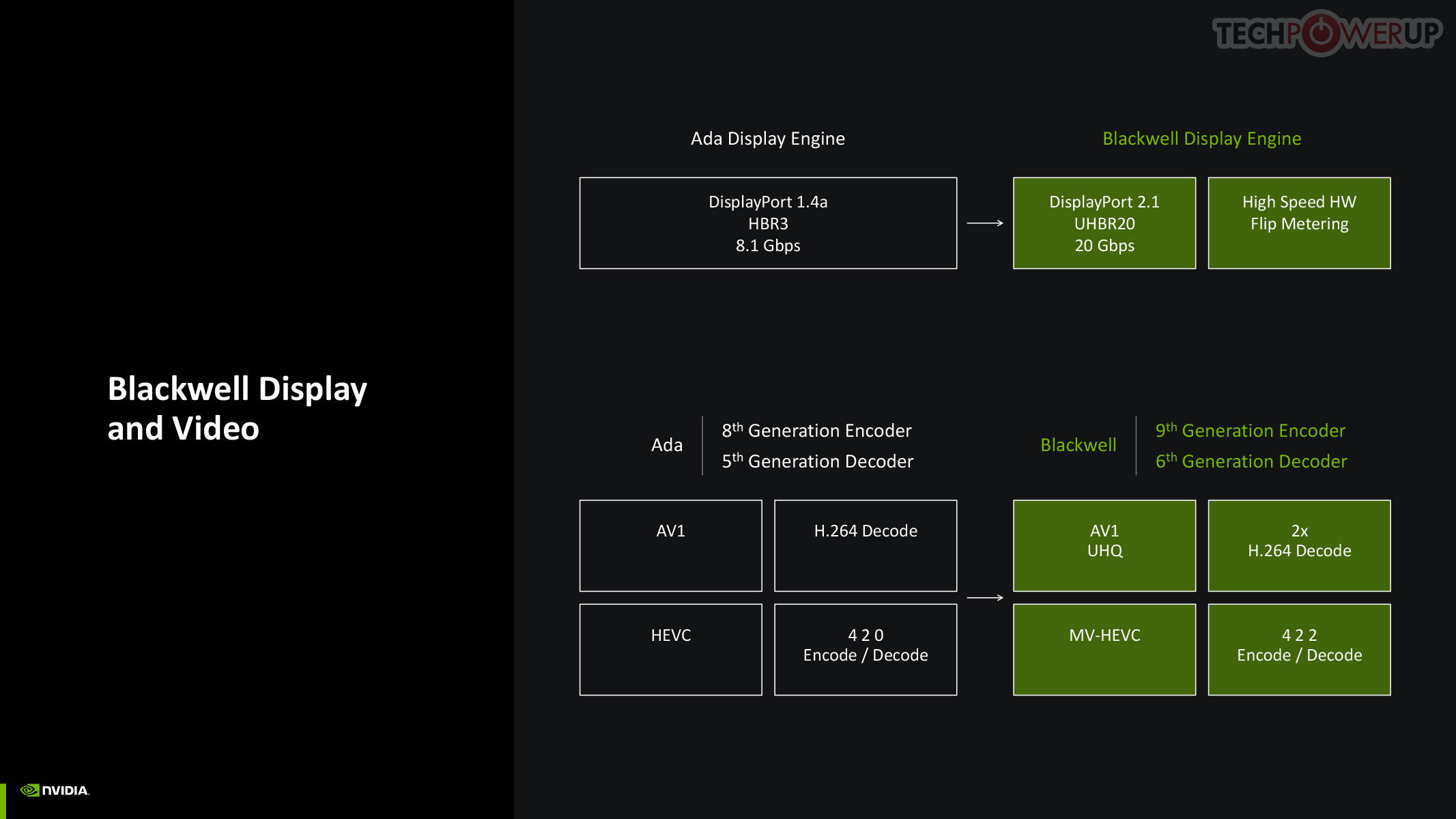
NVIDIA updated both the display engine and the media engine of Blackwell over the previous generation Ada, which drew some flack for holding on to older display I/O standards such as DisplayPort 1.4, while AMD and Intel had moved on to DisplayPort 2.1. The good news is that Blackwell supports DP 2.1 with UHBR20, enabling 8K 60 Hz with a single cable. The company also updated NVDEC and NVENC, which now support AV1 UHQ, double the H.264 decode performance, MV-HEVC, and 4:2:2 formats.
Neural Rendering
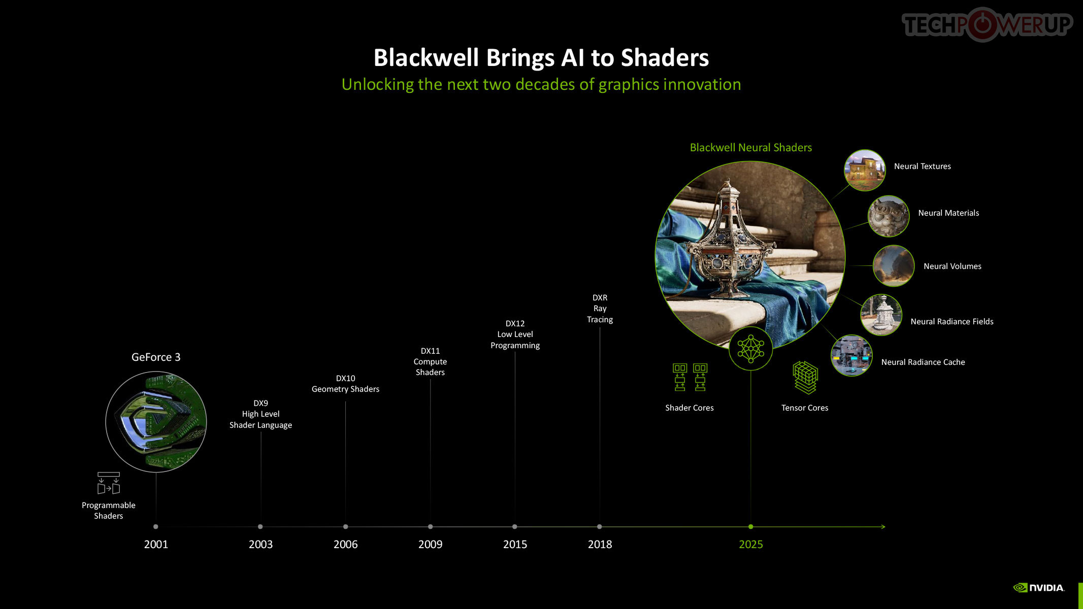
Neural Rendering promises to be as transformative to modern graphics as programmable shaders itself. 3D Graphics rendering evolved from fixed-function over the turn of the century, to programmable shaders, HLSL, geometry shaders, compute shaders, and ray tracing, over the past couple of decades. In 2025, NVIDIA is writing the next chapter in this journey with Blackwell neural shaders. This allows for a host of neural-driven effects, including neural materials, neural volumes, and even neural radiance fields. Microsoft introduced the new Cooperative Vectors API for DirectX in a recent update, making it possible to access Tensor cores within a graphics API. Combined with a new shading language, Slang, this breakthrough enables developers to integrate neural techniques directly into their workflows, potentially replacing parts of the traditional graphics pipeline. Slang splits large, complex functions into smaller pieces that are easier to handle. Given that this is a DirectX standard API feature, there is nothing that stops AMD and Intel from integrating Neural Rendering (Cooperative Vectors) into their graphics drivers.
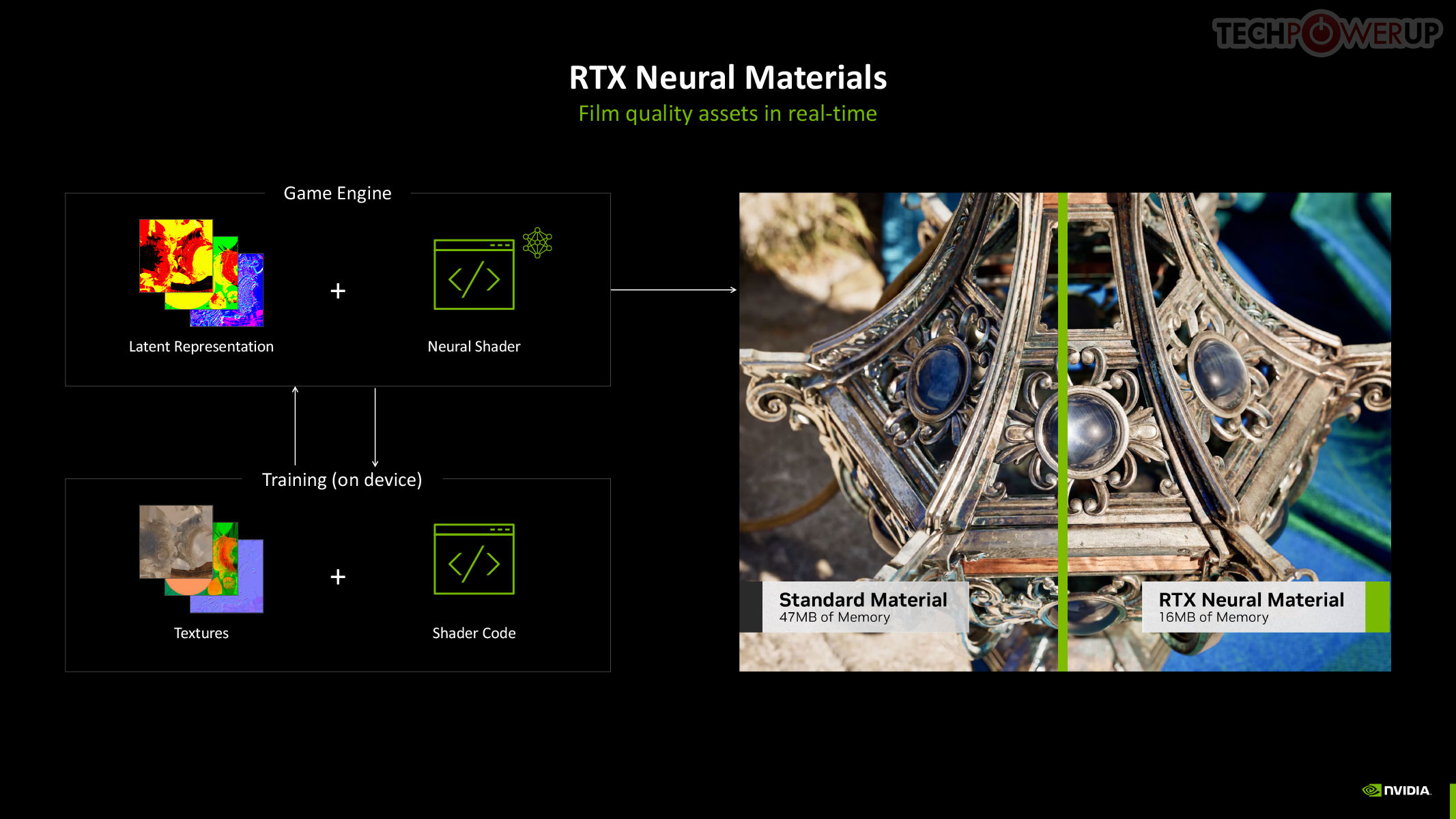
RTX Neural Materials works to significantly reduce the memory footprint of materials in 3D scenes. Under conventional rendering, the memory footprint of a material is bloated from complex shader code. Neural materials convert shader code and texture layers into a compressed neural representation. This results in up to a 7:1 compression ratio and enables small neural networks to generate stunning, film-like materials in real-time. For example, silk rendered with traditional shaders might lack the multicolored sheen seen in real life. Neural materials, however, capture intricate details like color variation and reflections, bringing such surfaces to life with unparalleled realism—and at a fraction of the memory cost.
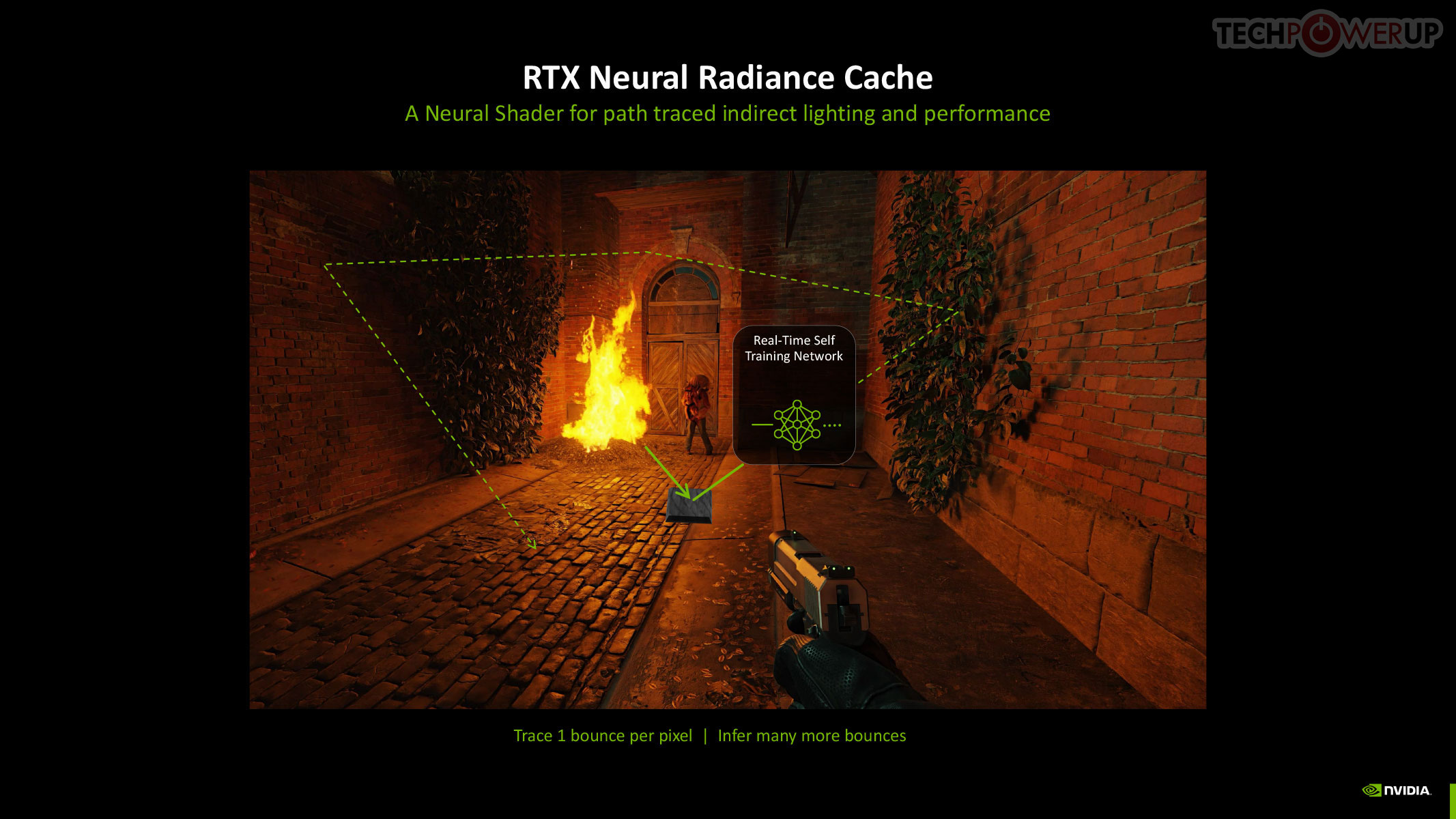
The new Neural Radiance Cache, which dynamically trains a neural network during gameplay using the user's GPU, allowing light transport to be cached spatially, enabling near-infinite light bounces in a scene. This results in realistic indirect lighting and shadows with minimal performance impact. NRC partially traces 1 or 2 rays before storing them in a radiance cache, and infers an infinite amount of rays and bounces for a more accurate representation of indirect lighting in the game scene.
DLSS 4 and Multi Frame Generation
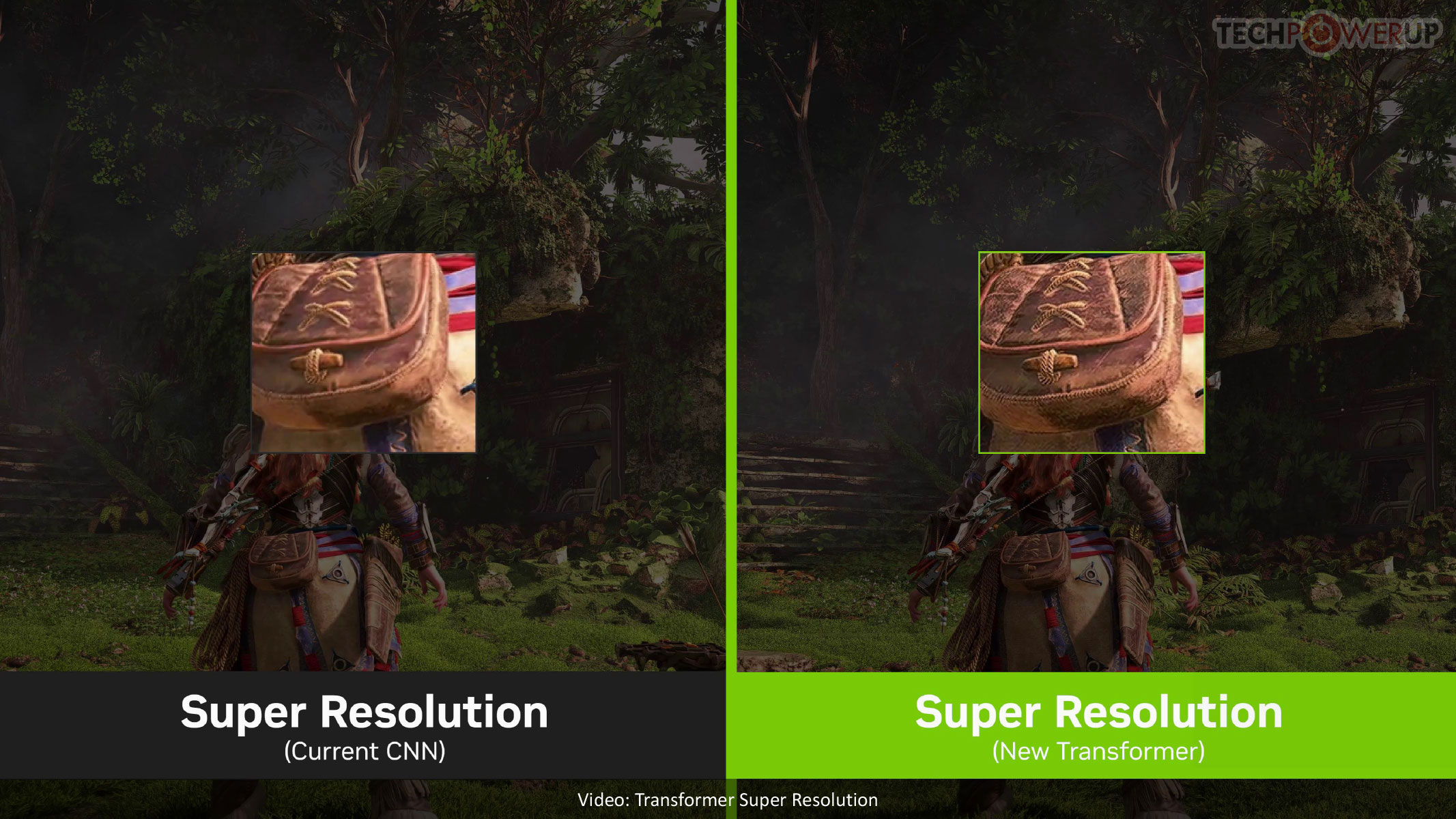
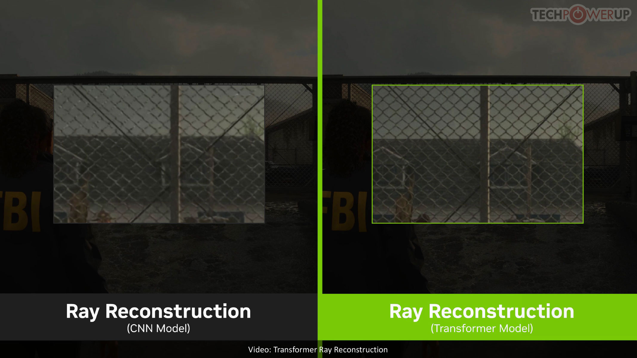
DLSS 4 introduces a major leap in image quality and performance. It isn't just a version bump with the introduction of a new feature, namely Multi Frame Generation, but introduces updates to nearly all DLSS sub-features. DLSS from its very beginning relied on AI to reconstruct details in super resolution, and with DLSS 4, NVIDIA is introducing a new transformer-based AI model to succeed the convolutional neural networks previous used, for double the parameters, four times the compute performance, and significantly improved image quality. Ray Reconstruction, introduced with DLSS 3.5, gets a significant image quality update with the new transformer-based model.
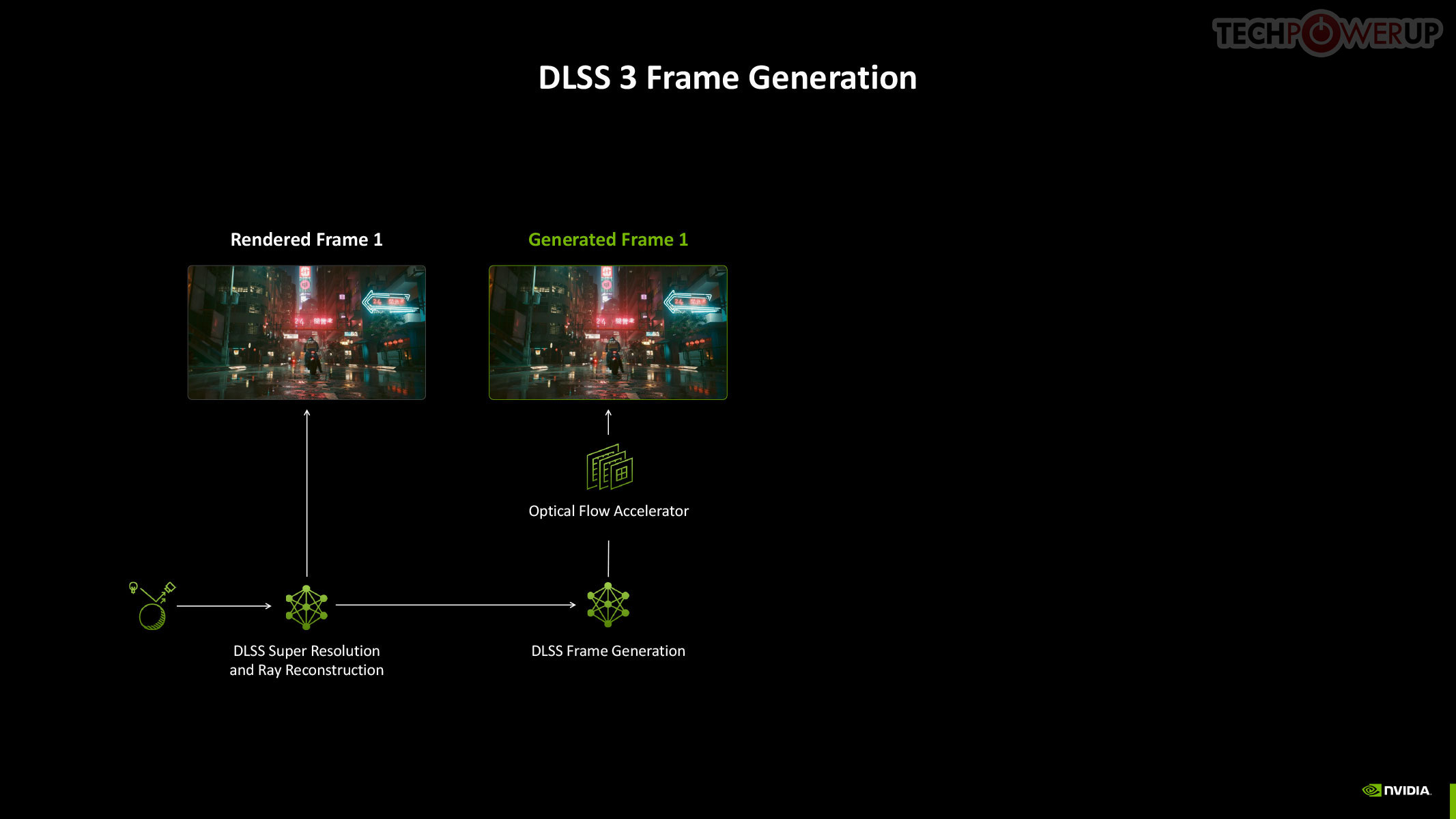
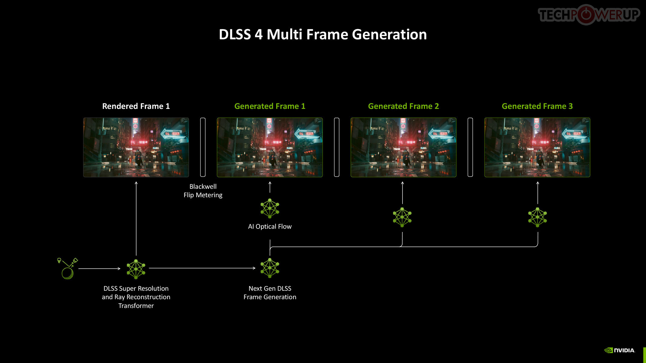
To understand Multi Frame Generation, you need to understand how DLSS Frame Generation, introduced with GeForce Ada, works. An Optical Flow Accelerator component gives the DLSS algorithm data to generate an entire frame using a neural network, using information from a previous rendered frame, effectively doubling frame rate. In Multi Frame Generation, AI takes over the functions of optical flow, to predict up to three frames following a conventionally rendered frame, effectively drawing four frames form the rendering effort of one.
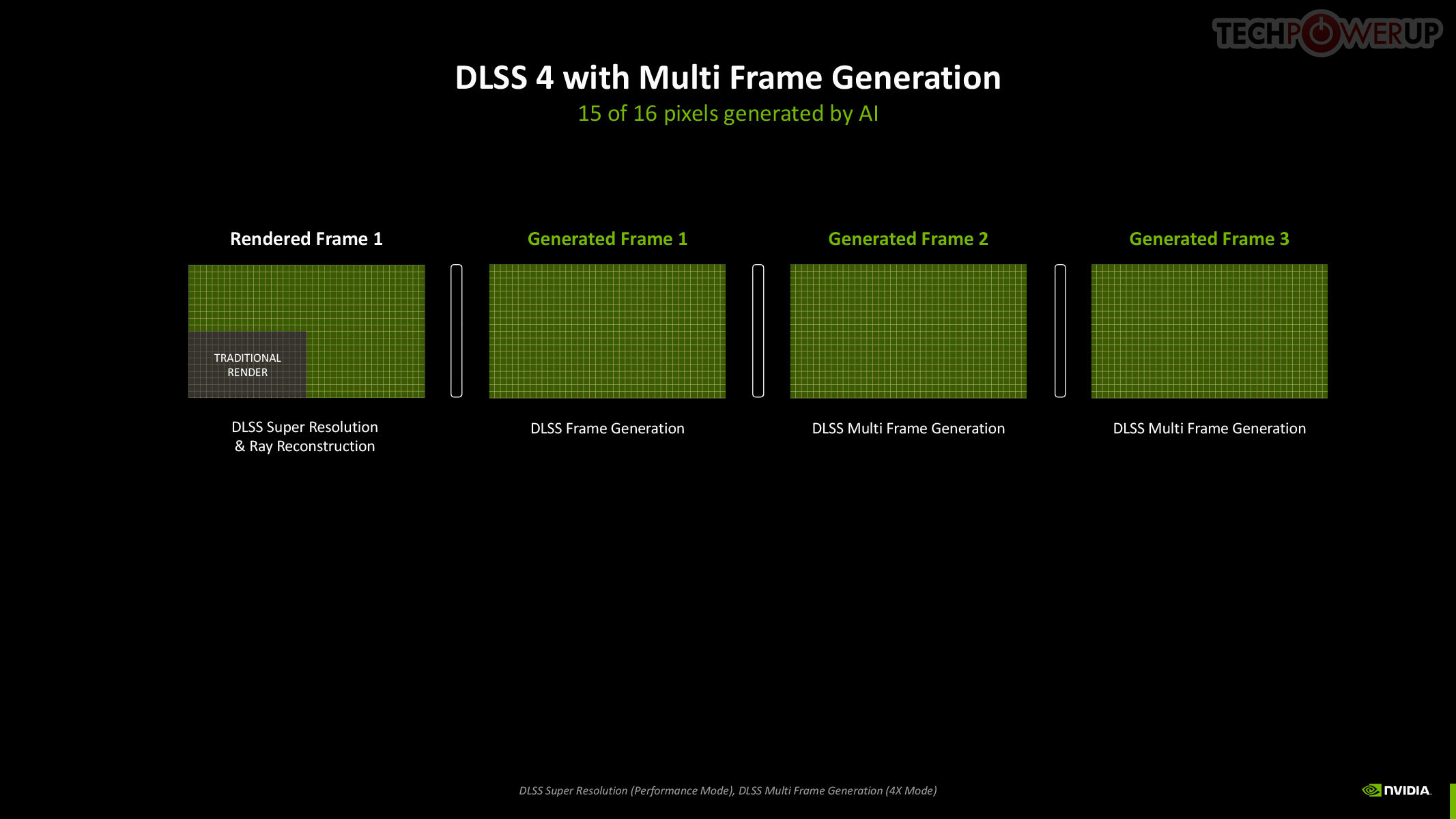
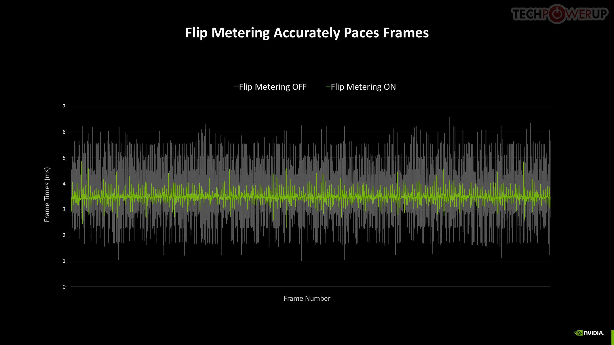
Now, assuming this rendered frame is a product of Super Resolution, with the maximum performance setting generating 4x the pixels from a single rendered pixel, you're looking at a possibility where the rendering effort of 1/4th a frame goes into drawing 4 frames, or 15 in every 16 pixels being generated entirely by DLSS. When generating so many frames, Frame Pacing becomes a problem—irregular frame intervals impact smoothness. DLSS 4 addresses these issues by using a dedicated hardware unit inside Blackwell, which takes care of flip metering, reducing frame display variability by 5-10x. The Display Engine of Blackwell contains the hardware for flip metering.
NVIDIA Reflex 2
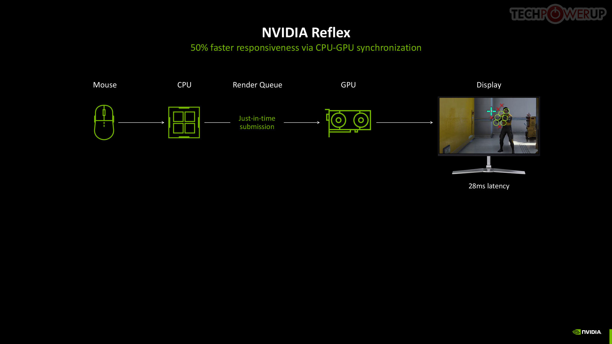
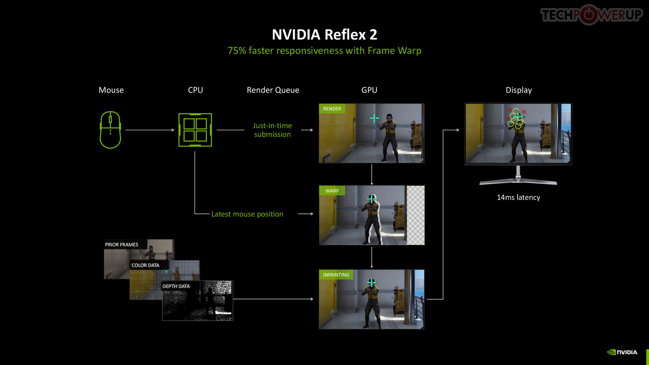
The original NVIDIA Reflex brought about a significant improvement to the responsiveness of maxed out graphics in competitive online gameplay, by compacting the rendering queue with the goal of reducing the whole system latency by up to 50%. Reflex is mandatory in DLSS 3 Frame Generation, given the latency cost imposed by the technology. Multi-frame generation calls for an equally savvy piece of technology, so we hence have Reflex 2. NVIDIA claims to have achieved a 75% reduction in latency with Frame Warp, which updates the camera (viewport) positions based on user inputs in real-time, and then uses temporal information to reconstruct the frame to display.
Packaging
The Card
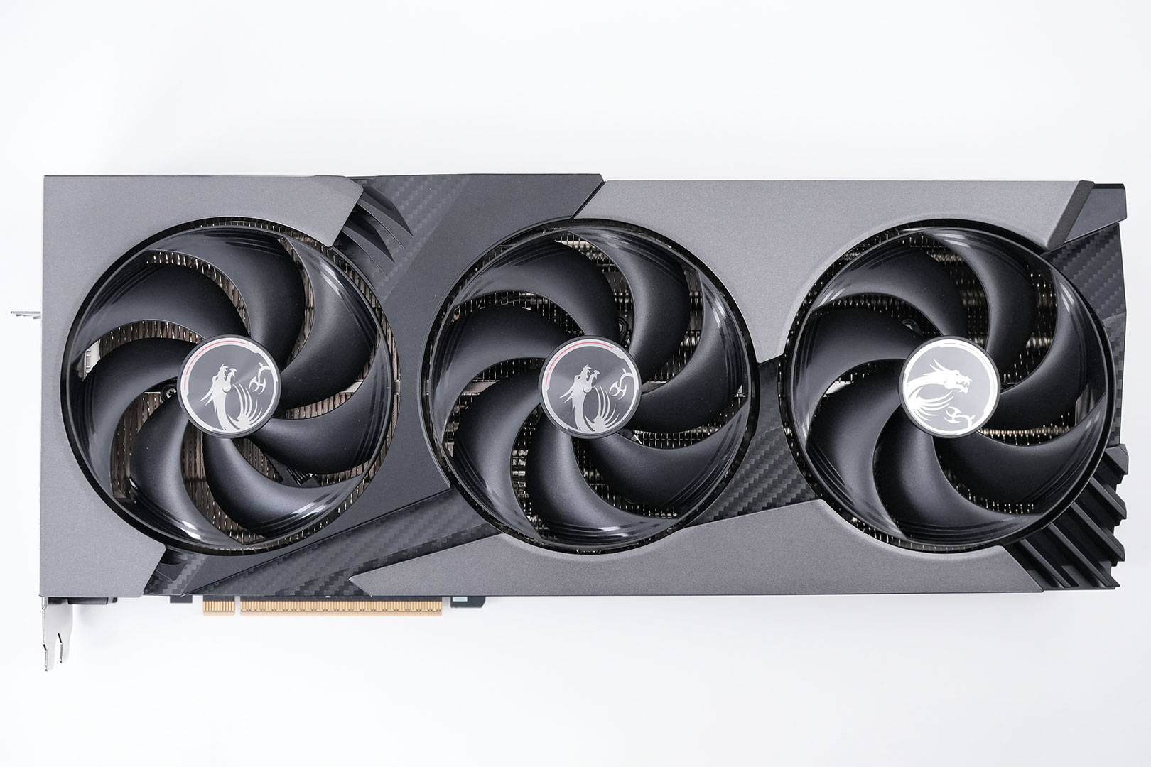
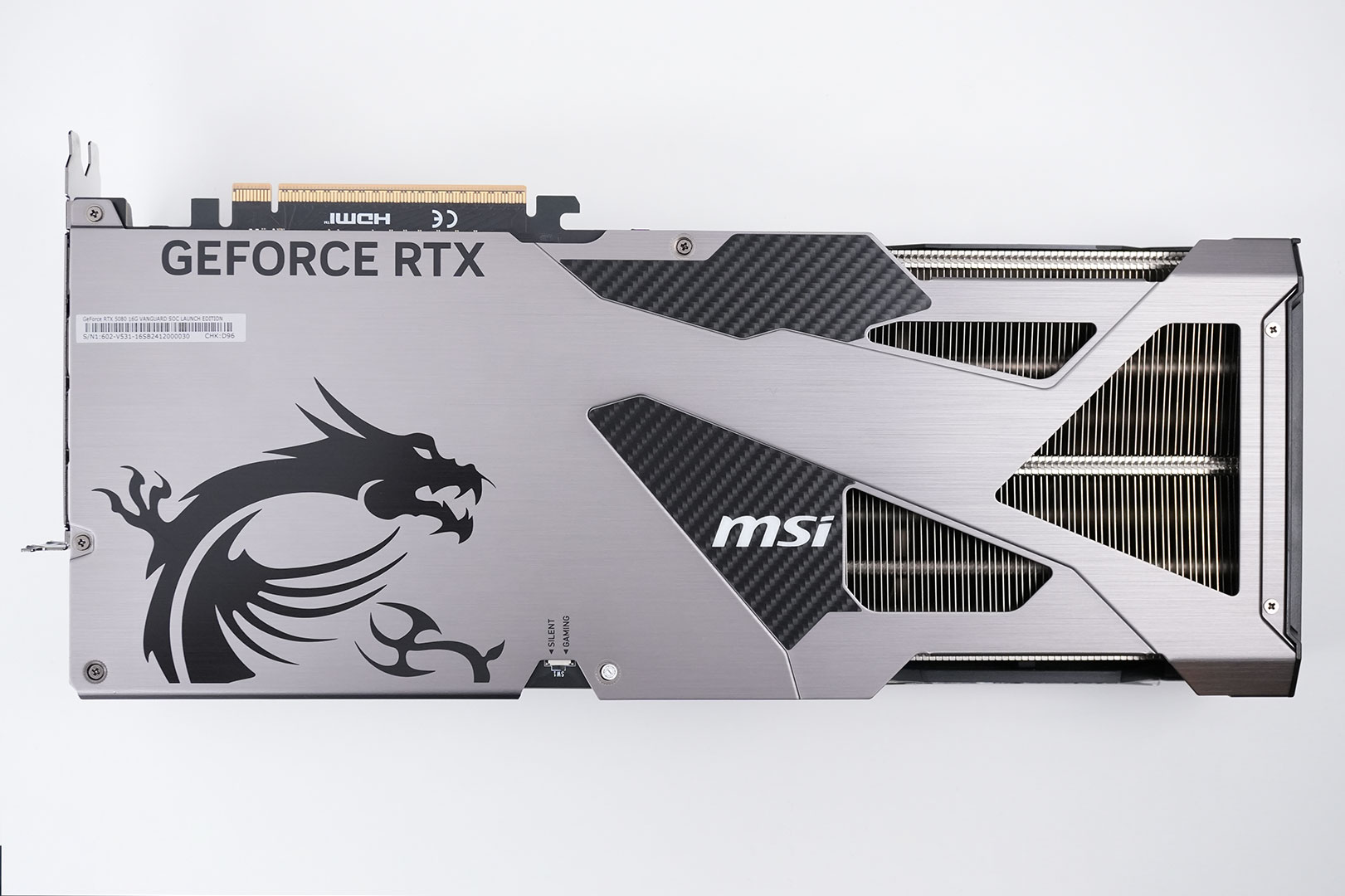
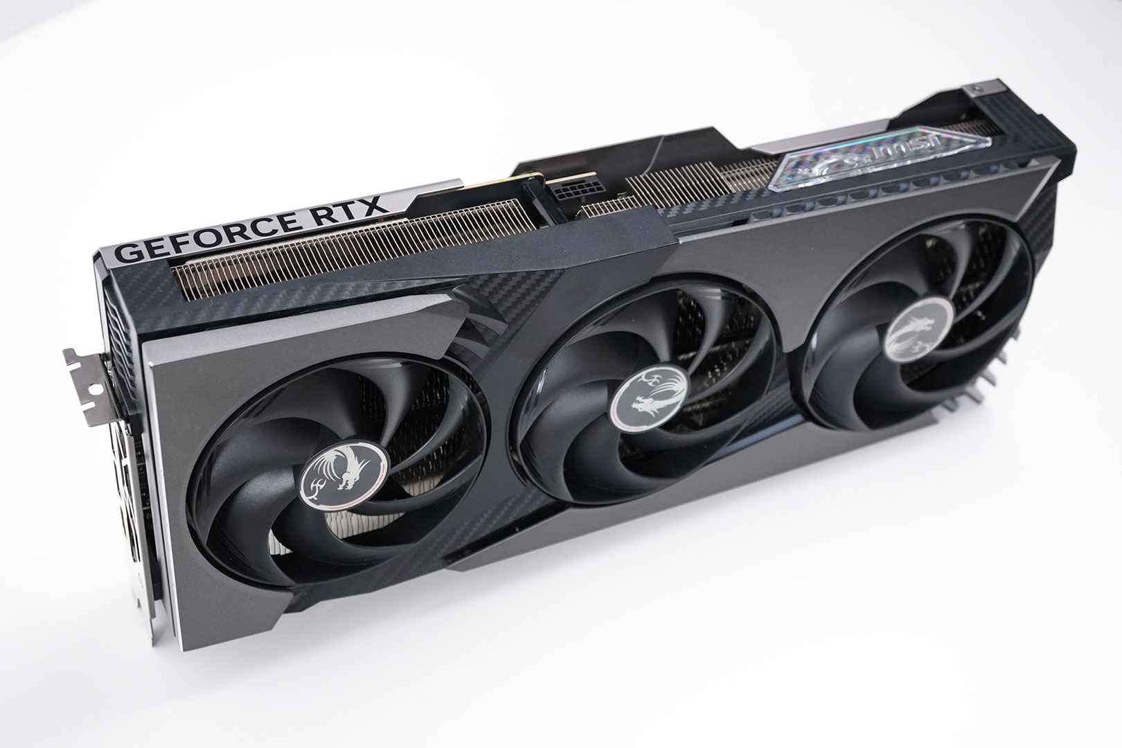
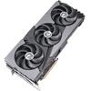
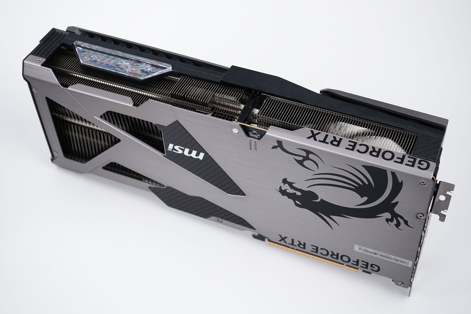
Vanguard is MSI's new GPU lineup and the cards are looking good. The color theme is still metal, with highlights in various shades of gray, but the color theme is a bit darker than Suprim—I like. On the back you get a metal backplate with a large cutout.
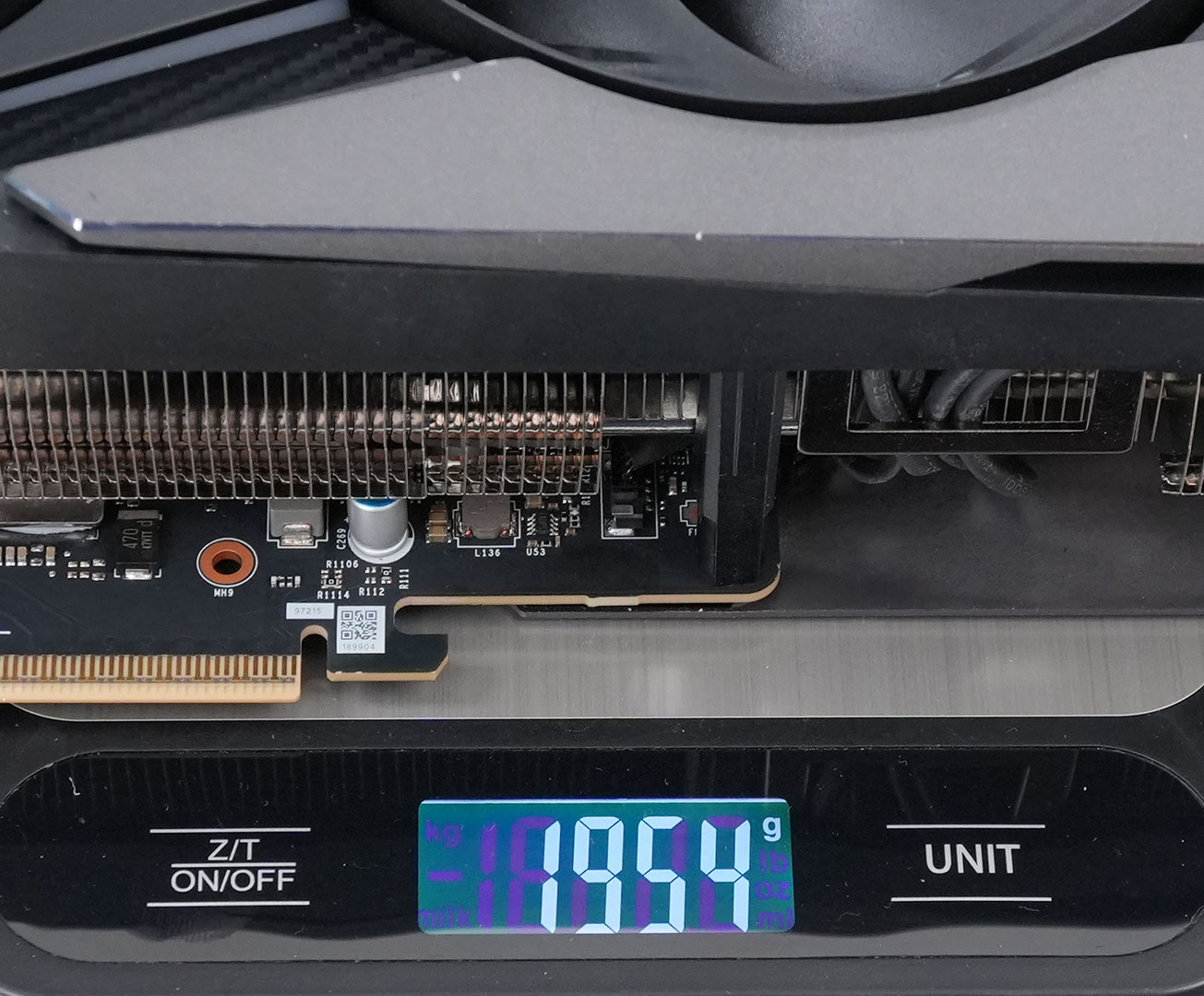
Dimensions of the card are 36.0 x 15.0 cm, and it weighs 1954 g.
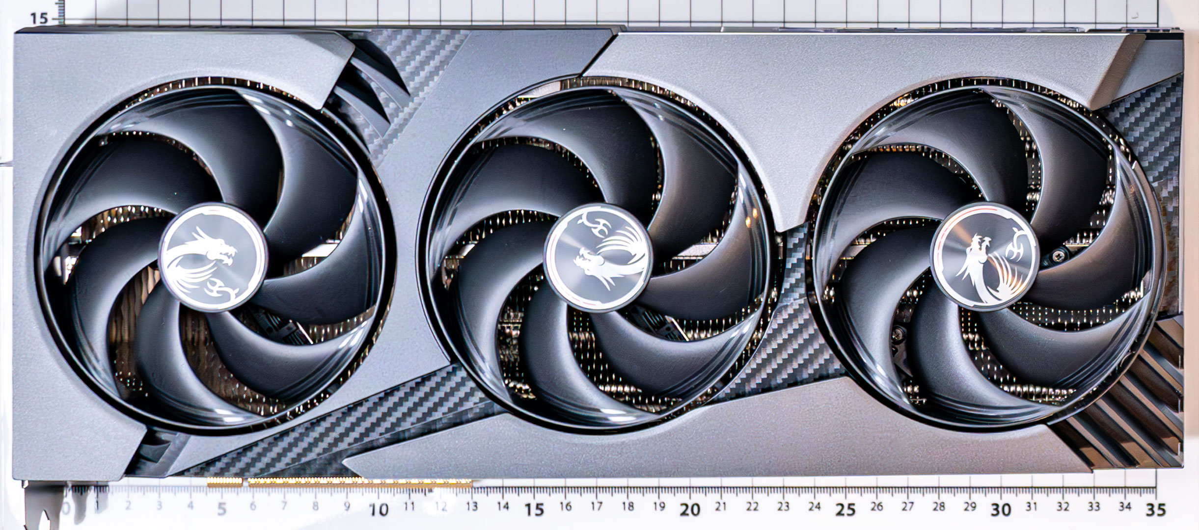
Installation requires three slots in your system. We measured the card's width to be 67 mm.
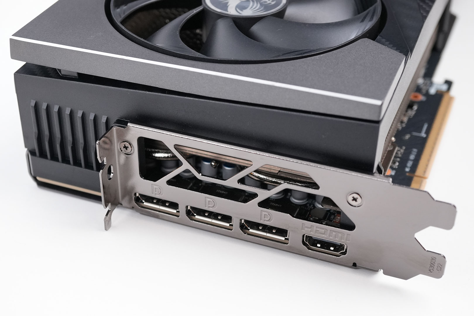
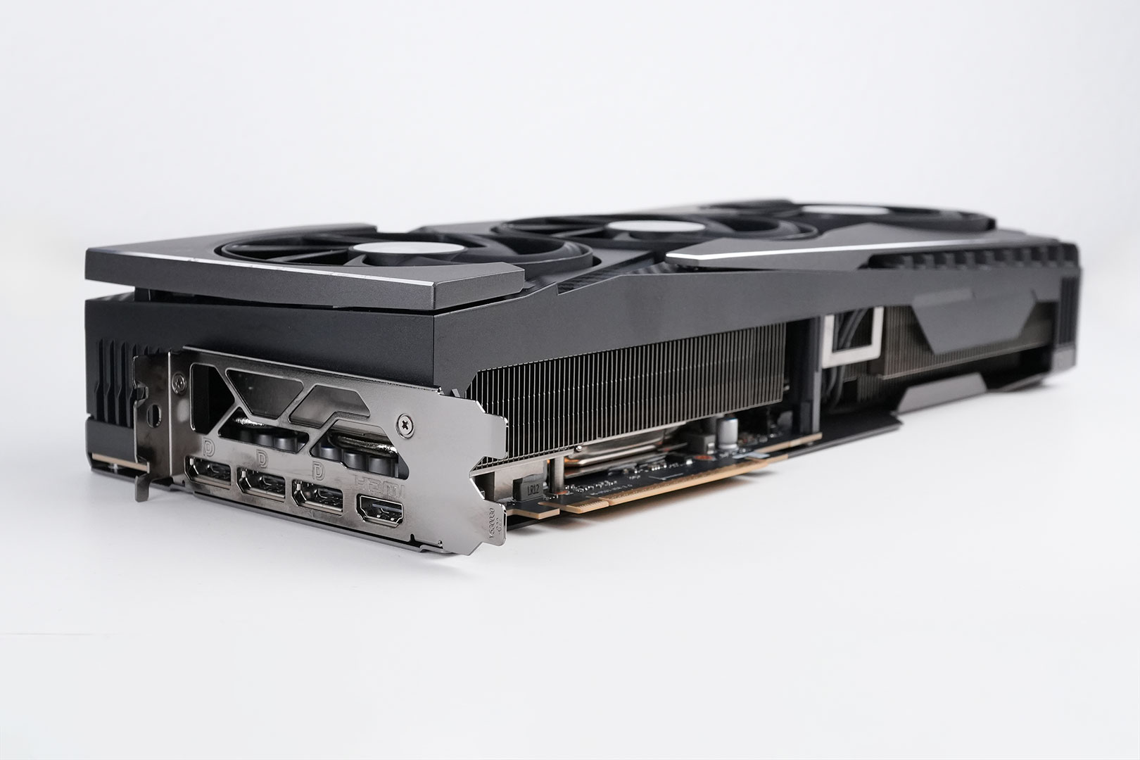
Display connectivity includes three standard DisplayPort 2.1b and one HDMI 2.1b.
Standard for all GeForce RTX 50-series Blackwell cards is a new display engine that supports three DisplayPort 2.1b outputs, each capable of UHBR20; and one HDMI 2.1a. Both interfaces support DSC (display stream compression). With DSC enabled, a single DisplayPort on this card can drive 4K 12-bit HDR at 480 Hz; or 8K 12-bit HDR at up to 165 Hz. The RTX 5080 features an updated media acceleration engine with support for 4:2:2 video formats, AV1 UHQ, and MV-HEVC. There are two independent NVENC and NVDEC units.
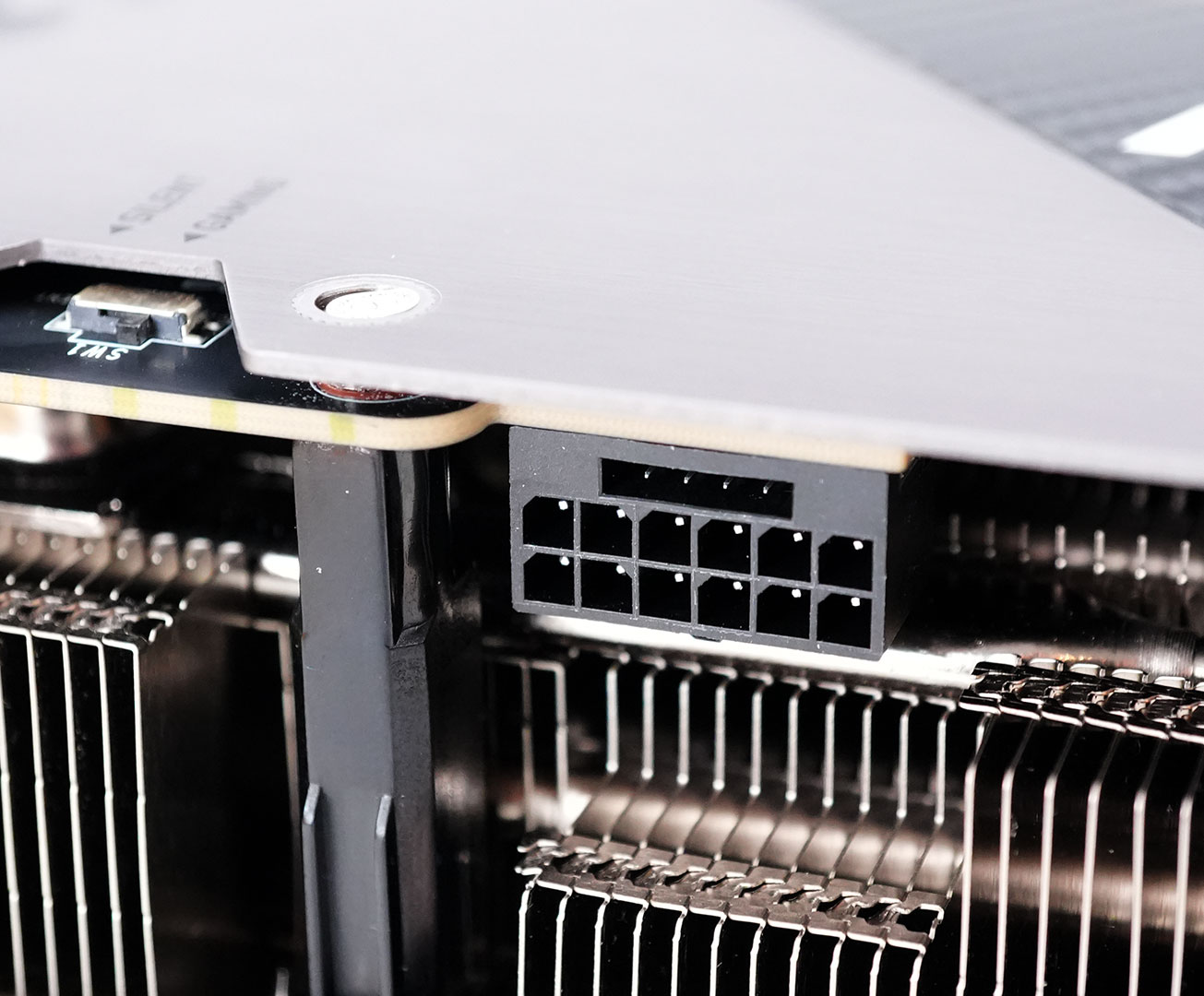
The card uses a single 16-pin connector, which allows a maximum power draw of 600 W.
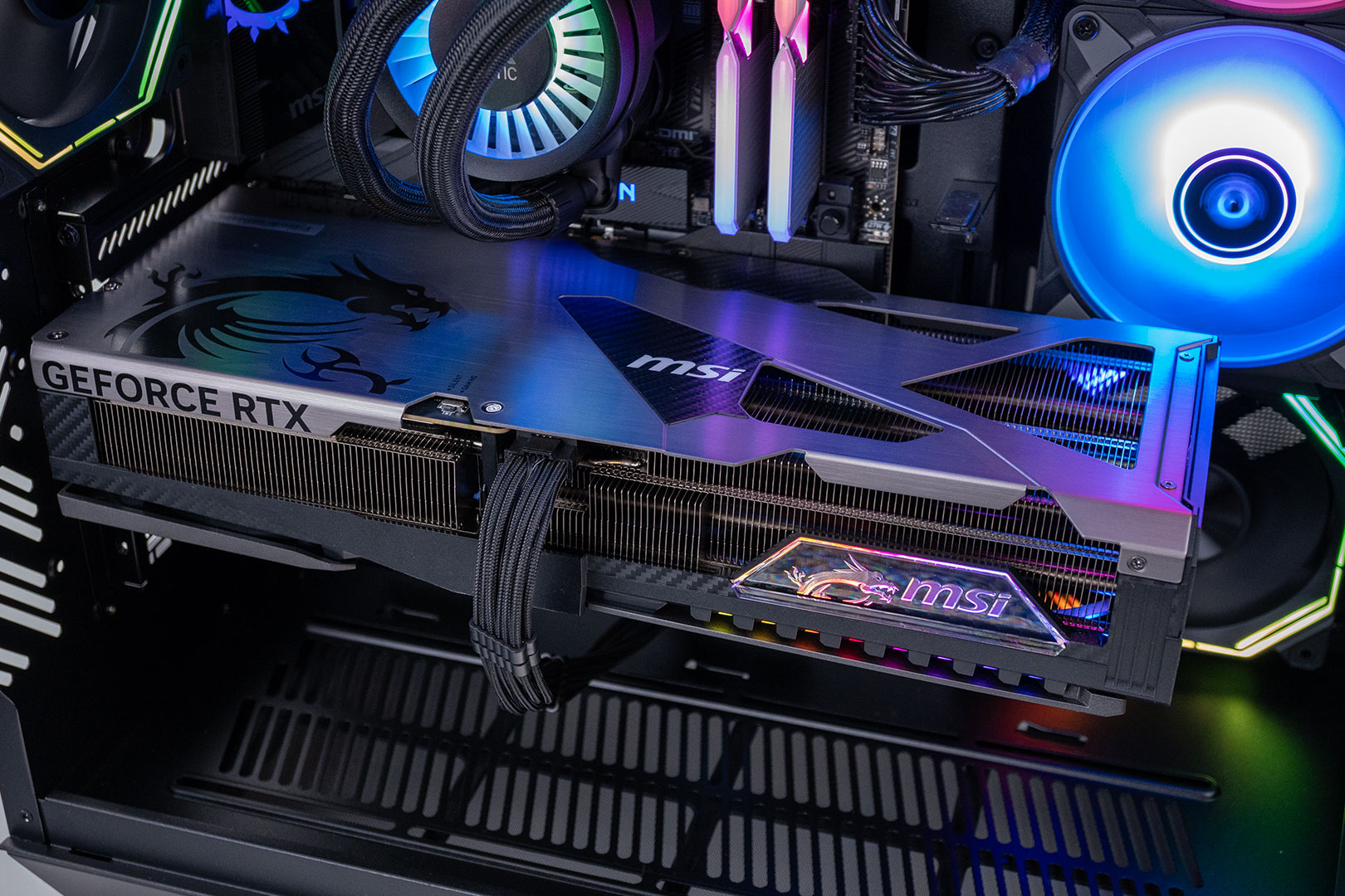
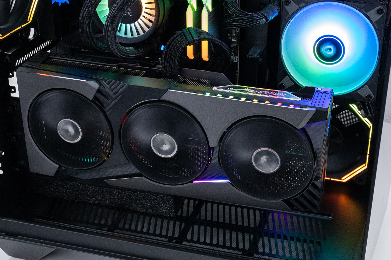
MSI has added an RGB illumination zone on the MSI logo and a lighting strip near the fans.
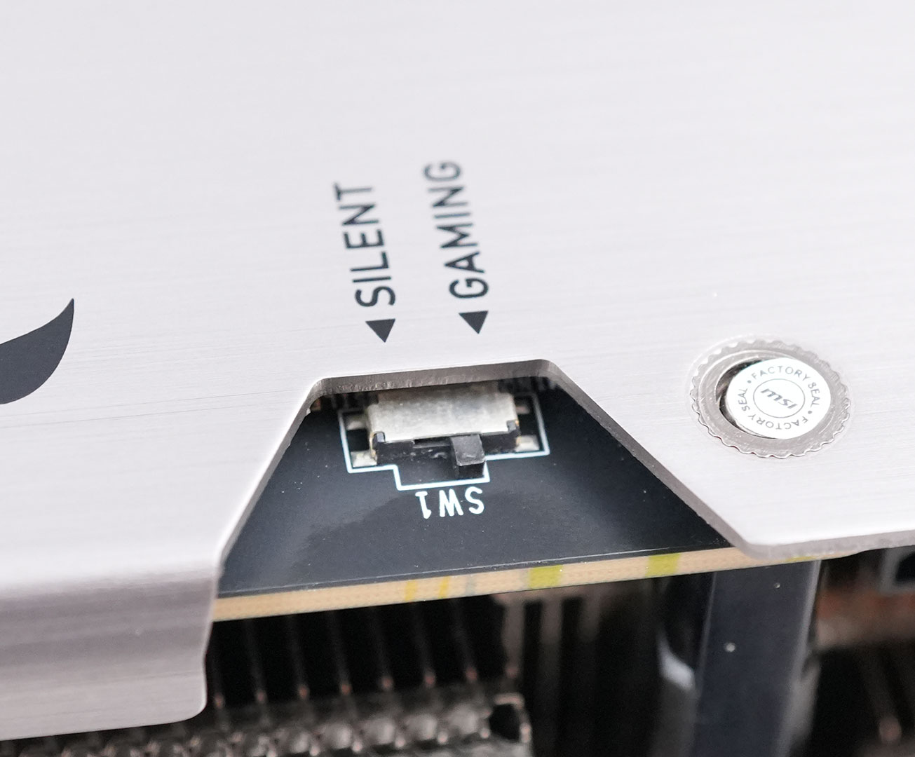
The dual BIOS switch lets you switch from the default "Performance" BIOS to a "Quiet" BIOS that runs a more relaxed fan curve.
Our Patreon Silver Supporters can read articles in single-page format.
May 4th, 2025 08:27 EDT
change timezone
Latest GPU Drivers
New Forum Posts
- Milestones (14020)
- WCG Daily Numbers (12858)
- Post Your CyberPunk 2077 Benchmark (2024 edition) (124)
- Old NVIDIA GPU with torn branding sticker - what’s the brand? (5)
- TPU's Rosetta Milestones and Daily Pie Thread (2299)
- Ssd failure, I don’t know what to do (27)
- Free Games Thread (4658)
- Are the 8 GB cards worth it? (815)
- Technical Issues - TPU Main Site & Forum (2025) (167)
- TPU's WCG/BOINC Team (34499)
Popular Reviews
- Clair Obscur: Expedition 33 Performance Benchmark Review - 33 GPUs Tested
- ASUS ROG Maximus Z890 Hero Review
- ASUS Radeon RX 9070 XT TUF OC Review
- Montech HS02 PRO Review
- NVIDIA GeForce RTX 5060 Ti 8 GB Review - So Many Compromises
- ASUS GeForce RTX 5090 Astral Liquid OC Review - The Most Expensive GPU I've Ever Tested
- Seasonic Vertex GX 850 W Review
- Upcoming Hardware Launches 2025 (Updated Apr 2025)
- ASRock Radeon RX 9070 XT Taichi OC Review - Excellent Cooling
- Team Group GC Pro 2 TB Review
Controversial News Posts
- NVIDIA GeForce RTX 5060 Ti 16 GB SKU Likely Launching at $499, According to Supply Chain Leak (182)
- AMD Radeon RX 9060 XT to Roll Out 8 GB GDDR6 Edition, Despite Rumors (129)
- NVIDIA Sends MSRP Numbers to Partners: GeForce RTX 5060 Ti 8 GB at $379, RTX 5060 Ti 16 GB at $429 (128)
- NVIDIA Launches GeForce RTX 5060 Series, Beginning with RTX 5060 Ti This Week (115)
- Nintendo Confirms That Switch 2 Joy-Cons Will Not Utilize Hall Effect Stick Technology (105)
- NVIDIA PhysX and Flow Made Fully Open-Source (95)
- Sony Increases the PS5 Pricing in EMEA and ANZ by Around 25 Percent (84)
- Parts of NVIDIA GeForce RTX 50 Series GPU PCB Reach Over 100°C: Report (78)