 37
37
MSI GTX 750 Ti Gaming 2 GB Review
(37 Comments) »Introduction
Here it is, NVIDIA's GeForce GTX 750 Ti, one of the first GPUs based on its next-generation "Maxwell" GPU architecture. First reports of the chip being based on "Maxwell" hit us by surprise as we presumed that a new micro-architecture is invariably pegged to NVIDIA's foundry partner, TSMC, to launch its next-generation 20 nanometer silicon fabrication process. The fact that TSMC's 20 nm node isn't in a position to ship out such complex ASICs as graphics processors right now and that NVIDIA wouldn't want its new architecture to in any way be hit by unforeseen issues arising out of the move to a new process may have led to the decision to use the existing 28 nanometer process.
The GeForce GTX 750 Ti and the GTX 750 (also launched today) are based on the 28 nm GM107 (GeForce-Maxwell 107) silicon. This 1.87 billion-transistor GPU features a basic component hierarchy that's not too different from that of "Kepler," but sees some under-the-hood changes in the design of its key parallel processing sub-unit, the streaming multiprocessor "Maxwell" (SMM). The GTX 750 Ti is positioned between the GTX 760 and GTX 660, which is a sizable gap to fill. NVIDIA is promising some huge performance-per-watt gains with "Maxwell." Given that the GM107 is based on the same 28 nm process as the GeForce Kepler series, there's only one way NVIDIA can deliver on its promise - by developing a better overall architecture.

MSI's GeForce GTX 750 Ti Gaming comes with the company's mighty TwinFrozr dual-fan cooler, which provides plenty of cooling performance for the GTX 750 Ti GPU. The card is also overclocked to 1085 MHz out of the box, which should provide a quick and easy performance boost.
MSI states that their GTX 750 Ti Gaming will retail at $200, which is a hefty $50 (or 33%) price increase.
| GeForce GTX 650 Ti | Radeon HD 7790 | Radeon HD 7850 | GeForce GTX 750 | Radeon R7 260X | GTX 650 Ti Boost | GeForce GTX 750 Ti | MSI GTX 750 Ti Gaming | Radeon R7 265 | GeForce GTX 660 | Radeon HD 7870 | Radeon R9 270X | GeForce GTX 660 Ti | GeForce GTX 760 | |
|---|---|---|---|---|---|---|---|---|---|---|---|---|---|---|
| Shader Units | 768 | 896 | 1024 | 512 | 896 | 768 | 640 | 640 | 1024 | 960 | 1280 | 1280 | 1344 | 1152 |
| ROPs | 16 | 16 | 32 | 16 | 16 | 24 | 16 | 16 | 32 | 24 | 32 | 32 | 24 | 32 |
| Graphics Processor | GK106 | Bonaire | Pitcairn | GM107 | Bonaire | GK106 | GM107 | GM107 | Pitcairn | GK106 | Pitcairn | Pitcairn | GK104 | GK104 |
| Transistors | 2540M | 2080M | 2800M | 1870M | 2080M | 2540M | 1870M | 1870M | 2800M | 2540M | 2800M | 2800M | 3500M | 3500M |
| Memory Size | 1024 MB | 1024 MB | 2048 MB | 1024 MB | 2048 MB | 2048 MB | 2048 MB | 2048 MB | 2048 MB | 2048 MB | 2048 MB | 2048 MB | 2048 MB | 2048 MB |
| Memory Bus Width | 128 bit | 128 bit | 256 bit | 128 bit | 128 bit | 192 bit | 128 bit | 128 bit | 256 bit | 192 bit | 256 bit | 256 bit | 192 bit | 256 bit |
| Core Clock | 925 MHz | 1000 MHz | 860 MHz | 1020 MHz+ | 1100 MHz | 980 MHz+ | 1020 MHz+ | 1085 MHz+ | 925 MHz | 980 MHz+ | 1000 MHz | 1050 MHz | 915 MHz+ | 980 MHz+ |
| Memory Clock | 1350 MHz | 1500 MHz | 1200 MHz | 1250 MHz | 1625 MHz | 1502 MHz | 1350 MHz | 1350 MHz | 1400 MHz | 1502 MHz | 1200 MHz | 1400 MHz | 1502 MHz | 1502 MHz |
| Price | $100 | $115 | $150 | $120 | $130 | $130 | $150 | $200 | $150 | $190 | $190 | $200 | $260 | $240 |
Architecture
NVIDIA's primary design goal with the GM107 is to up the performance-per-watt game. If NVIDIA achieves a significant performance-per-watt gain with "Maxwell" over "Kepler," it can trade that gain for performance on bigger "Maxwell" chips bolstered by the 20 nm process. It's this fact that makes the GK107 academically interesting.As we mentioned earlier, the GM107 essentially features the same component hierarchy as previous generation "Kepler" GPUs, but introduces changes to the design of the streaming multiprocessor (SMM), the parallel-processing sub-unit of the GPU. At its outermost ring, the GM107 features the GigaThread Engine, a component that marshals data and instructions between the graphics processing cluster (GPC), the raster operations processors (ROPs), the L3 cache, the memory controllers, the bus interface, and the display I/O.


Several GPCs can typically be routed to a GigaThread engine, but being a mid-range GPU, the GM107 features just one. This GPC features a raster engine that handles high-level assembly of data and instructions and five streaming multiprocessors (SMMs), which is where the number crunching takes place. Unlike the streaming multiprocessors (SMXs) of "Kepler" GPUs, which feature an incoherent group of 192 CUDA cores, the SMM features four groups of 32 cores each, which totals 128 per SMM. The SMM shares a Polymorph Engine that features components such as the tessellator, fetch, setup, transform, and stream output with the four groups. The four groups of 32 CUDA cores, each, feature dedicated warp schedulers and registers, with a texture cache cushioning transfers between the groups and TMUs. The GM107 hence features a total of 640 CUDA cores and 48 TMUs. At a higher level, the chip features 16 color ROPs and a 128-bit wide GDDR5 memory interface.
Packaging

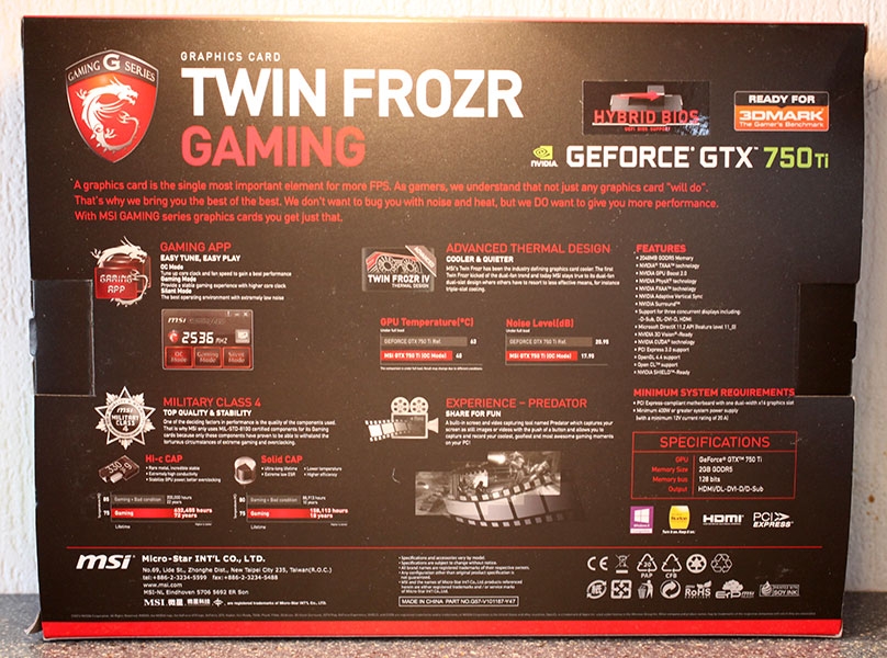
Contents
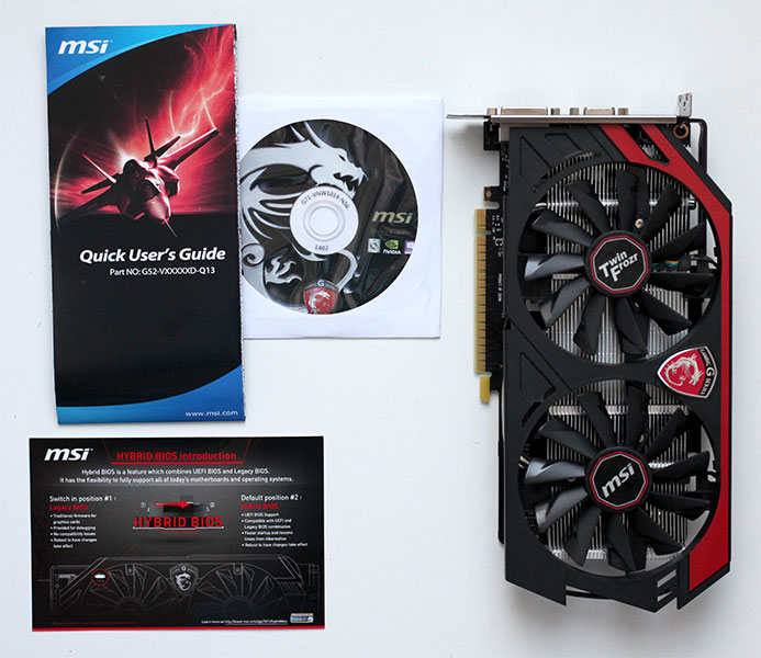
You will receive:
- Graphics card
- Driver CD + documentation
Our Patreon Silver Supporters can read articles in single-page format.
Apr 13th, 2025 10:03 EDT
change timezone
Latest GPU Drivers
New Forum Posts
- Upgrade for a GTX-1060 video card to a X570 AM4 MB w/ a Ryzen 9 3900X (16)
- RX 9000 series GPU Owners Club (298)
- Lenovo Workstations Owners Club (43)
- How to relubricate a fan and/or service a troublesome/noisy fan. (211)
- Is RX 9070 VRAM temperature regular value or hotspot? (352)
- Advice on GPU upgrade (8)
- Share your AIDA 64 cache and memory benchmark here (3051)
- TPU's Nostalgic Hardware Club (20236)
- SK hynix A-Die (Overclocking thread) only for RYZEN AM5 users (27)
- ASRock Z590 OC Formula. (29)
Popular Reviews
- Thermaltake TR100 Review
- The Last Of Us Part 2 Performance Benchmark Review - 30 GPUs Compared
- TerraMaster F8 SSD Plus Review - Compact and quiet
- Zotac GeForce RTX 5070 Ti Amp Extreme Review
- ASUS GeForce RTX 5080 TUF OC Review
- ASRock Z890 Taichi OCF Review
- Sapphire Radeon RX 9070 XT Pulse Review
- Sapphire Radeon RX 9070 XT Nitro+ Review - Beating NVIDIA
- Upcoming Hardware Launches 2025 (Updated Apr 2025)
- MSI MAG CORELIQUID A15 360 Review
Controversial News Posts
- NVIDIA GeForce RTX 5060 Ti 16 GB SKU Likely Launching at $499, According to Supply Chain Leak (181)
- MSI Doesn't Plan Radeon RX 9000 Series GPUs, Skips AMD RDNA 4 Generation Entirely (146)
- Microsoft Introduces Copilot for Gaming (124)
- NVIDIA Sends MSRP Numbers to Partners: GeForce RTX 5060 Ti 8 GB at $379, RTX 5060 Ti 16 GB at $429 (122)
- Nintendo Confirms That Switch 2 Joy-Cons Will Not Utilize Hall Effect Stick Technology (105)
- Over 200,000 Sold Radeon RX 9070 and RX 9070 XT GPUs? AMD Says No Number was Given (100)
- Nintendo Switch 2 Launches June 5 at $449.99 with New Hardware and Games (99)
- NVIDIA PhysX and Flow Made Fully Open-Source (77)