 32
32
MSI Z77A-GD65 GAMING Intel LGA 1155 Review
Overclocking Performance Summary »Overclocking - The Hardware


Although MSI has made it pretty clear that the Z77 MPower board is their "top overclocker", the MSI Z77A-GD65 GAMING includes a fair number of overclocking features. First and foremost, the Z77A-GD65 GAMING board is fitted with dual BIOS chips, great for easy recovery from a failed overclock, especially since you can swap between the BIOSes easily using the onboard switch. There is an LED above each individual BIOS chip to indicate which is in use, and a dual-digit LED POST display is right next to the BIOS chips to help diagnose a failed boot attempt. The POST display LEDs automatically swap over to display CPU temperatures once the POST process has completed, a handy feature I actually didn't find any documentation for, nor were the options to enable or disable this function obvious in the BIOS.

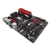
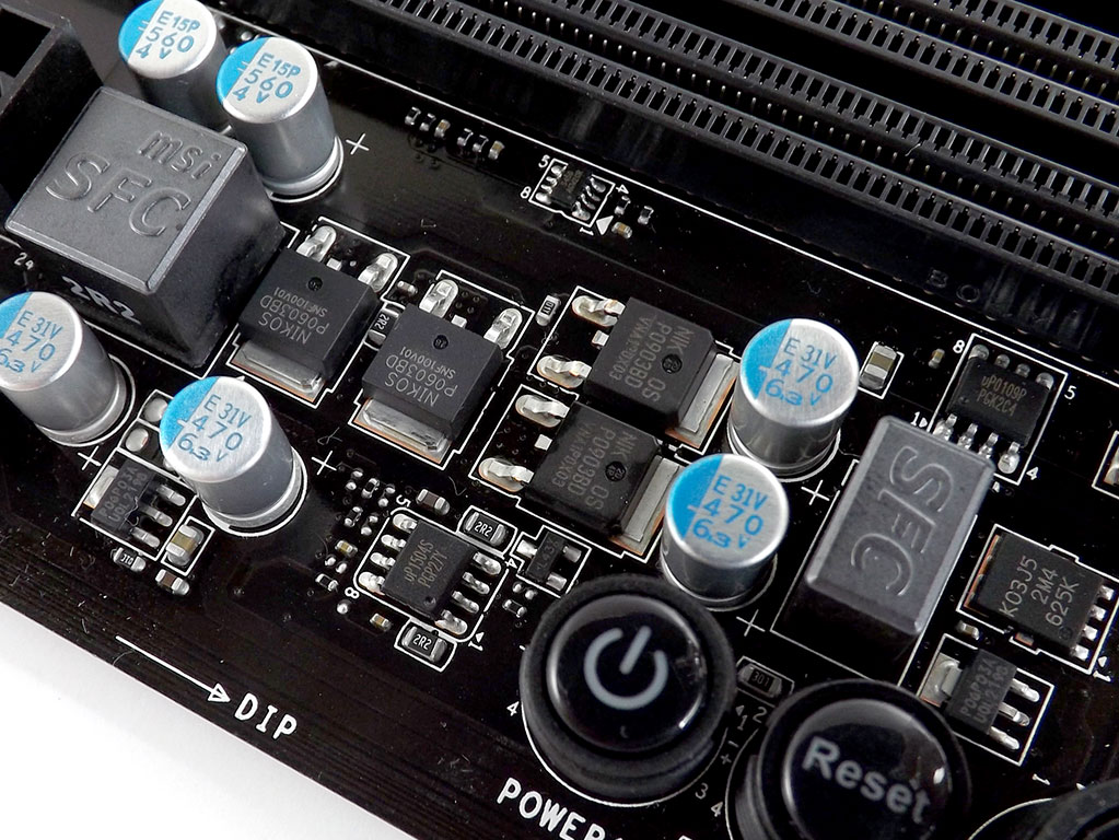
There are also a set of three buttons near the top-right edge of the board, near the DIMM slots. Two buttons are used for ON/OFF and RESET, while the third, labeled "OC Genie", enables the 4.2 GHz overclock that was mentioned on the "MTC" testing certificate that I found in the box. There is also a pin block just south of those buttons for you to plug the V-Check cables into, to monitor critical system voltages in real-time using a digital multimeter.
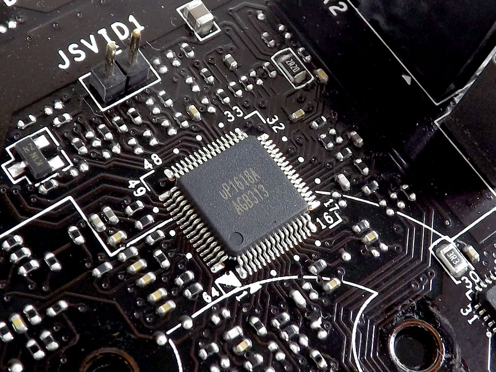
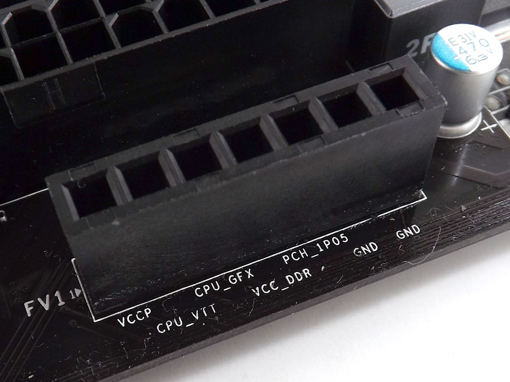
The board's VRM is controlled by a UPI Semi control chip, which manages all the CPU phases that are on either side of it. Just above the DIMM slots are a series of LEDs to indicate which of the main eight phases are in use; they will flicker on and off as each phase is utilized.
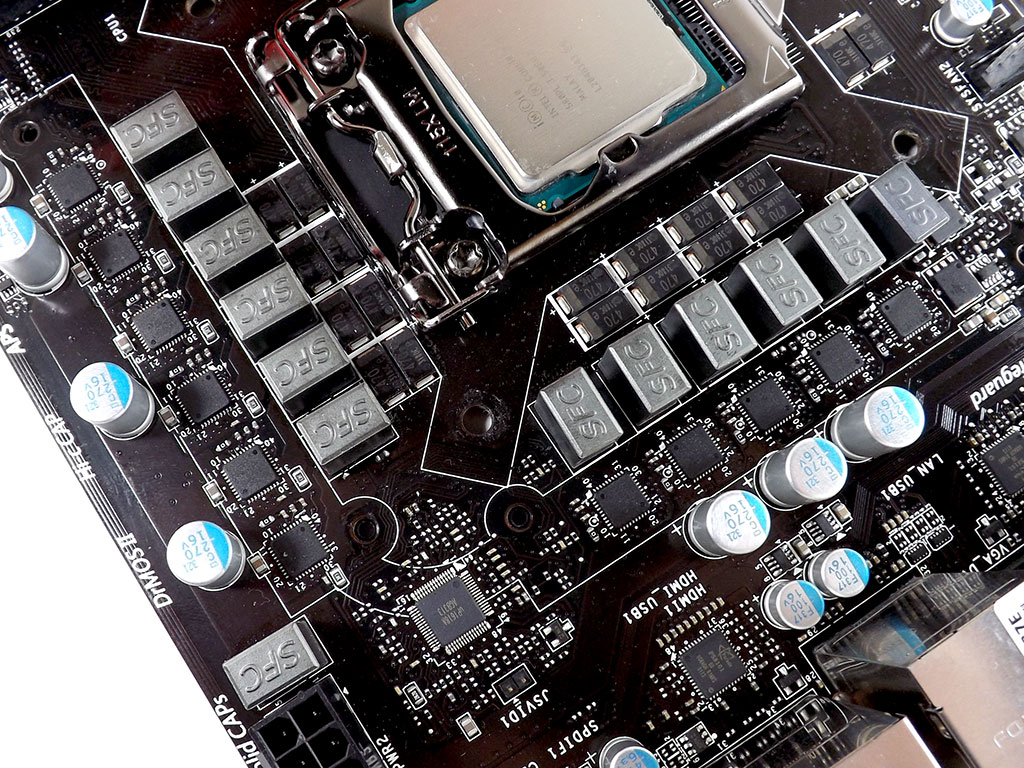
Looking closely at the VRM design with the dragon-shaped heatsinks removed, I found eleven DRMOS components as well as several other MOSFETS, so, honestly, I'm not sure what's going on here. The DRMOS LEDs indicate eight phases, but here are eleven phases...or twelve? Either way, it's more than enough to keep high overclocks powered well, as I barely noticed the VRM cooler getting warm to the touch during overclock testing. The DIMM VRM was equally perplexing. Seemingly a hybrid dual-phase design with both a single input and output, it had no issues pushing my G.Skill test DIMMs to 2666 MHz and beyond.
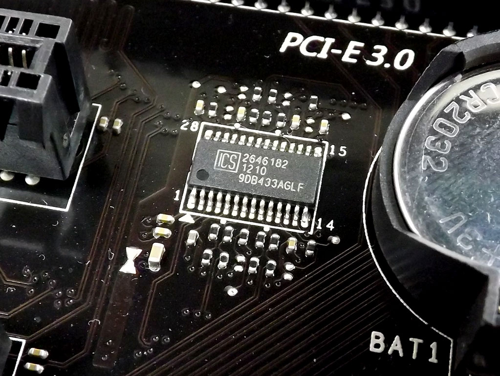

There's an ICS PLL between the PCIe slots to help stabilize clocks given to each slot. I found a Fintek F71889AD chip to be providing temperature and voltage monitoring; it also provides the high-speed PS/2 port found on the rear I/O plate.
Feb 7th, 2025 11:15 EST
change timezone
Latest GPU Drivers
New Forum Posts
- Free Games Thread (4432)
- NVCleanstall not launching, giving a dll error (0)
- Help me decide..........OLED monitors (5)
- AM4 and Combining Different RAM? (56)
- Post your Monster Hunter Wilds benchmark scores (59)
- RTX 2070 Super build (68)
- X79 and/or rampage IV OC'ing thread for those of us still left.... (2378)
- Power Throttling with no limited power (3)
- Opinions on AI (427)
- Modified drivers for X-Fi sound cards. (21)
Popular Reviews
- Kingdom Come Deliverance II Performance Benchmark Review - 35 GPUs Tested
- Spider-Man 2 Performance Benchmark Review - 35 GPUs Tested
- Corsair Frame 4000D Review
- Formovie Cinema Edge 4K UST Laser Projector Review
- ASUS ROG Harpe Ace Extreme Review
- NVIDIA GeForce RTX 5080 Founders Edition Review
- Kingdom Come: Deliverance 2 Handheld Performance Review
- Gigabyte GeForce RTX 5080 Gaming OC Review
- MSI GeForce RTX 5080 Vanguard SOC Review
- AMD Ryzen 7 9800X3D Review - The Best Gaming Processor
Controversial News Posts
- AMD Radeon 9070 XT Rumored to Outpace RTX 5070 Ti by Almost 15% (285)
- AMD is Taking Time with Radeon RX 9000 to Optimize Software and FSR 4 (256)
- AMD Denies Radeon RX 9070 XT $899 USD Starting Price Point Rumors (239)
- Edward Snowden Lashes Out at NVIDIA Over GeForce RTX 50 Pricing And Value (235)
- AMD Radeon RX 9070 XT & RX 9070 Custom Models In Stock at European Stores (226)
- New Leak Reveals NVIDIA RTX 5080 Is Slower Than RTX 4090 (215)
- AMD's Radeon RX 9070 Launch Faces Pricing Hurdles (175)
- AMD Radeon RX 9070 XT Tested in Cyberpunk 2077 and Black Myth: Wukong (169)