 80
80
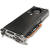
NVIDIA GeForce GTX 650 Ti Boost 2 GB Review
(80 Comments) »Introduction
It has been less than a week since a major GPU launch, AMD's Radeon HD 7790, and we already have one from NVIDIA, the GeForce GTX 650 Ti Boost. When AMD announced the Radeon HD 7950 Boost Edition in August 2012, reacting to stiff competition from NVIDIA's GeForce GTX 660 Ti, there wasn't much to lose if a consumer overlooked the "Boost" component while making the purchase, just higher clock speeds and PowerTune with Boost. The GeForce GTX 650 Ti Boost, launched today, is an extremely different beast to the original GTX 650 Ti it shares most of its name with.

NVIDIA launched the original GeForce GTX 650 Ti in October 2012 to capture the $150 price-point. The card comprehensively beat AMD's $120 Radeon HD 7770 GHz Edition in performance, which forced AMD to carve a $180 1 GB variant out of its Radeon HD 7850 that is armed with 2 GB of memory for around $210. Even as AMD carried on for six months with a gaping hole between the HD 7770 and HD 7850—a hole filled by the HD 7790 just last week—NVIDIA dug itself a hole of its own between the $150 GeForce GTX 650 Ti and the GeForce GTX 660, giving the two HD 7850 variants a free hand in the sub-$200 market, but the company rolled out the GeForce GTX 650 Ti Boost to fill exactly that gap.
Strategically priced at $170 for the 2 GB variant, with a possibility of a $150 1 GB variant in the near future, the new GeForce GTX 650 Ti Boost has its eyes set on rattling AMD's sub-$200 stronghold. So what exactly gives the "Boost" superhero powers over the GTX 650 Ti? The answer lies in the silicon. The original GTX 650 Ti uses a significantly cut down version of the 28 nm GK106 silicon. It only features 80 percent of the chip's available streaming multiprocessors, a 33% narrower memory bus, unimpressive sub-gigahertz GPU clock speed, and lacks GPU Boost—a well-implemented dynamic overclocking technology. The GeForce GTX 650 Ti Boost doesn't tinker with the streaming multiprocessor count, but utilizes the full 192-bit wide GDDR5 memory interface, GPU Boost with core clock speeds crossing the 1 GHz mark far too often, and a memory bandwidth of 144 GB/s. These three subtle changes, along with a PCB/cooler design similar to that of the GeForce GTX 660, gives the card a more premium-feel in the sub-$200 market.


The GeForce GTX 650 Ti Boost, based on the "Kepler" GPU micro-architecture, features four of the silicon's five streaming multiprocessors, which amounts to 768 CUDA cores, 64 texture memory units (TMUs), 24 raster operations processors (ROPs), and a 192-bit wide memory interface. 2 GB is the standard memory amount for now. The core features a nominal clock speed of 980 MHz that can boost itself to 1033 MHz; most real-world gaming and creativity apps should have no problems letting the chip run at that speed. The memory is clocked at 6008 MHz (GDDR5-effective), which translates into a decent 144 GB/s memory bandwidth.

In this review, we test the NVIDIA reference design GeForce GTX 650 Ti Boost. It bears an uncanny resemblance to reference boards of the GTX 660, GTX 660 Ti, and GTX 670, giving you that premium feel inside your rig.
| GeForce GTX 650 Ti | GeForce GTX 560 | Radeon HD 6870 | GeForce GTX 560 Ti | Radeon HD 7790 | Radeon HD 6950 | GeForce GTX 570 | Radeon HD 6970 | Radeon HD 7850 | GeForce GTX 650 Ti Boost | GeForce GTX 660 | Radeon HD 7870 | GeForce GTX 580 | GeForce GTX 660 Ti | |
|---|---|---|---|---|---|---|---|---|---|---|---|---|---|---|
| Shader Units | 768 | 336 | 1120 | 384 | 896 | 1408 | 480 | 1536 | 1024 | 768 | 960 | 1280 | 512 | 1344 |
| ROPs | 16 | 32 | 32 | 32 | 16 | 32 | 40 | 32 | 32 | 24 | 24 | 32 | 48 | 24 |
| Graphics Processor | GK106 | GF114 | Barts | GF114 | Bonaire | Cayman | GF110 | Cayman | Pitcairn | GK106 | GK106 | Pitcairn | GF110 | GK104 |
| Transistors | 2540M | 1950M | 1700M | 1950M | 2080M | 2640M | 3000M | 2640M | 2800M | 2540M | 2540M | 2800M | 3000M | 3500M |
| Memory Size | 1024 MB | 1024 MB | 1024 MB | 1024 MB | 1024 MB | 2048 MB | 1280 MB | 2048 MB | 2048 MB | 2048 MB | 2048 MB | 2048 MB | 1536 MB | 2048 MB |
| Memory Bus Width | 128 bit | 256 bit | 256 bit | 256 bit | 128 bit | 256 bit | 320 bit | 256 bit | 256 bit | 192 bit | 192 bit | 256 bit | 384 bit | 192 bit |
| Core Clock | 925 MHz | 810 MHz | 900 MHz | 823 MHz | 1000 MHz | 800 MHz | 732 MHz | 880 MHz | 860 MHz | 980 MHz+ | 980 MHz+ | 1000 MHz | 772 MHz | 915 MHz+ |
| Memory Clock | 1350 MHz | 1002 MHz | 1050 MHz | 1002 MHz | 1500 MHz | 1250 MHz | 950 MHz | 1375 MHz | 1200 MHz | 1502 MHz | 1502 MHz | 1200 MHz | 1002 MHz | 1502 MHz |
| Price | $140 | $170 | $170 | $200 | $150 | $170 | $250 | $380 | $180 | $170 | $215 | $220 | $310 | $280 |
The Card
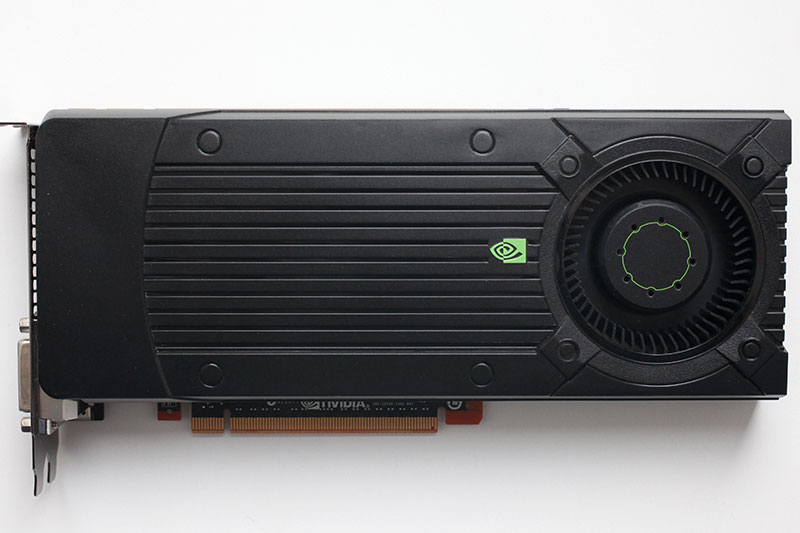
NVIDIA's GeForce GTX 650 Ti Boost reference design looks exactly like the GTX 660/670 reference design. The card is 24 cm long and 11.5 cm high.

Installing the card requires two slots in your system.
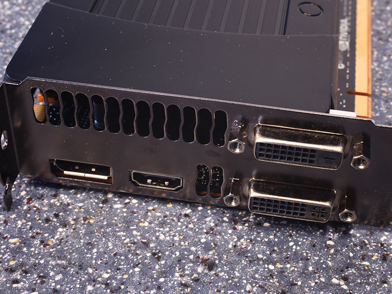
Display connectivity options include two DVI ports, one full-size DisplayPort, and one full-size HDMI port. You may use all outputs at the same time, so triple-monitor surround gaming is possible with one card.
The GPU also includes an HDMI sound device. It is HDMI 1.4a compatible, which includes HD audio and Blu-ray 3D movies support.
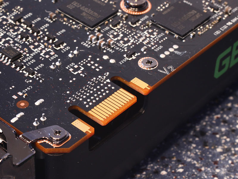
A single SLI connector is available, which means you can combine up to two cards for a multi-GPU setup. SLI was not supported at all on the GTX 650 Ti without Boost.


Pictured above are the front and back, showing the disassembled board. High-res versions are also available (front, back). If you choose to use these images for voltmods, etc., please include a link back to this site, or let us post your article.
A Closer Look


NVIDIA's cooler is reasonably simple. A large slab of metal with a copper base handles any heat produced by the GPU.
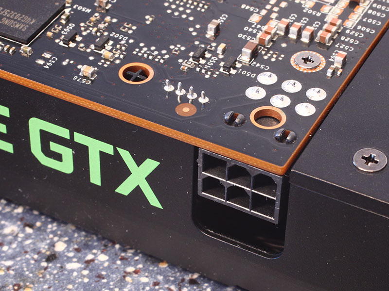
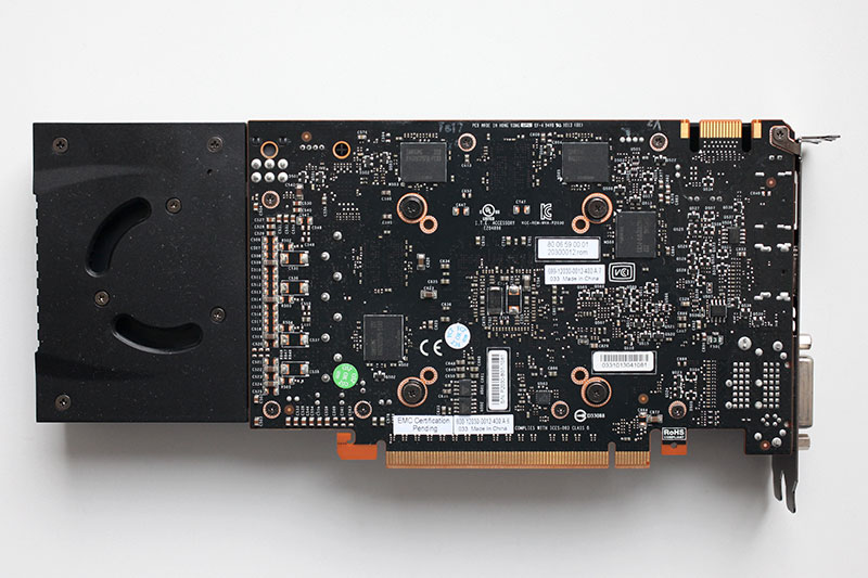
The card requires a single 6-pin PCI-Express power cable for operation. This power configuration is good for up to 150 W of power draw.

NVIDIA uses an OnSemi NCP5395 voltage controller. We have seen this controller on many designs before. It is a cost effective solution that does not provide any I2C, so advanced monitoring is not possible.

The GDDR5 memory chips are made by Samsung and carry the model number K4G20325FD-FC03. They are specified to run at 1500 MHz (6000 MHz GDDR5 effective).

NVIDIA's GK106 processor is produced on a 28 nm at TSMC, Taiwan. The transistor count is 2.54 billion.
Test System
| Test System - VGA Rev. 25 | |
|---|---|
| Processor: | Intel Core i7-3770K @ 4.6 GHz (Ivy Bridge, 8192 KB Cache) |
| Motherboard: | ASUS Maximus V Gene Intel Z77 |
| Memory: | 2x 4096 MB Corsair Vengeance PC3-12800 DDR3 @ 1600 MHz 9-9-9-24 |
| Harddisk: | WD Caviar Blue WD5000AAKS 500 GB |
| Power Supply: | Antec HCP-1200 1200W |
| Software: | Windows 7 64-bit Service Pack 1 |
| Drivers: | NVIDIA: 310.70 WHQL ATI: Catalyst 13.1 WHQL GTX 650 Ti Boost: 314.21 Beta |
| Display: | LG Flatron W3000H 30" 2560x1600 3x Hanns.G HL225DBB 21.5" 1920x1080 |
- All video card results were obtained on this exact system with exactly the same configuration.
- All games were set to their highest quality setting unless indicated otherwise.
- AA and AF are applied via in-game settings, not via the driver's control panel.
- 1280 x 800, 2x Anti-aliasing. Common resolution for most smaller flatscreens today (17" - 19"). A bit of eye candy turned on in the drivers.
- 1680 x 1050, 4x Anti-aliasing. Most common widescreen resolution on larger displays (19" - 22"). Very good looking driver graphics settings.
- 1920 x 1200, 4x Anti-aliasing. Typical widescreen resolution for large displays (22" - 26"). Very good looking driver graphics settings.
- 2560 x 1600, 4x Anti-aliasing. Highest possible resolution for commonly available displays (30"). Very good looking driver graphics settings.
Our Patreon Silver Supporters can read articles in single-page format.
Apr 28th, 2025 22:22 EDT
change timezone
Latest GPU Drivers
New Forum Posts
- Never buying an AOC or AOpen branded monitor ever again, here is my experience. (9)
- What's your latest tech purchase? (23655)
- Why does the "Link Rate (current)" in my GPU-Z show 60G? (0)
- The TPU UK Clubhouse (26178)
- Antec 1200 replacement but for EATX motherboards? (3)
- Is my ASUS Astral 5090 Safe? Red Light blinking while gaming (2)
- Thermaltake riing plus 12 rgb and other rgb fans. (11)
- M18R2 4080 (5)
- Are the 8 GB cards worth it? (406)
- Random Entire System Stutter when using Throttlestop (9)
Popular Reviews
- Clair Obscur: Expedition 33 Performance Benchmark Review - 33 GPUs Tested
- Oblivion Remastered Handheld Performance Review
- NVIDIA GeForce RTX 5060 Ti 8 GB Review - So Many Compromises
- ASUS GeForce RTX 5090 Astral Liquid OC Review - The Most Expensive GPU I've Ever Tested
- Crucial CUDIMM DDR5-6400 128 GB CL52 Review
- Upcoming Hardware Launches 2025 (Updated Apr 2025)
- Sapphire Radeon RX 9070 XT Pulse Review
- Sapphire Radeon RX 9070 XT Nitro+ Review - Beating NVIDIA
- AMD Ryzen 7 9800X3D Review - The Best Gaming Processor
- NVIDIA GeForce RTX 5070 Founders Edition Review
Controversial News Posts
- NVIDIA GeForce RTX 5060 Ti 16 GB SKU Likely Launching at $499, According to Supply Chain Leak (182)
- NVIDIA Sends MSRP Numbers to Partners: GeForce RTX 5060 Ti 8 GB at $379, RTX 5060 Ti 16 GB at $429 (127)
- NVIDIA Launches GeForce RTX 5060 Series, Beginning with RTX 5060 Ti This Week (115)
- Nintendo Confirms That Switch 2 Joy-Cons Will Not Utilize Hall Effect Stick Technology (105)
- Nintendo Switch 2 Launches June 5 at $449.99 with New Hardware and Games (99)
- Sony Increases the PS5 Pricing in EMEA and ANZ by Around 25 Percent (84)
- NVIDIA PhysX and Flow Made Fully Open-Source (82)
- Parts of NVIDIA GeForce RTX 50 Series GPU PCB Reach Over 100°C: Report (77)