 172
172
NVIDIA GeForce RTX 3070 Founders Edition Review - Disruptive Price-Performance
(172 Comments) »Introduction
NVIDIA GeForce RTX 3070 "Ampere" is the third new graphics card launch from the RTX 30-series, and possibly the most important one so far. The company debuted the GeForce "Ampere" graphics card family with the $700 RTX 3080 and $1,500 RTX 3090 in quick succession, and we today have the $500 GeForce RTX 3070 Founders Edition for review. Owing to its attractive price, this card is expected to sell in droves given how successful the RTX 2070 Super and RX 5700 XT are. As we get to the bottom of NVIDIA's pyramidal product stack, we'll see products that sell in larger volumes. Still, the RTX 3070 is a highly important product as it's designed to offer AAA gaming with RTX-on at the growingly popular 1440p resolution and is 4K-capable, as well as the gateway to the high-end segment. Consider the RTX 3070 to be the BMW 3-series for "Ampere," which, despite the 5 and 7-series being around, remains eminently desirable if it can deliver.
With the GeForce RTX 3070, NVIDIA is releasing its second largest GeForce "Ampere" silicon, the 8 nm "GA104." It has lighter specifications than the RTX 3080, but its SIMD muscle is double that of its predecessor, the RTX 2070. In fact, right in its launch event, NVIDIA claimed that the RTX 3070 is faster than the RTX 2080 Ti, the previous-generation flagship card that retailed at well over $1000. This would mean the RTX 3070 isn't just capable of maxed-out gaming with RTX raytracing at 1440p, but also 4K Ultra HD gaming with fairly high settings. One could also expect high refresh-rate (>120 Hz) e-sports gaming at Full HD resolution to be one of the RTX 3070's core use-cases given the RTX 2080 Ti fits this bill.

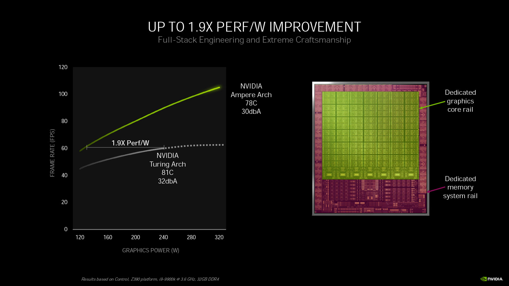
The "Ampere" graphics architecture heralds the 2nd generation of NVIDIA's groundbreaking RTX technology, which introduces real-time raytracing to the gaming segment. NVIDIA figured out a way to combine conventional raster 3D graphics with raytraced components, such as lighting, shadows, reflections, ambient-occlusion, global illumination, and, with "Ampere," even raytraced motion blur—a difficult effect to pull off in real time. 2nd generation RTX is a combination of the new "Ampere" CUDA core that nearly doubles the compute throughput over the previous generation "Turing" by implementing full concurrent INT32+FP32 math operations; the second generation RT core, which has double the intersection throughput as previous generation and introduces new hardware to accelerate raytraced motion-blur; and the 3rd generation Tensor core, which leverages the sparsity phenomenon in deep-learning neural nets to increase AI inference performance by an order of magnitude.
As we mentioned earlier, the GeForce RTX 3070 in this review is based on the "GA104" silicon with 46 of 48 streaming multiprocessors (23 out of 24 TPCs) enabled, amounting to a staggering 5,888 "Ampere" CUDA cores, 184 third generation Tensor cores, 46 RT cores, and 184 TMUs. There's a 50% increase in raster performance because of 96 ROPs, instead of the 64 on the RTX 2070. The memory sub-system surprisingly hasn't changed over the previous generation. You still get 8 GB of conventional GDDR6 memory across a 256-bit wide memory interface. It still ticks at 14 Gbps, which amounts to the same 448 GB/s bandwidth. No GDDR6X magic to be had here, NVIDIA had to cut costs somewhere to sell this card at $500. The card's typical board power is rated at 220 W, which may be much higher than the 185 W of the RTX 2070, but is significantly lower than the 320 W of the RTX 3080. This also means that custom-design RTX 3070 cards can make do with single 8-pin PCIe power inputs if the board partners chooses.
Our NVIDIA GeForce RTX 3070 Founders Edition graphics card review covers this beautiful card, which is designed in-house by NVIDIA. The Founders Edition isn't intended to serve as a reference design, but, rather, an above baseline implementation of the silicon by NVIDIA; a reference-design serves as a baseline for board partners to better with their custom designs. The Founders Edition card is designed to raise the bar for custom-design cards to catch up with. The card uses the same "dual-axial flow-through" cooler design philosophy as the RTX 3080 and RTX 3090 Founders Edition cards, but with both the fans on the same side. The second fan still moves air through the card because of a large cutout in the backplate. NVIDIA also retained the space-saving 12-pin power input despite the fact that with a board power of 220 W, a single 8-pin connector would have sufficed. The included 12-pin to 8-pin adapter only has one 8-pin input.
In this review, we take the NVIDIA GeForce RTX 3070 Founders Edition for a spin and test the company's claim of the card being faster than the RTX 2080 Ti, and how it changes the performance-segment landscape. If the claim holds, this would be the first performance-segment card from NVIDIA to beat a previous-generation flagship since 2016 "Pascal."
| Price | Shader Units | ROPs | Core Clock | Boost Clock | Memory Clock | GPU | Transistors | Memory | |
|---|---|---|---|---|---|---|---|---|---|
| RX 5700 | $330 | 2304 | 64 | 1465 MHz | 1625 MHz | 1750 MHz | Navi 10 | 10300M | 8 GB, GDDR6, 256-bit |
| GTX 1080 | $330 | 2560 | 64 | 1607 MHz | 1733 MHz | 1251 MHz | GP104 | 7200M | 8 GB, GDDR5X, 256-bit |
| RTX 2060 Super | $380 | 2176 | 64 | 1470 MHz | 1650 MHz | 1750 MHz | TU106 | 10800M | 8 GB, GDDR6, 256-bit |
| RX Vega 64 | $400 | 4096 | 64 | 1247 MHz | 1546 MHz | 953 MHz | Vega 10 | 12500M | 8 GB, HBM2, 2048-bit |
| GTX 1080 Ti | $650 | 3584 | 88 | 1481 MHz | 1582 MHz | 1376 MHz | GP102 | 12000M | 11 GB, GDDR5X, 352-bit |
| RX 5700 XT | $370 | 2560 | 64 | 1605 MHz | 1755 MHz | 1750 MHz | Navi 10 | 10300M | 8 GB, GDDR6, 256-bit |
| RTX 2070 | $340 | 2304 | 64 | 1410 MHz | 1620 MHz | 1750 MHz | TU106 | 10800M | 8 GB, GDDR6, 256-bit |
| RTX 2070 Super | $450 | 2560 | 64 | 1605 MHz | 1770 MHz | 1750 MHz | TU104 | 13600M | 8 GB, GDDR6, 256-bit |
| Radeon VII | $680 | 3840 | 64 | 1802 MHz | N/A | 1000 MHz | Vega 20 | 13230M | 16 GB, HBM2, 4096-bit |
| RTX 2080 | $600 | 2944 | 64 | 1515 MHz | 1710 MHz | 1750 MHz | TU104 | 13600M | 8 GB, GDDR6, 256-bit |
| RTX 2080 Super | $690 | 3072 | 64 | 1650 MHz | 1815 MHz | 1940 MHz | TU104 | 13600M | 8 GB, GDDR6, 256-bit |
| RTX 2080 Ti | $1000 | 4352 | 88 | 1350 MHz | 1545 MHz | 1750 MHz | TU102 | 18600M | 11 GB, GDDR6, 352-bit |
| RTX 3070 | $500 | 5888 | 96 | 1500 MHz | 1725 MHz | 1750 MHz | GA104 | 17400M | 8 GB, GDDR6, 256-bit |
| RTX 3080 | $700 | 8704 | 96 | 1440 MHz | 1710 MHz | 1188 MHz | GA102 | 28000M | 10 GB, GDDR6X, 320-bit |
| RTX 3090 | $1500 | 10496 | 112 | 1395 MHz | 1695 MHz | 1219 MHz | GA102 | 28000M | 24 GB, GDDR6X, 384-bit |
The GeForce Ampere Architecture
Earlier this year, on September 5, we did a comprehensive article on the NVIDIA GeForce Ampere graphics architecture, along with a deep-dive into the key 2nd Gen RTX technology and various other features NVIDIA is introducing that are relevant to gaming. Be sure to check out that article for more details.

The GeForce Ampere architecture is the first time NVIDIA both converged and diverged its architecture IP between graphics and compute processors. Back in May, NVIDIA debuted Ampere on its A100 Tensor Core compute processor targeted at AI and HPC markets. The A100 Tensor Core is a headless compute chip that lacks all raster graphics components, so NVIDIA could cram in the things relevant to the segment. The GeForce Ampere, however, is a divergence with a redesigned streaming multiprocessor different from that of the A100. These chips have all the raster graphics hardware, display and media acceleration engines, and, most importantly, the 2nd generation RT core that accelerates real-time raytracing. A slightly slimmed down version of the 3rd generation tensor core of the A100 also gets carried over. NVIDIA sticks to using GDDR-type memory over expensive memory architectures, such as HBM2E.
NVIDIA pioneered real-time raytracing on consumer graphics hardware, and three key components make the NVIDIA RTX technology work: the SIMD components, aka CUDA cores, the RT cores, which do the heavy lifting with raytracing, calculating BVH traversal and intersections, and tensor cores, which are hardware components accelerating AI deep-learning neural net building and training. NVIDIA uses an AI-based denoiser for RTX. With Ampere, NVIDIA is introducing new generations of the three components, with the objective being to reduce the performance cost of RTX, and nearly double performance over generations. These include the new Ampere streaming multiprocessor that more than doubles FP32 throughput over generations, the 2nd Gen RT core that features hardware that enables new RTX effects, such as raytraced motion blur, and the 3rd generation tensor core, which leverages sparsity in DNNs to increase AI inference performance by an order of magnitude.
GA104 GPU and Ampere SM

The GeForce RTX 3070 is the first graphics card to implement the company's new "GA104" Ampere silicon, the second largest chip based on the GeForce "Ampere" graphics architecture. Unlike the past few generations of GeForce, in which the xx80-series SKU maxed out the Gx104-series silicon, with the xx70-series SKU being heavily cut down, the new GeForce RTX 3070 nearly maxes out the "GA104" since the RTX 3080 is based on the much larger "GA102." The new "GA104" chip is built on the same 8 nm silicon fabrication process by Samsung as the "GA102." Its die crams in 17.4 billion transistors, a figure which is only slightly short of the 18.6 billion of the previous-generation flagship "TU102," but over 10 billion short of the "GA102." The die-area measures 392.5 mm².
The GA104 silicon features a largely similar component hierarchy to past-generation NVIDIA GPUs, but with the bulk of engineering effort focused on the new Ampere Streaming Multiprocessor (SM). The GPU supports the PCI-Express 4.0 x16 host interface, which doubles the host interface bandwidth over PCI-Express 3.0 x16. With this generation, NVIDIA is also relegating SLI and the NVLink interface to only the top-dog RTX 3090, even the RTX 3080 loses out on it. Also, unlike the "GA102," the "GA104," at least in its RTX 3070 avatar, loses out on the blazing fast GDDR6X memory standard. It features the same 256-bit wide memory interface driving conventional GDDR6.
The GA104 silicon features six graphics processing clusters (GPCs), the mostly independent subunits of the GPU. Each GPC has four texture processing clusters (TPCs), the indivisible subunit that is the main number-crunching muscle of the GPU (unlike six TPCs per GPC on the "GA102). One random TPCs is disabled to carve out the RTX 3070. Each TPC shares a PolyMorph engine between two streaming multiprocessors (SMs). The SM is what defines the generation and where the majority of NVIDIA's engineering effort is localized. The Ampere SM crams in 128 CUDA cores, double that of the 64 CUDA cores in the Turing SM.
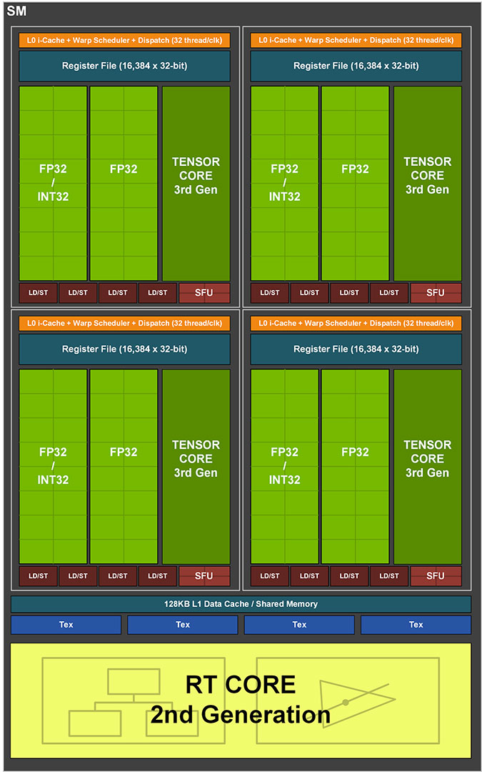

Each GeForce Ampere SM features four processing blocks that each share an L1I cache, warp scheduler, and a register file among 128 CUDA cores. From these, 64 can handle concurrent FP32 and INT32 math operations, while 64 are pure FP32. Each cluster also features a 3rd generation Tensor Core. At the SM level, the four processing blocks share a 128 KB L1D cache that also serves as shared memory; four TMUs and a 2nd generation RT core. As we mentioned, each processing block features two FP32 data paths; one of these consists of CUDA cores that can execute 16 FP32 operations per clock cycle, while the other data path consists of CUDA cores capable of 16 FP32 and 16 INT32 concurrent operations per clock. Each SM also features a tiny, unspecified number of rudimentary FP64 cores, which work at 1/64 the performance of the FP64 cores on the A100 Tensor Core HPC processor. These FP64 cores are only there so double-precision software doesn't run into compatibility problems.
2nd Gen RT Core, 3rd Gen Tensor Core


NVIDIA's 2nd generation RTX real-time raytracing technology sees the introduction of more kinds of raytraced effects. NVIDIA's pioneering technology involves composing traditional raster 3D scenes with certain raytraced elements, such as lighting, shadows, global illumination, and reflections.
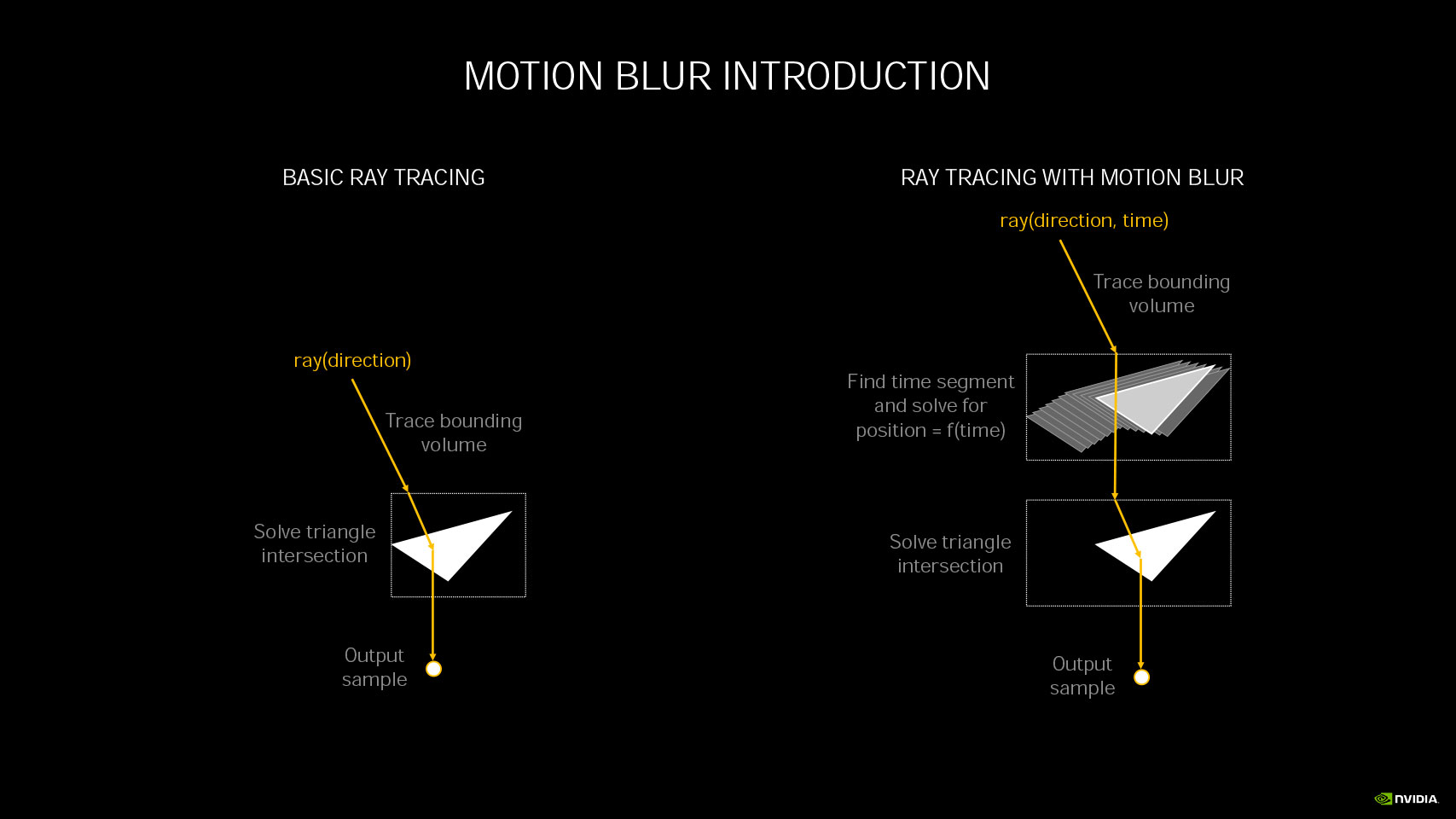
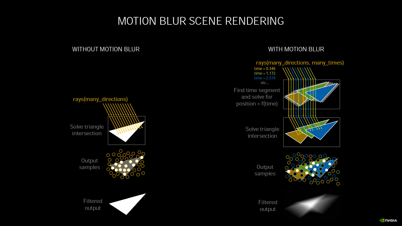
As explained in the Ampere Architecture article, NVIDIA's raytracing philosophy involves heavy bounding volume hierarchy (BVH) traversal, and bounding box/triangle intersection, for which NVIDIA developed a specialized MIMD fixed function in the RT core. Fixed-function hardware handles both the traversal and intersection of rays with bounding boxes or triangles. With the 2nd Gen RT core, NVIDIA is introducing a new component which interpolates triangle position by time. This component enables physically accurate, raytraced motion-blur. Until now, motion-blur was handled as a post-processing effect.
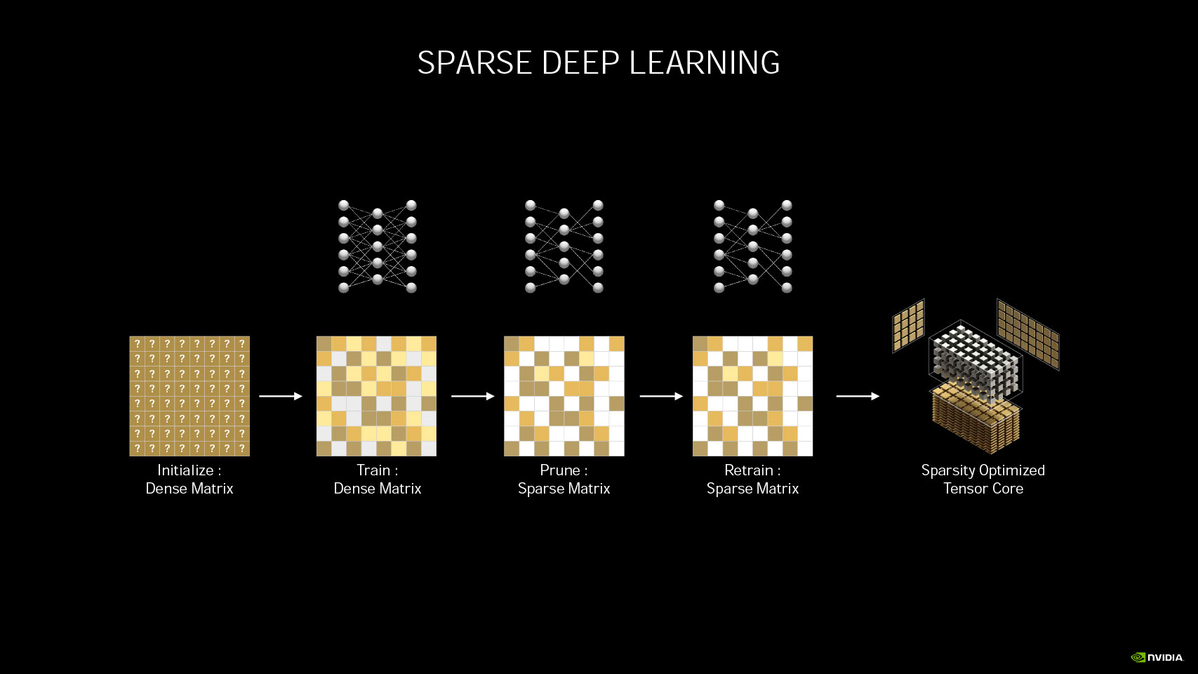
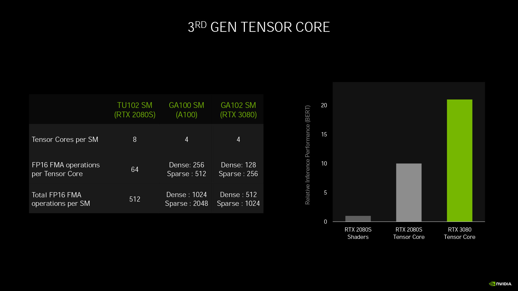
The 3rd generation tensor core sees NVIDIA build on the bulwark of its AI performance leadership, fixed-function hardware designed for tensor math which accelerates AI deep-learning neural-net building and training. AI is heavily leveraged in NVIDIA architectures now, as the company uses an AI-based denoiser for its raytracing architecture and to accelerate technologies such as DLSS. Much like the 3rd generation tensor cores on the company's A100 Tensor Core processor that debuted this Spring, the new tensor cores leverage a phenomenon called sparsity—the ability for a DNN to shed its neural net without losing the integrity of its matrix. Think of this like Jenga: you pull pieces from the middle of a column while the column itself stays intact. The use of sparsity increases AI inference performance by an order of magnitude: 256 FP16 FMA operations in a sparse matrix compared to just 64 on the Turing tensor core, and 1024 sparse FP16 FMA ops per SM compared to 512 on the Turing SM, which has double the tensor core counts.
Display and Media
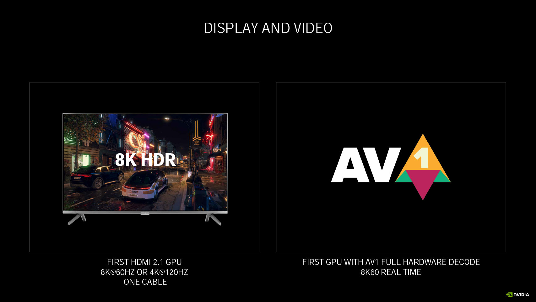
NVIDIA updated the display and media acceleration components of Ampere. To begin with, VirtualLink, or the USB type-C connection, has been removed from the reference design. We've seen no other custom-design cards implement it, so it's safe to assume NVIDIA junked it. The GeForce RTX 3080 puts out three DisplayPort 1.4a, which takes advantage of the new VESA DSC 1.2a compression technology to enable 8K 60 Hz with HDR using a single cable. It also enables 4K at 240 Hz with HDR. The other big development is support for HDMI 2.1, which enables 8K at 60 Hz with HDR, using the same DSC 1.2a codec. NVIDIA claims that DSC 1.2a is "virtually lossless" in quality. The media acceleration features are largely carried over from Turing, except for the addition of AV1 codec hardware decode. As the next major codec to be deployed by the likes of YouTube and Netflix, AV1 is big. It halves the file size over H.265 HEVC for comparable quality. The new H.266 VVC misses out as the standard was introduced too late into Ampere's development.
NVIDIA Ampere Features
Hardware architecture only paints half the story of what's new with GeForce Ampere. Here, we quickly run you through the noteworthy new features introduced by the GeForce RTX 30 series. Some of these will work even with the RTX 20 series through driver updates. When NVIDIA introduced the RTX 20 series Turing, the hot new feature was RTX and real-time raytracing, along with AI acceleration. NVIDIA builds on these with its 2nd generation RTX architecture for vast generational performance improvements. NVIDIA is so confident in the performance uplift that it set its eyes on 8K gameplay. This was probably important as new-generation game consoles, such as the PlayStation 5 and Xbox Series X, formally advertise 4K gaming. High-end gaming PCs can't be seen to play in the same field.
8K is four times the pixels of 4K, or sixteen times Full HD, which is no small ask. Yet NVIDIA believes it can take a crack at 8K by using the new 8K DLSS feature in combination with its new display outputs that support 8K 60 Hz leveraging DSC 1.2a. 8K DLSS renders the game at 1440p and uses a special 9X Super Sampling algorithm to reconstruct details at 8K. NVIDIA demonstrated that this looks better than merely running the game at 8K and making it scale up game assets using bilinear upscaling. The company also listed a large selection of games where frame rates above 8K were obtained.
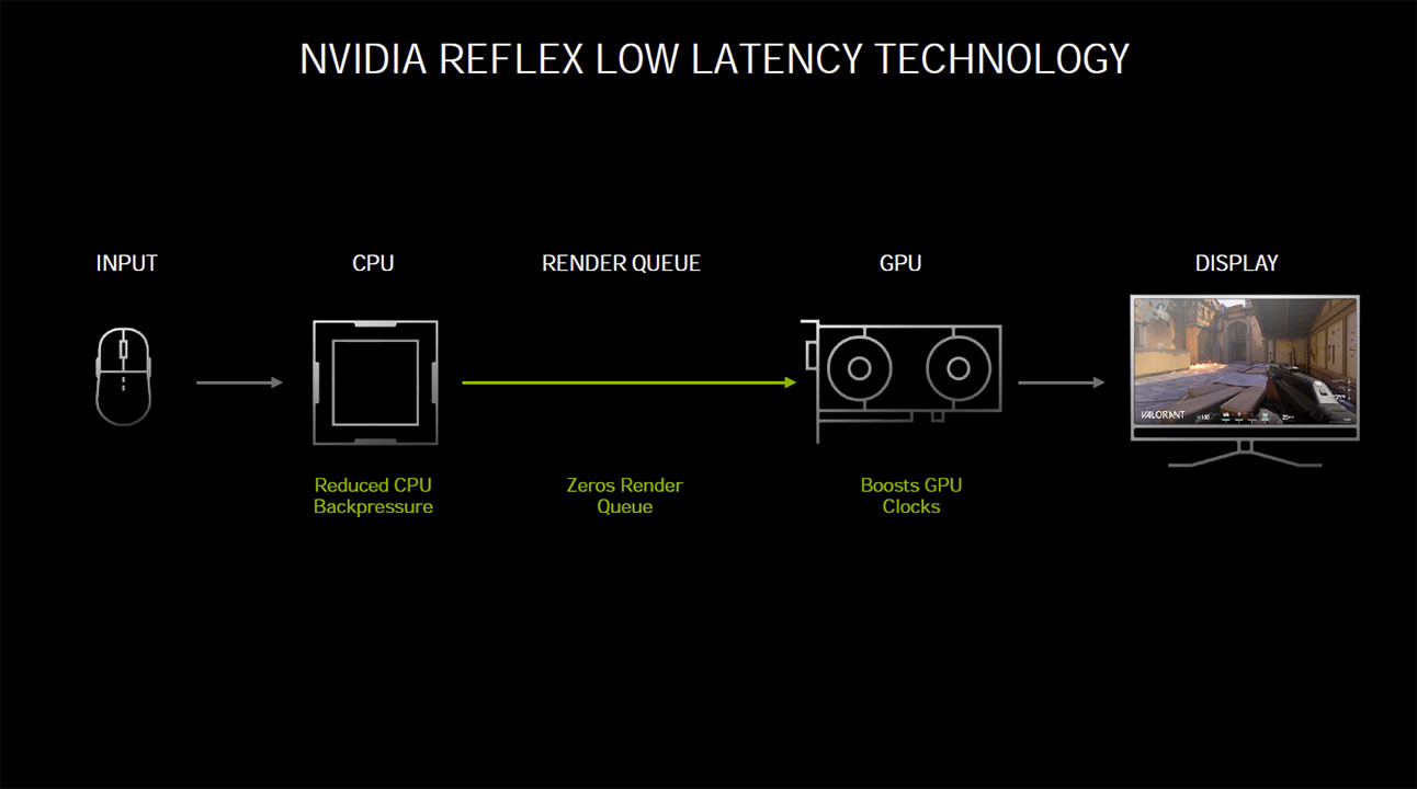
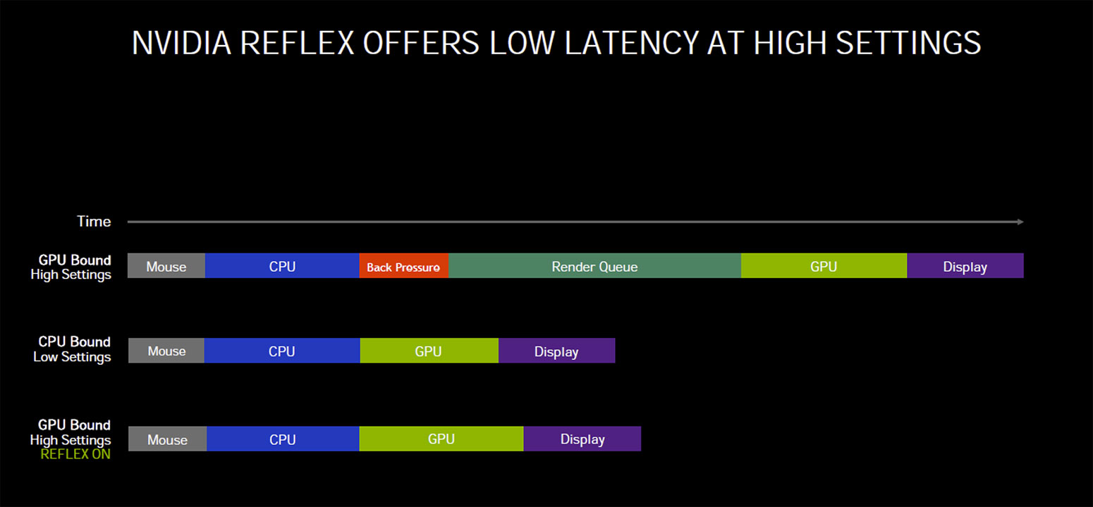
With competitive e-sports gaming that has millions riding on it, it's not enough that network latency is reduced and frame rates increased. NVIDIA discovered that "whole system latency" plays an equally important role as network latency in affecting gamers' competitiveness. System latency is defined by NVIDIA as the time it takes for you to physically click a button on your mouse and for the click to register in-game as an action. In the heat of gameplay, system latency can mean the difference between scoring a hit against the opponent or their getting away. NVIDIA Reflex is a feature that works to minimize system latency.
On the software side, the NVIDIA driver co-operates with a compatible game engine to optimize the game's 3D rendering pipeline. This is accomplished by dynamically reducing the rendering queue, so fewer frames are queued up for the GPU to render. NVIDIA claims that the technology can also keep the GPU perfectly in sync with the CPU, reducing the "back-pressure" on the GPU by letting the game sample mouse input at the last possible moment. NVIDIA is releasing Reflex to gamers as GeForce driver updates, and to game developers as the Reflex SDK. This allows them to integrate the technology into their game engine with a toggle for the technology, and also put out in-game performance metrics.


Although NVIDIA Reflex works with any monitor, the company also introduced a new display standard targeted at competitive e-sports gamers it dubbed the NVIDIA G-SYNC 360 e-Sports Display. This is a display feature-set logo that certifies a monitor as featuring an IPS dual-driver panel with a 360 Hz refresh rate, at least 240 Hz ultra-low motion blur (ULMB), the new G-SYNC e-sports mode, and hardware support for the NVIDIA Reflex Latency Analyzer feature. On these displays, you'll find a 2-port USB hub integrated into the display. You plug this hub into your PC via an included USB cable, and plug your gaming mouse into one of two downstream USB ports on the monitor. This can be any mouse, but an NVIDIA-certified mouse (ASUS, Razer, or Logitech) will offer additional features.
With the mouse plugged in, you launch the Reflex Latency Analyzer utility from the monitor's OSD settings and run the game with the Reflex metrics toggle enabled. Each time you click on the mouse, the click is registered in the USB hub of the monitor, which then measures the time it takes for the "output" gun flash pixels to appear on the screen. You can train the utility to look for where the gun muzzle flash pixels appear. This way, you get extremely accurate measurements of not just input latency, but also end-to-end system latency. Something like this required high-speed cameras and manual math to calculate in the past. Input latencies, coupled with end-to-end latency data can be viewed in the Performance Metrics screen of the GeForce Experience overlay, when spawned in a compatible game.


Storage has traditionally been the slowest component in the PC, which also happens to have the highest overhead (associated with IO, data compression, and in some cases encryption). With the introduction of NVMe, SSD sequential transfer rates are on a meteoric rise, as is storage IO overhead. NVIDIA predicts that for a 7 GB/s NVMe SSD that takes advantage of PCIe Gen 4, which is moving compressed data to the GPU, the overhead could have a tangible impact on CPU performance, saturating as many as 24 logical processors. NVIDIA RTX-IO aims to fix this by leveraging the Microsoft DirectStorage API with NVIDIA-specific optimizations on top. RTX-IO enables compressed data transfers between your SSD and the GPU memory with minimal involvement of the CPU. The compressed data stream is decompressed by the GPU's compute capability. RTX-IO requires game-level support. Since most games for next-gen consoles have some sort of readiness for DirectStorage, RTX-IO support won't be too far behind.
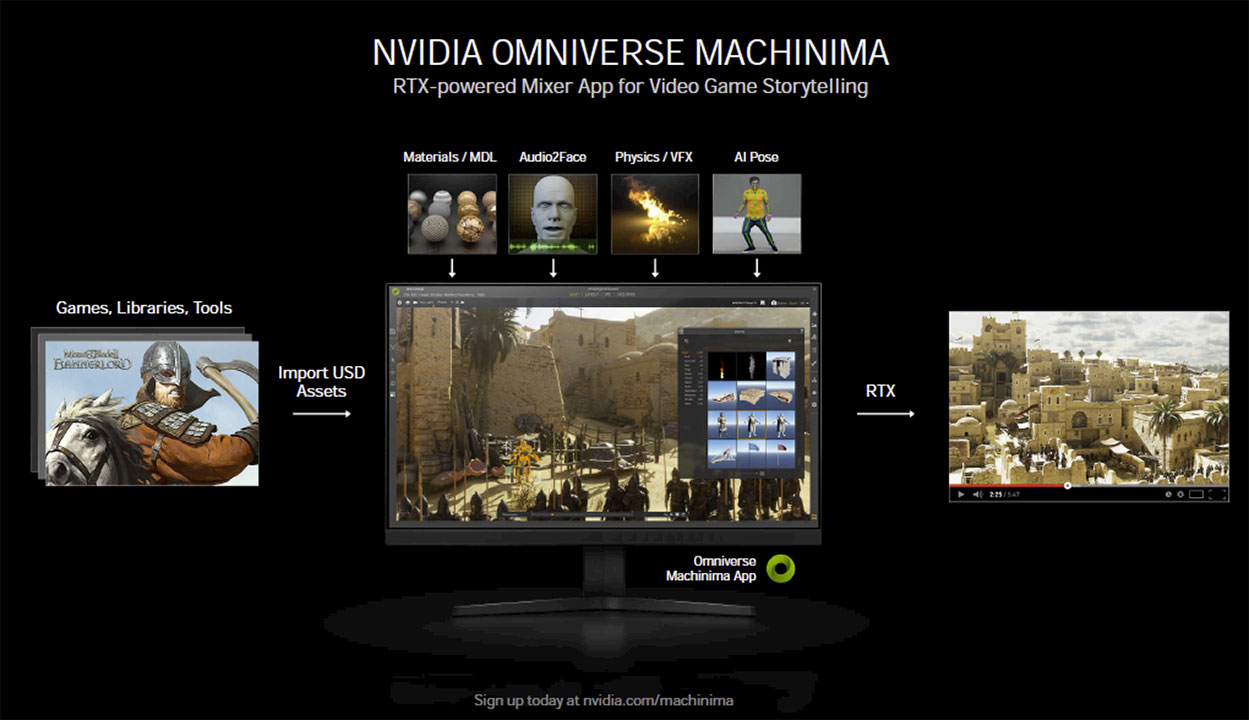

When NVIDIA introduced Ansel a few years ago, it spawned a new class of still art using in-game assets. What if you could make 3D animated movies using in-game assets? This concept is called machinima and already has a small, growing community of artists. NVIDIA wants to democratize and grow this ecosystem by introducing the new Omniverse Machinima software. When used with a supporting game, the software lets you make detailed 3D movies using all available game assets. Think making your own Star Trek fan fiction using STO assets.
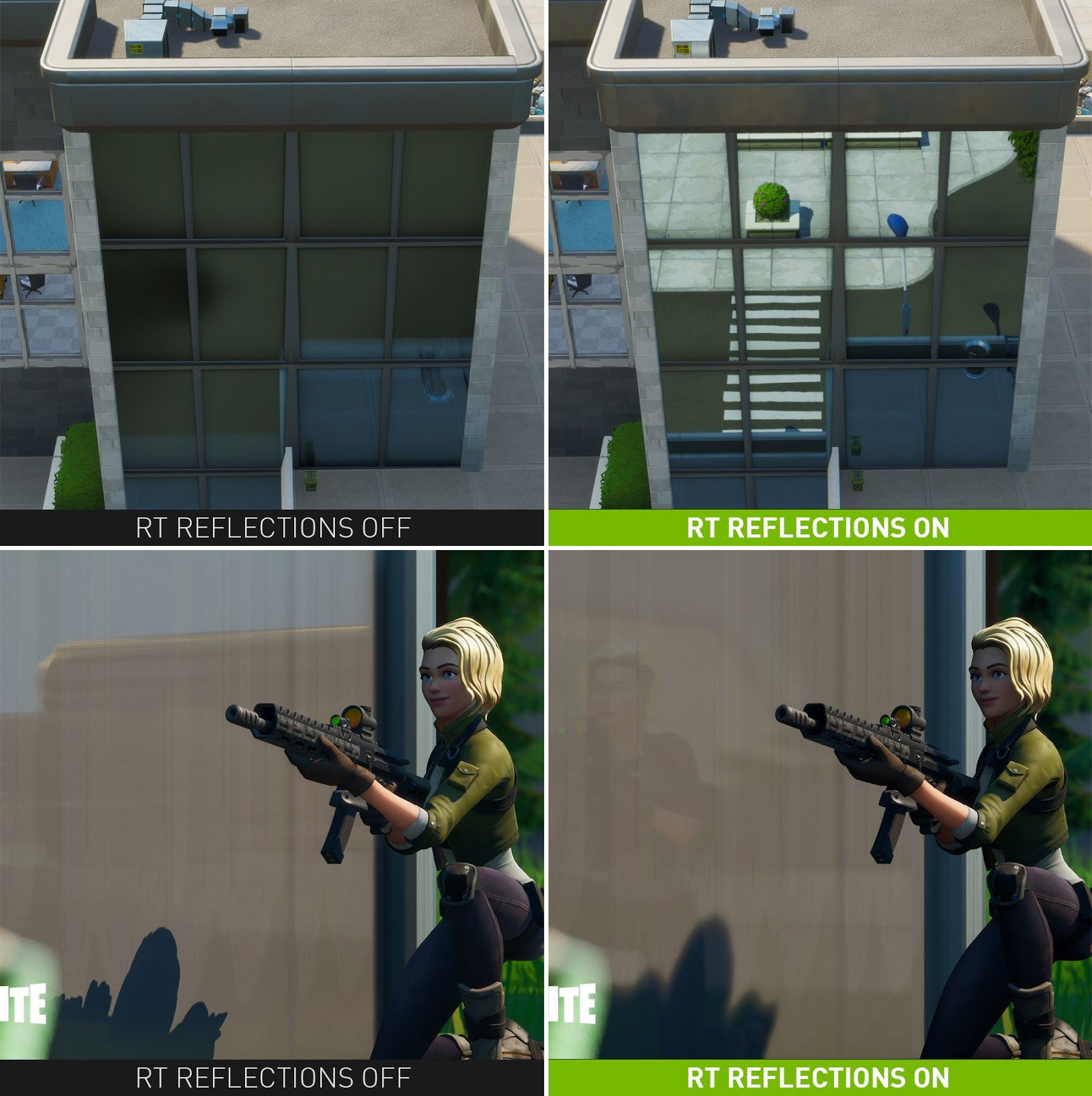

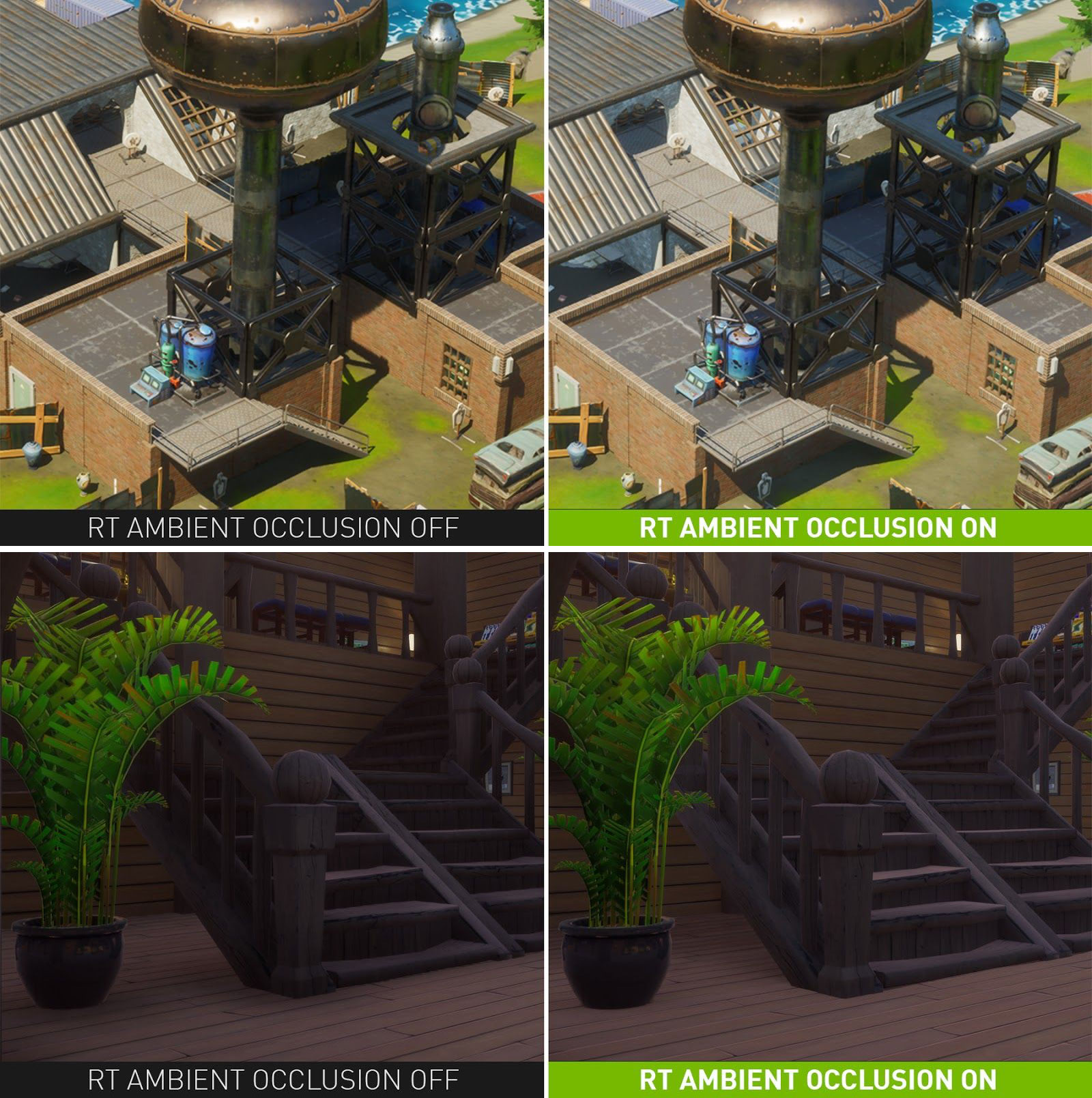
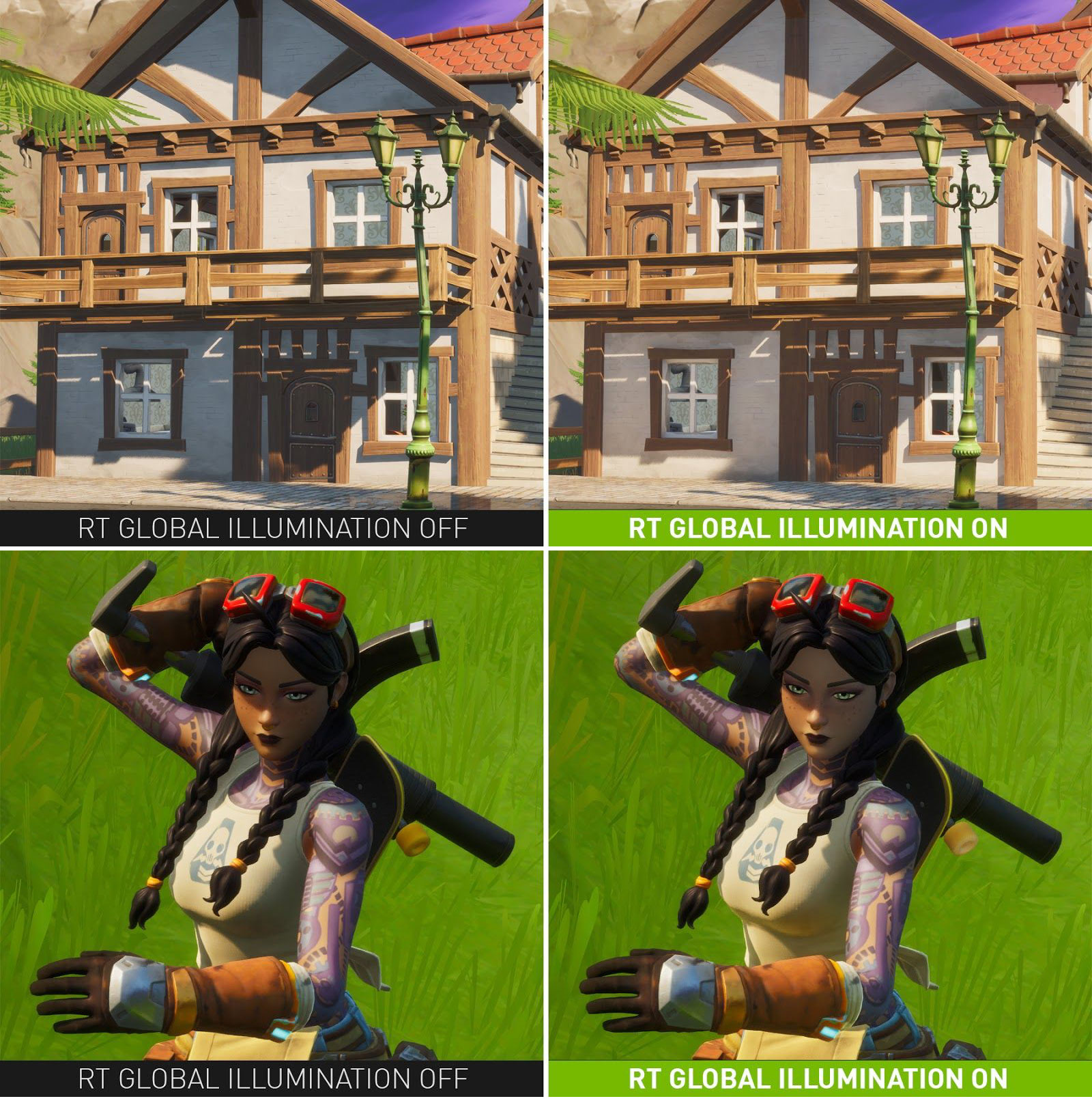
When you think about RTX, it's often AAA games that come to mind, and not competitive e-sports titles, as RTX inflicts a performance costs, and e-sports titles are designed to favor performance over eye candy. This is about to change with Fortnite going RTX-on. Fortnite uses almost the entire RTX feature set, including raytraced reflections, shadows, ambient occlusion, and global illumination. The game also implements DLSS, letting it render at a lower resolution, and using AI supersampling to restore details. Epic claims that DLSS at 4K looks better than even native 4K rendering.
Our Patreon Silver Supporters can read articles in single-page format.
May 7th, 2025 16:21 EDT
change timezone
Latest GPU Drivers
New Forum Posts
- RX 9000 series GPU Owners Club (720)
- How high of a ram frequency can i run on a Z690 with an 14700Kf processor? (15)
- Kindly help in Identifying GPU and Suitable bios (31)
- It's happening again, melting 12v high pwr connectors (1101)
- Request for advice [Big Build] (67)
- Forza Motorsport discussion thread (234)
- vccsa and vccio have another name AsRock ? (7)
- Asrock rx 5500 xt 8gb / I flashed BIOS, but I can't install drivers (3)
- Ventoy how to copy iso to the Ventoy drive? (5)
- Windows 11 PC takes ages to shut down. (8)
Popular Reviews
- Arctic Liquid Freezer III Pro 360 A-RGB Review
- Clair Obscur: Expedition 33 Performance Benchmark Review - 33 GPUs Tested
- ASUS Radeon RX 9070 XT TUF OC Review
- ASUS ROG Maximus Z890 Hero Review
- ASRock Radeon RX 9070 Steel Legend OC Review
- Upcoming Hardware Launches 2025 (Updated Apr 2025)
- Sapphire Radeon RX 9070 XT Nitro+ Review - Beating NVIDIA
- AMD Ryzen 7 9800X3D Review - The Best Gaming Processor
- SCYROX V6 Review
- Seasonic Vertex GX 850 W Review
Controversial News Posts
- AMD Radeon RX 9060 XT to Roll Out 8 GB GDDR6 Edition, Despite Rumors (142)
- NVIDIA Sends MSRP Numbers to Partners: GeForce RTX 5060 Ti 8 GB at $379, RTX 5060 Ti 16 GB at $429 (128)
- NVIDIA Launches GeForce RTX 5060 Series, Beginning with RTX 5060 Ti This Week (115)
- Microsoft Forces Automatic Windows 11 24H2 Update on Pro and Home PCs (90)
- Sony Increases the PS5 Pricing in EMEA and ANZ by Around 25 Percent (84)
- Parts of NVIDIA GeForce RTX 50 Series GPU PCB Reach Over 100°C: Report (78)
- Intel "Bartlett Lake-S" Gaming CPU is Possible, More Hints Appear for a 12 P-Core SKU (78)
- NVIDIA GeForce RTX 5060 Ti 8 GB Variant Benched by Chinese Reviewer, Lags Behind 16 GB Sibling in DLSS 4 Test Scenario (73)