 331
331
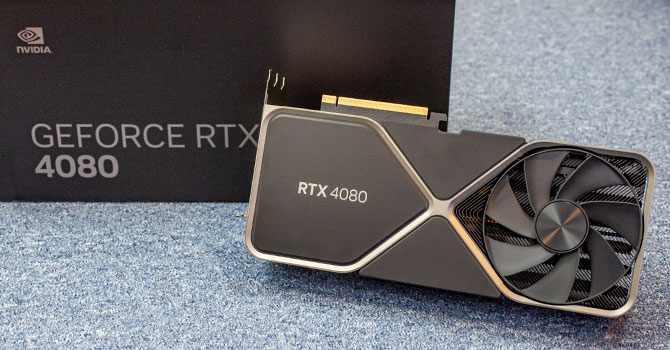
NVIDIA GeForce RTX 4080 Founders Edition Review - Energy-Efficient Beast
(331 Comments) »Introduction
NVIDIA GeForce RTX 4080 "Ada" is the the latest high-end graphics card from team-green after the sheer domination it brought to the high-end segment last month, with the RTX 4090. The new GeForce RTX 4080 SKU in this review succeeds the RTX 3080, which NVIDIA continued to maintain as its flagship product in the RTX 30-series till the end, treating everything higher as "halo" products. The RTX 4080 is designed with many of the same goals as the RTX 4090—to plow through games at maxed out settings at 4K, including ray tracing, but at a slightly more acceptable price point of $1,200, or 25% less. It is still designed to be faster than anything from the previous-generation.
NVIDIA had originally planned to fork the successor of the RTX 3080, the RTX 4080, into a sub-series of two SKUs, the RTX 4080 16 GB (covered in this review) and the now-cancelled RTX 4080 12 GB at $900—a price closer to the original RTX 3080 10 GB MSRP. This caused some controversy as the 12 GB variant was a vastly different product besides the memory size, and heaped bad press for NVIDIA in the social media. The RTX 4080 16 GB is hence now simply called the RTX 4080. We don't know for sure what NVIDIA will do with all those RTX 4080 12 GB that are already manufactured, probably re-brand them as some other SKU, we'll have to see.
With the RTX 40-series "Ada" generation, NVIDIA achieved a minor course-correction in the way the RTX 4080 is created. Since it is bound to sell in greater volumes than the RTX 4090, the company isn't carving the SKU out by basing it on the same large AD102 silicon and disabling a ton of CUDA cores. There was a large gap in the CUDA core counts between the previous-generation GA104 and GA102, which allowed AMD to slip in competitive products such as the RX 6800, which couldn't be beaten by any GA104-based SKU, including the RTX 3070 Ti. Therefore, NVIDIA developed a new in-between silicon between the two, to better optimize manufacturing costs, the AD103. There is such a silicon even in past generations, such as GA103, but those were confined to the mobile platforms.
The new 5 nm AD103 silicon only has two-thirds the die area of the AD102, which amounts to great manufacturing cost savings. Its memory interface is slashed by a third, too, with a 256-bit GDDR6X memory interface. NVIDIA has increased the memory size generation-over-generation, to 16 GB (up from 12 GB or 10 GB of the RTX 3080), however, the memory bus is narrowed, and while the memory speed is only marginally higher at 22.4 Gbps (versus 19.5 Gbps), the overall memory bandwidth is lesser, at 716 GB/s, compared to 760 GB/s of the RTX 3080 10 GB. This shortfall in memory bandwidth is claimed to be compensated for with architectural improvements, such as larger on-die caches.
The GeForce RTX 4080 is endowed with 9,728 CUDA cores across 76 streaming multiprocessors (SMs) out of the 80 physically present on the silicon. it gets 76 RT cores, 304 Tensor cores, 304 TMUs, and 112 ROPs. NVIDIA has generationally increased GPU clock speeds, and the RTX 4080 ticks at 2.25 GHz, with a memory speed of 22.5 Gbps (GDDR6X effective). The typical power of the card is 320 W, nearly 25% lower than that of the RTX 4090, and many of the board partners appear to be using cooling solutions they originally designed for the RTX 4090, meaning the custom-design RTX 4080 cards should run quieter.
NVIDIA GeForce RTX 4080 Founders Edition is the company's take on a premium custom-design card of its own. This isn't a "reference design" by any stretch, but an attempt by NVIDIA engineers to establish a high benchmark for product design for its board partners to beat with their custom-designs. The RTX 4080 Founders Edition (FE) card looks practically identical in shape and dimensions to that of the RTX 4090 FE, which means the GPU will benefit from a cooling solution that was designed to deal with a more power-hungry GPU. The most interesting aspect of the FE package is the included adapter that converts 8-pin PCIe into 16-pin 12VHPWR—it only has three 8-pin connectors, compared to four on the one NVIDIA includes with the RTX 4090 cards. The adapter is keyed for 450 W power delivery, identical to the one included with the RTX 3090 Ti.
| Price | Cores | ROPs | Core Clock | Boost Clock | Memory Clock | GPU | Transistors | Memory | |
|---|---|---|---|---|---|---|---|---|---|
| RTX 2080 | $380 | 2944 | 64 | 1515 MHz | 1710 MHz | 1750 MHz | TU104 | 13600M | 8 GB, GDDR6, 256-bit |
| RTX 3060 Ti | $410 | 4864 | 80 | 1410 MHz | 1665 MHz | 1750 MHz | GA104 | 17400M | 8 GB, GDDR6, 256-bit |
| RX 6700 XT | $360 | 2560 | 64 | 2424 MHz | 2581 MHz | 2000 MHz | Navi 22 | 17200M | 12 GB, GDDR6, 192-bit |
| RX 6750 XT | $470 | 2560 | 64 | 2495 MHz | 2600 MHz | 2250 MHz | Navi 22 | 17200M | 12 GB, GDDR6, 192-bit |
| RTX 2080 Ti | $600 | 4352 | 88 | 1350 MHz | 1545 MHz | 1750 MHz | TU102 | 18600M | 11 GB, GDDR6, 352-bit |
| RTX 3070 | $500 | 5888 | 96 | 1500 MHz | 1725 MHz | 1750 MHz | GA104 | 17400M | 8 GB, GDDR6, 256-bit |
| RTX 3070 Ti | $600 | 6144 | 96 | 1575 MHz | 1770 MHz | 1188 MHz | GA104 | 17400M | 8 GB, GDDR6X, 256-bit |
| RX 6800 | $580 | 3840 | 96 | 1815 MHz | 2105 MHz | 2000 MHz | Navi 21 | 26800M | 16 GB, GDDR6, 256-bit |
| RX 6800 XT | $530 | 4608 | 128 | 2015 MHz | 2250 MHz | 2000 MHz | Navi 21 | 26800M | 16 GB, GDDR6, 256-bit |
| RTX 3080 | $660 | 8704 | 96 | 1440 MHz | 1710 MHz | 1188 MHz | GA102 | 28000M | 10 GB, GDDR6X, 320-bit |
| RTX 3080 Ti | $950 | 10240 | 112 | 1365 MHz | 1665 MHz | 1188 MHz | GA102 | 28000M | 12 GB, GDDR6X, 384-bit |
| RX 6900 XT | $650 | 5120 | 128 | 2015 MHz | 2250 MHz | 2000 MHz | Navi 21 | 26800M | 16 GB, GDDR6, 256-bit |
| RX 6950 XT | $800 | 5120 | 128 | 2100 MHz | 2310 MHz | 2250 MHz | Navi 21 | 26800M | 16 GB, GDDR6, 256-bit |
| RTX 3090 | $900 | 10496 | 112 | 1395 MHz | 1695 MHz | 1219 MHz | GA102 | 28000M | 24 GB, GDDR6X, 384-bit |
| RX 7900 XT | $900 | 5376 | 192 | 2000 MHz | 2400 MHz | 2500 MHz | Navi 31 | 58000M | 20 GB, GDDR6, 320-bit |
| RTX 3090 Ti | $1400 | 10752 | 112 | 1560 MHz | 1950 MHz | 1313 MHz | GA102 | 28000M | 24 GB, GDDR6X, 384-bit |
| RX 7900 XTX | $1000 | 6144 | 192 | 2300 MHz | 2505 MHz | 2500 MHz | Navi 31 | 58000M | 24 GB, GDDR6, 384-bit |
| RTX 4080 | $1200 | 9728 | 112 | 2205 MHz | 2505 MHz | 1400 MHz | AD103 | 45900M | 16 GB, GDDR6X, 256-bit |
| RTX 4090 | $2400 | 16384 | 176 | 2235 MHz | 2520 MHz | 1313 MHz | AD102 | 76300M | 24 GB, GDDR6X, 384-bit |
Architecture
The Ada graphics architecture heralds the third generation of the NVIDIA RTX technology, an effort toward increasing the realism of game visuals by leveraging real-time ray tracing, without the enormous amount of compute power required to draw purely ray-traced 3D graphics. This is done by blending conventional raster graphics with ray traced elements such as reflections, lighting, and global illumination, to name a few. The 3rd generation of RTX heralds the new higher IPC "Ada" CUDA core, 3rd generation RT core, 4th generation Tensor core, and the new Optical Flow Processor, a component that plays a key role in generating new frames without involving the GPU's main graphics rendering pipeline.
The GeForce Ada graphics architecture driving the RTX 4080 leverages the TSMC 5 nm EUV foundry process to increase transistor counts. At the heart of the RTX 4080 is the new AD103 silicon, which has a reasonably large transistor count of 45.9 billion, which is still nearly 60% higher than that of the previous-generation flagship GA102. The GPU features a PCI-Express 4.0 x16 host interface, and a 256-bit wide GDDR6X memory bus, which on the RTX 4080 wires out to 16 GB of memory. With NVIDIA cancelling the 12 GB variant, this is the only RTX 4080 there is, for now. The Optical Flow Accelerator (OFA) is an independent top-level component. The chip features two NVENC and one NVDEC units in the GeForce RTX 40-series.
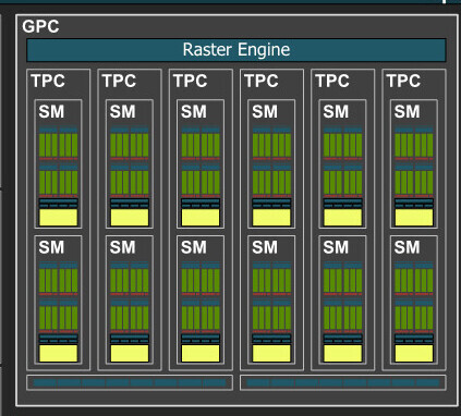
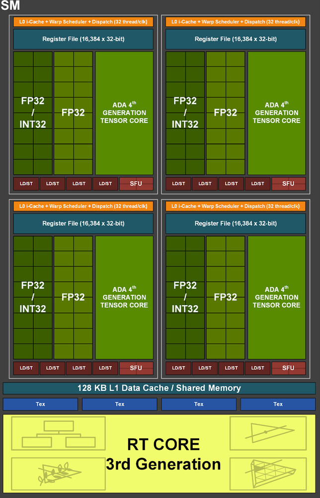
The essential component hierarchy is similar to past generations of NVIDIA GPUs. The AD103 silicon features 7 Graphics Processing Clusters (GPCs), each of these has all the SIMD and graphics rendering machinery, and is a small GPU in its own right. Each GPC shares a raster engine (geometry processing components) and two ROP partitions (each with eight ROP units). The GPC of the AD102 contains six Texture Processing Clusters (TPCs), the main number-crunching machinery. Each of these has two Streaming Multiprocessors (SM), and a Polymorph unit. Each SM contains 128 CUDA cores across four partitions. Half of these CUDA cores are pure-FP32; while the other half is capable of FP32 or INT32. The SM retains concurrent FP32+INT32 math processing capability. The SM also contains a 3rd generation RT core, four 4th generation Tensor cores, some cache memory, and four TMUs. There are 12 SM per GPC, so 1,536 CUDA cores, 48 Tensor cores, and 12 RT cores; per GPC. There are seven such GPCs, which add up to 10,240 CUDA cores, 320 TMUs, 320 Tensor Cores, 80 RT cores. Each GPC contributes 16 ROPs, so there are 112 ROPs on the silicon. NVIDIA carved the RTX 4080 out of the AD103 by disabling four SMs.
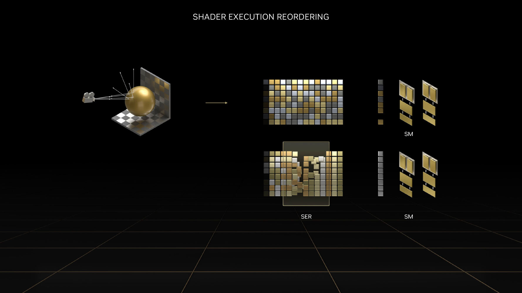
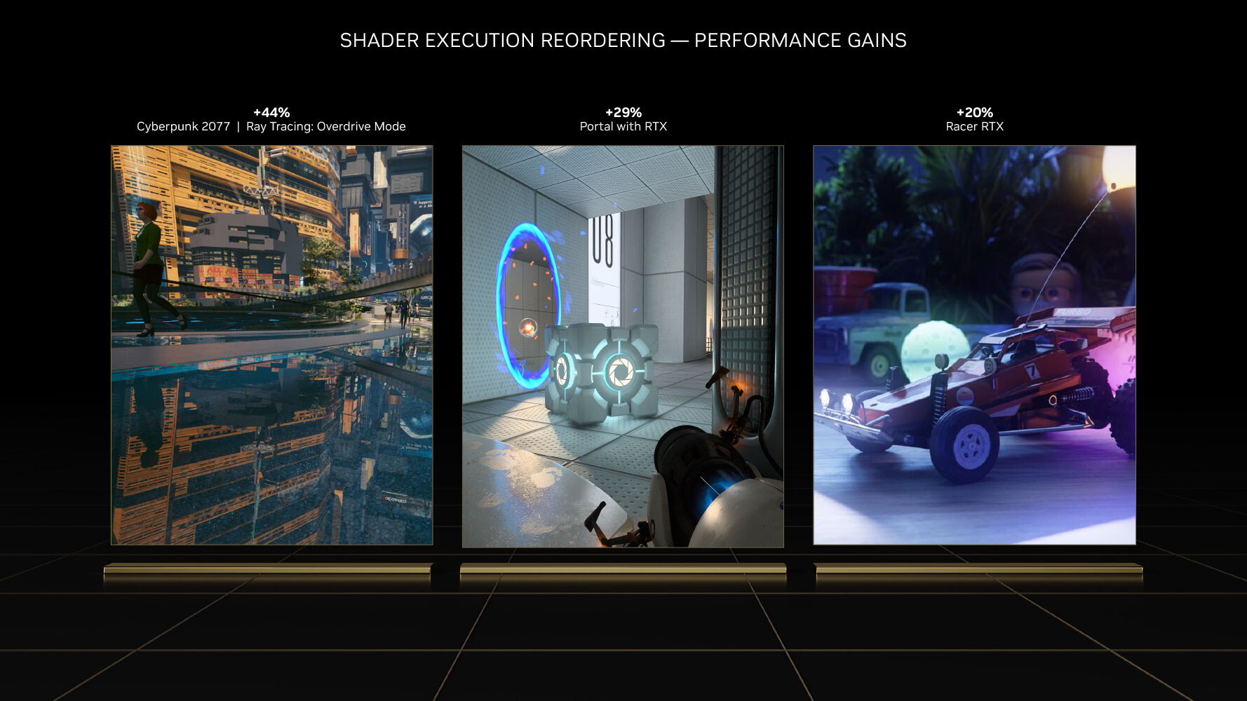
The 3rd generation RT core accelerates the most math-intensive aspects of real-time ray tracing, including BVH traversal. Displaced micro-mesh engine is a revolutionary feature introduced with the new 3rd generation RT core. Just as mesh shaders and tessellation have had a profound impact on improving performance with complex raster geometry, allowing game developers to significantly increase geometric complexity; DMMs is a method to reduce the complexity of the bounding-volume hierarchy (BVH) data-structure, which is used to determine where a ray hits geometry. Previously, the BVH had to capture even the smallest details to properly determine the intersection point. Ada's ray tracing architecture also receives a major performance uplift from Shader Execution Reordering (SER), a software-defined feature that requires awareness from game-engines, to help the GPU reorganize and optimize worker threads associated with ray tracing.

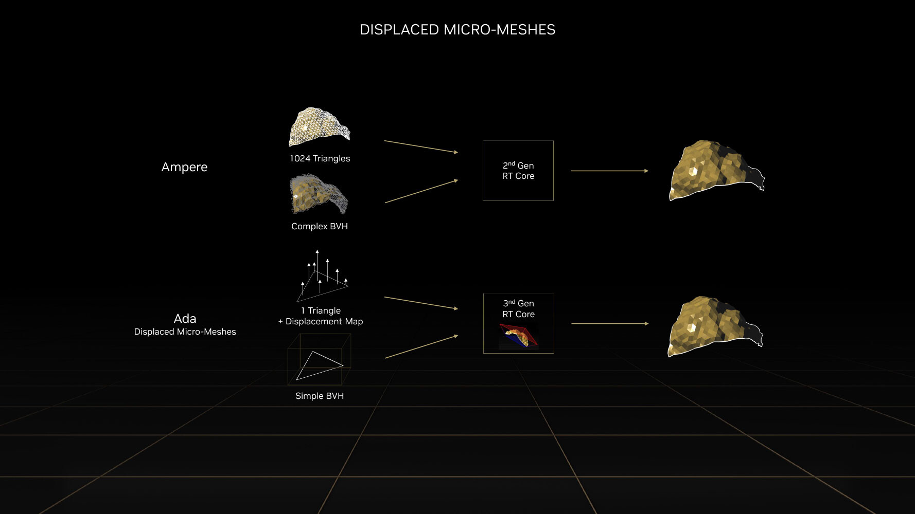
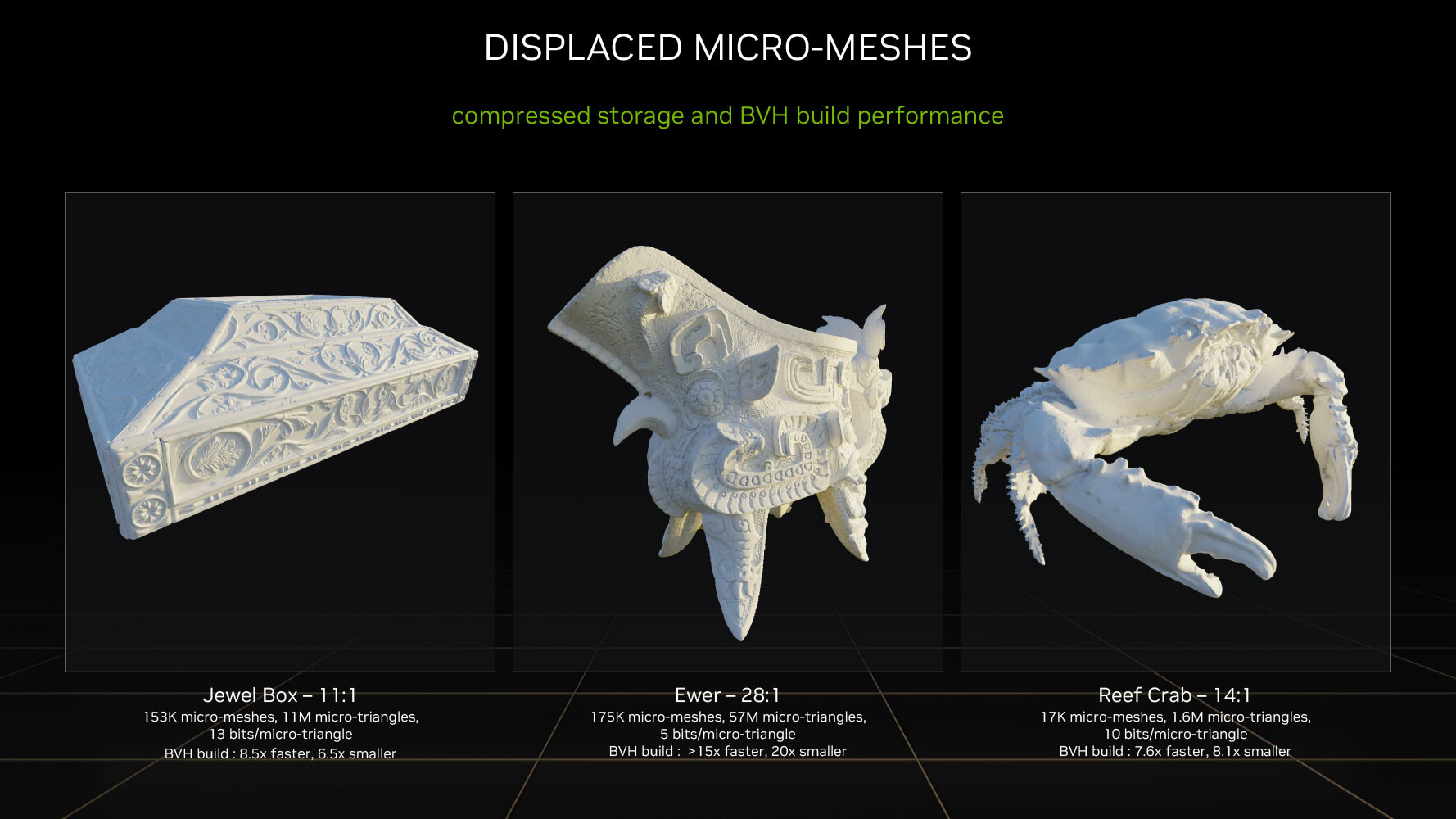
The BVH now needn't have data for every single triangle on an object, but can represent objects with complex geometry as a coarse mesh of base triangles, which greatly simplifies the BVH data structure. A simpler BVH means less memory consumed and helps to greatly reduce ray tracing CPU load, because the CPU only has to generate a smaller structure. With older "Ampere" and "Turing" RT cores, each triangle on an object had to be sampled at high overhead, so the RT core could precisely calculate ray intersection for each triangle. With Ada, the simpler BVH, plus the displacement maps can be sent to the RT core, which is now able to figure out the exact hit point on its own. NVIDIA has seen 11:1 to 28:1 compression in total triangle counts. This reduces BVH compile times by 7.6x to over 15x, in comparison to the older RT core; and reducing its storage footprint by anywhere between 6.5 to 20 times. DMMs could reduce disk- and memory bandwidth utilization, utilization of the PCIe bus, as well as reduce CPU utilization. NVIDIA worked with Simplygon and Adobe to add DMM support for their tool chains.

Opacity Micro Meshes (OMM) is a new feature introduced with Ada to improve rasterization performance, particularly with objects that have alpha (transparency data). Most low-priority objects in a 3D scene, such as leaves on a tree, are essentially rectangles with textures on the leaves where the transparency (alpha) creates the shape of the leaf. RT cores have a hard time intersecting rays with such objects, because they're not really in the shape that they appear (they're really just rectangles with textures that give you the illusion of shape). Previous-generation RT cores had to have multiple interactions with the rendering stage to figure out the shape of a transparent object, because they couldn't test for alpha by themselves.


This has been solved by using OMMs. Just as DMMs simplify geometry by creating meshes of micro-triangles; OMMs create meshes of rectangular textures that align with parts of the texture that aren't alpha, so the RT core has a better understanding of the geometry of the object, and can correctly calculate ray intersections. This has a significant performance impact on shading performance in non-RT applications, too. Practical applications of OMMs aren't just low-priority objects such as vegetation, but also smoke-sprites and localized fog. Traditionally there was a lot of overdraw for such effects, because they layered multiple textures on top of each other, that all had to be fully processed by the shaders. Now only the non-opaque pixels get executed—OMMs provide a 30 percent speedup with graphics buffer fill-rates, and a 10 percent impact on frame-rates.
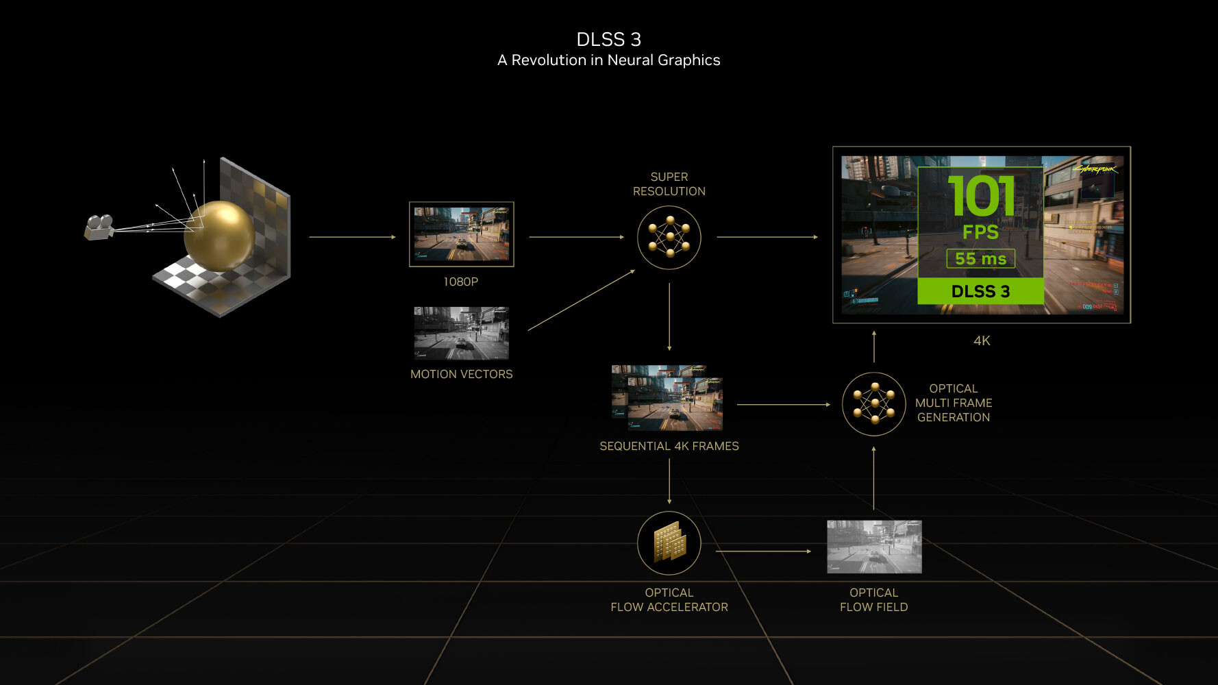
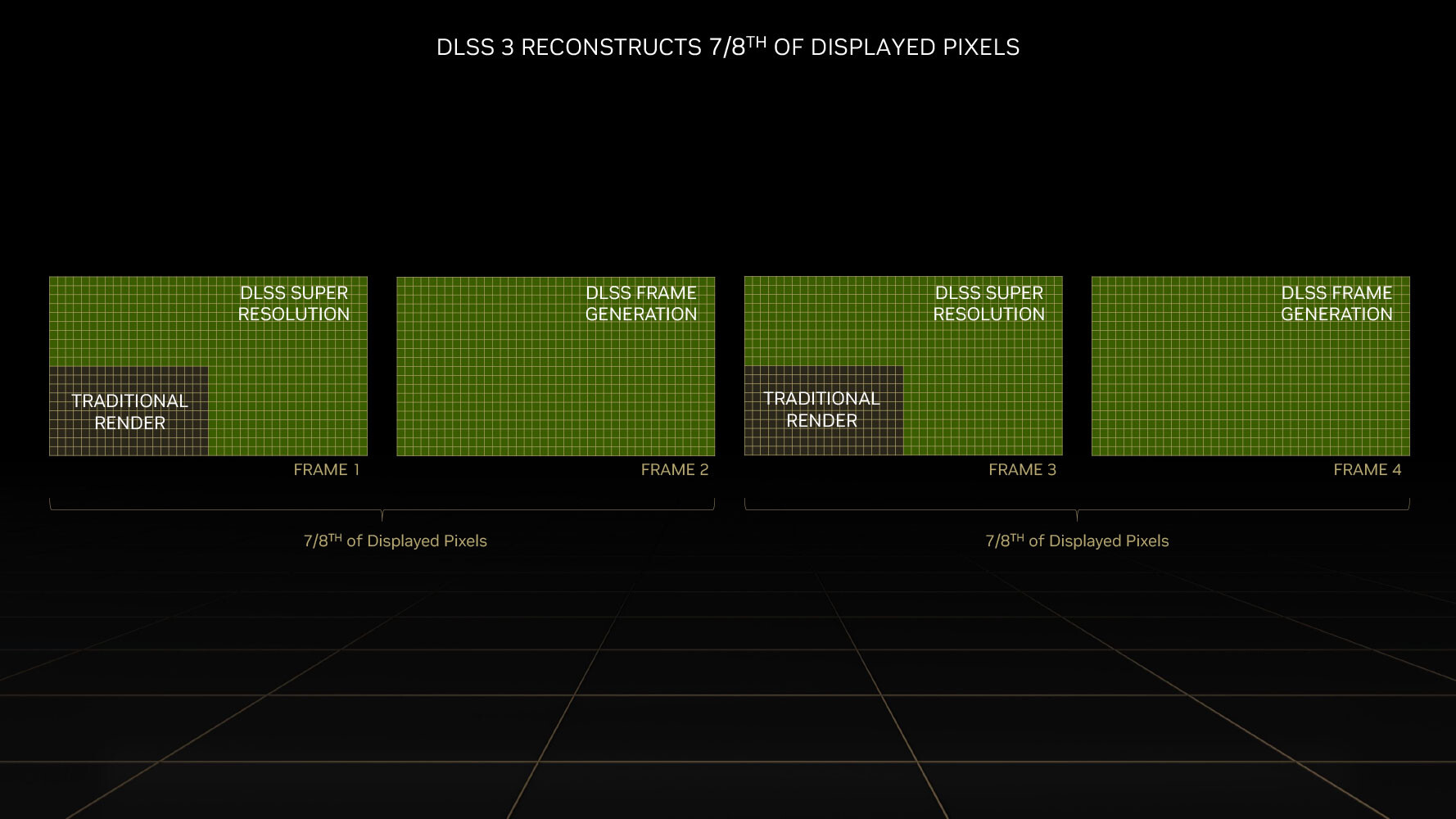
DLSS 3 introduces a revolutionary new feature that promises a doubling in frame-rate at comparable quality, it's called AI frame-generation. While it has all the features of DLSS 2 and its AI super-resolution (scaling up a lower-resolution frame to native resolution with minimal quality loss); DLSS 3 can generate entire frames simply using AI, without involving the graphics rendering pipeline. Later in the article, we will show you DLSS 3 in action.
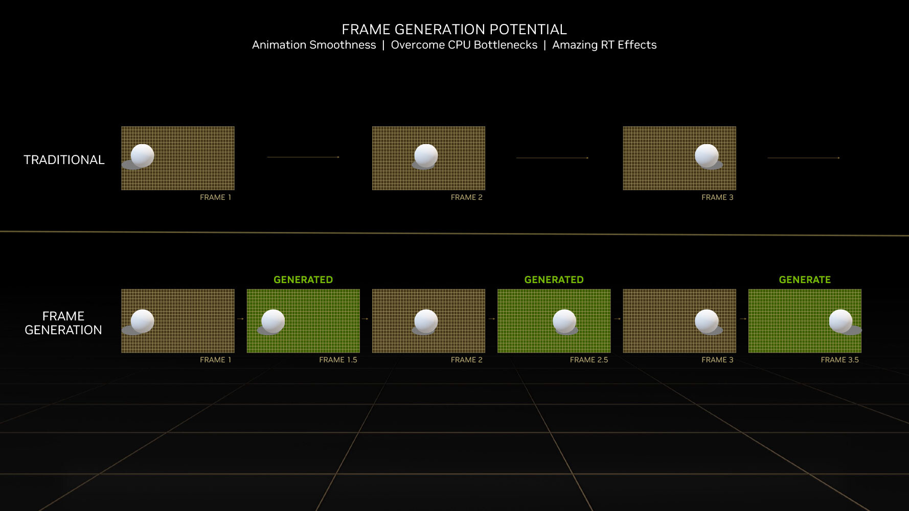

Every alternating frame with DLSS 3 is hence AI-generated, without being a replica of the previous rendered frame. This is possible only on the Ada graphics architecture, because of a hardware component called the optical flow accelerator (OFA), which assists in predicting what the next frame could look like, by creating what NVIDIA calls an optical flow-field. OFA ensures that the DLSS 3 algorithm isn't confused by static objects in a rapidly-changing 3D scene (such as a race sim). The process heavily relies on the performance uplift introduced by the FP8 math format of the 4th generation Tensor core. A third key ingredient of DLSS 3 is Reflex. By reducing the rendering queue to zero, Reflex plays a vital role in ensuring that frame-times with DLSS 3 are at an acceptable level, and a render-queue doesn't confuse the upscaler. A combination of OFA and the 4th Gen Tensor core is why the Ada architecture is required to use DLSS 3, and why it won't work on older architectures.
Packaging

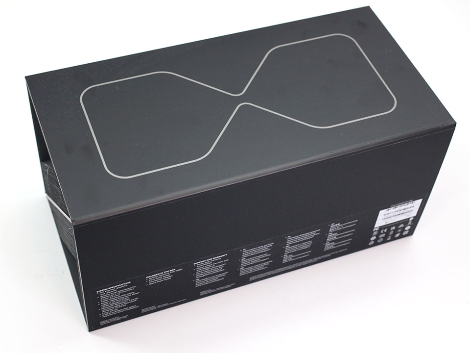
RTX 4080 Founders Edition comes in a huge flip-open package.
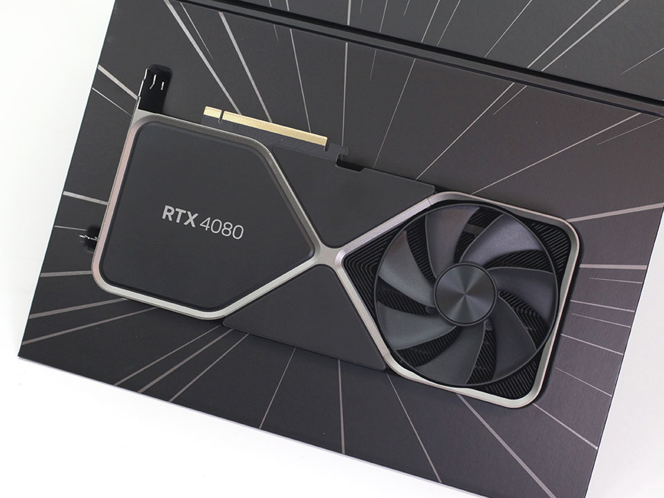
The card sits neatly in the center, underneath the card you'll find documentation and the PCIe adapter cable.
The Card
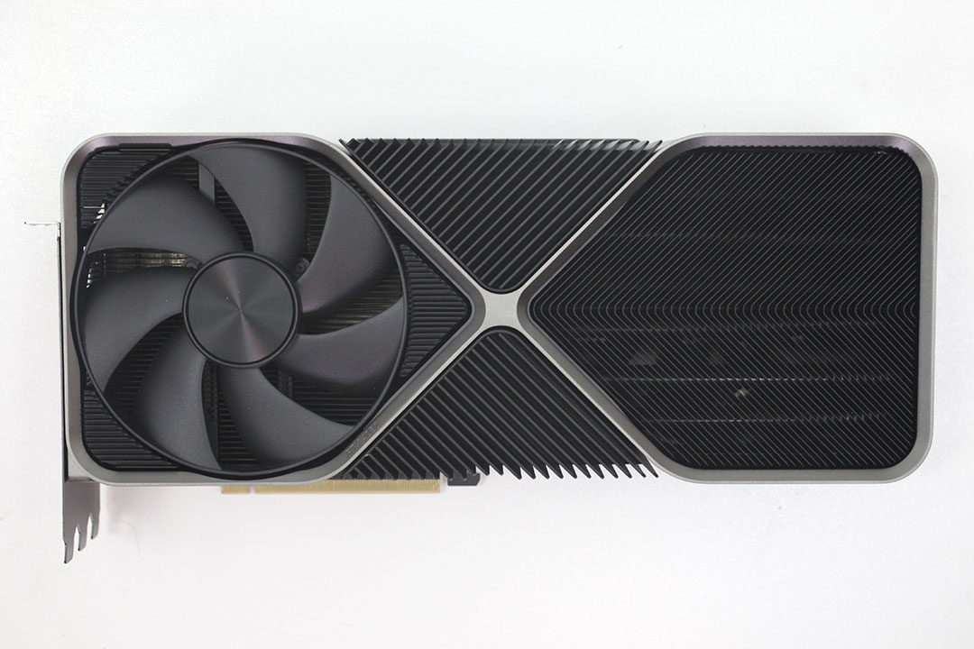
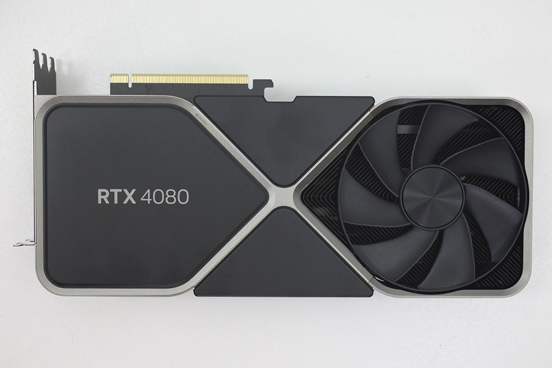
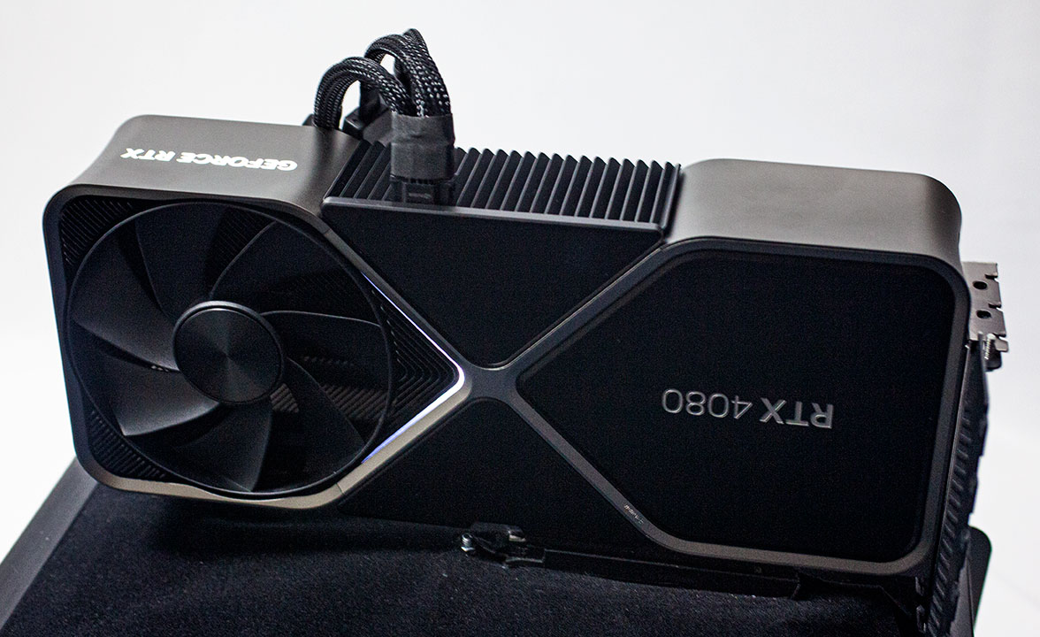
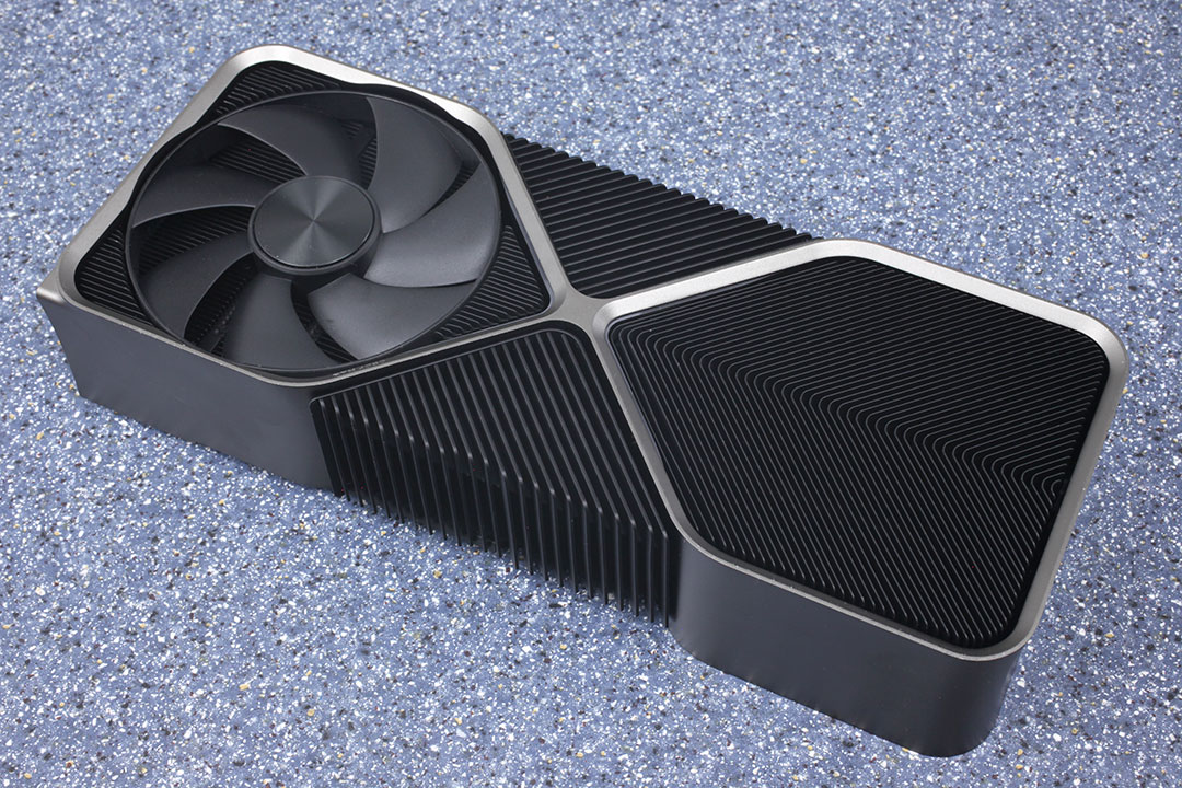
NVIDIA's Founders Edition looks stunning—it could be an Apple product. Compared to the GeForce 30 Series, NVIDIA has made small improvements to the design language, making it an even cleaner design than before. Visually the GeForce RTX 4080 Founders Edition looks identical to the RTX 4090 Founders Edition, both cards use the same cooler. The PCB is also very similar, although there are small differences. As with Ampere, the card is designed for airflow to go through the card—that's why there's two fans. One sucks in cool air from the bottom, is pushed through the card and then blown out towards the case top on the other side.
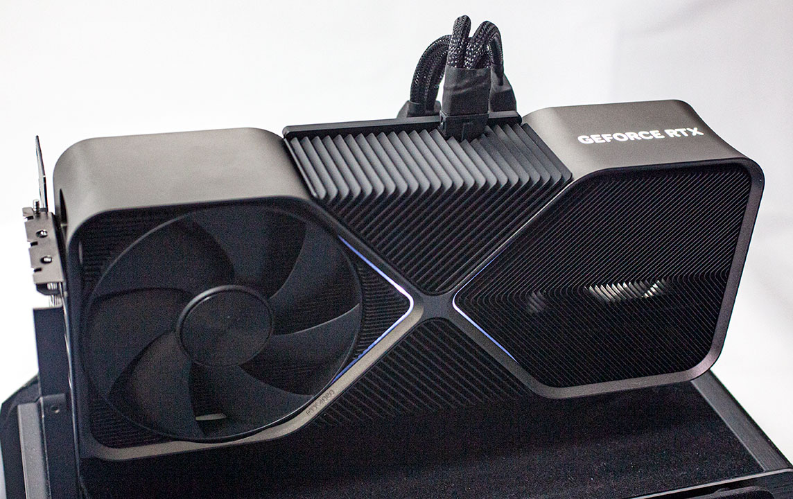
NVIDIA includes an illuminated "GeForce RTX" logo and three illumination zones near the card center, between the two fans.
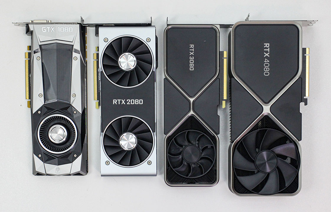
From left to right: GTX 1080, RTX 2080, RTX 3080, RTX 4080
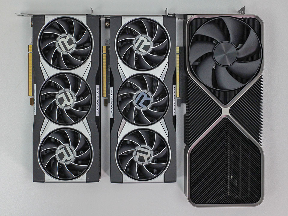

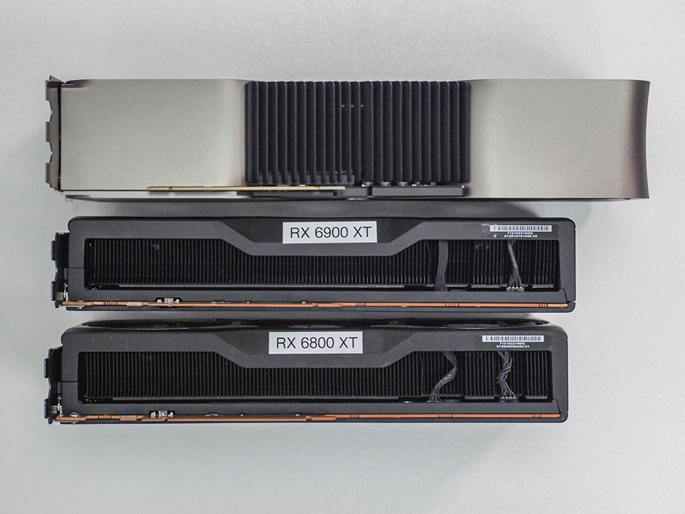
Compared against AMD's recent offerings it becomes clear how large this card really is.
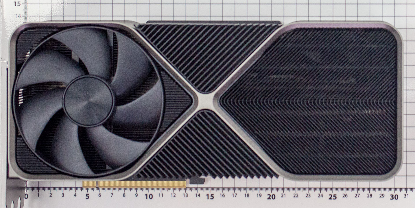

Dimensions of the card are 31.0 x 14.0 cm, and it weighs 2131 g.
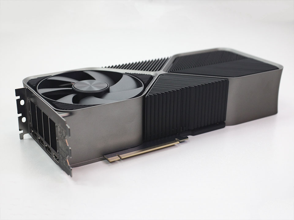

Installation requires three slots in your system.

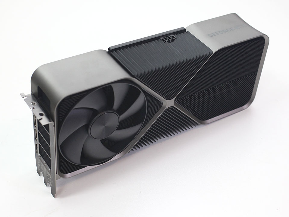
Display connectivity includes three standard DisplayPort 1.4a ports and one HDMI 2.1a (same as Ampere).
NVIDIA introduces the concept of dual NVDEC and NVENC Codecs with the Ada architecture. This means there are now two independent sets of hardware-accelerators; so you can encode and decode two streams of video in parallel, or one stream at double the FPS rate. The new 8th Gen NVENC now accelerates AV1 encoding, besides HEVC. You also get an "optical flow accelerator" unit that is able to calculate intermediate frames for videos, to smooth playback. The same hardware unit is used for frame generation in DLSS 3.


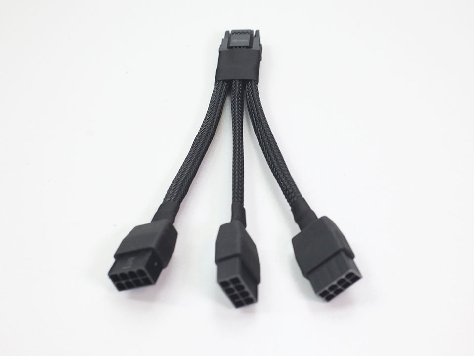
The card uses the new 12+4 pin ATX 12VHPWR connector, which is rated for up to 450 W of power draw. An adapter cable from 3x PCIe 8-pin is included. Of course the 4x 8-pin to 16-pin adapter cables from RTX 4090 will also work with the RTX 4080.


The tail end of the card has a small lid that covers the mounting holes for a support rail, used in certain workstation form-factors such as the x86 Mac Pro.
Teardown
Taking the RTX 4080 Founders Edition apart isn't much different to previous Founders Edition cards and can be done in a few minutes, if you know what you're doing.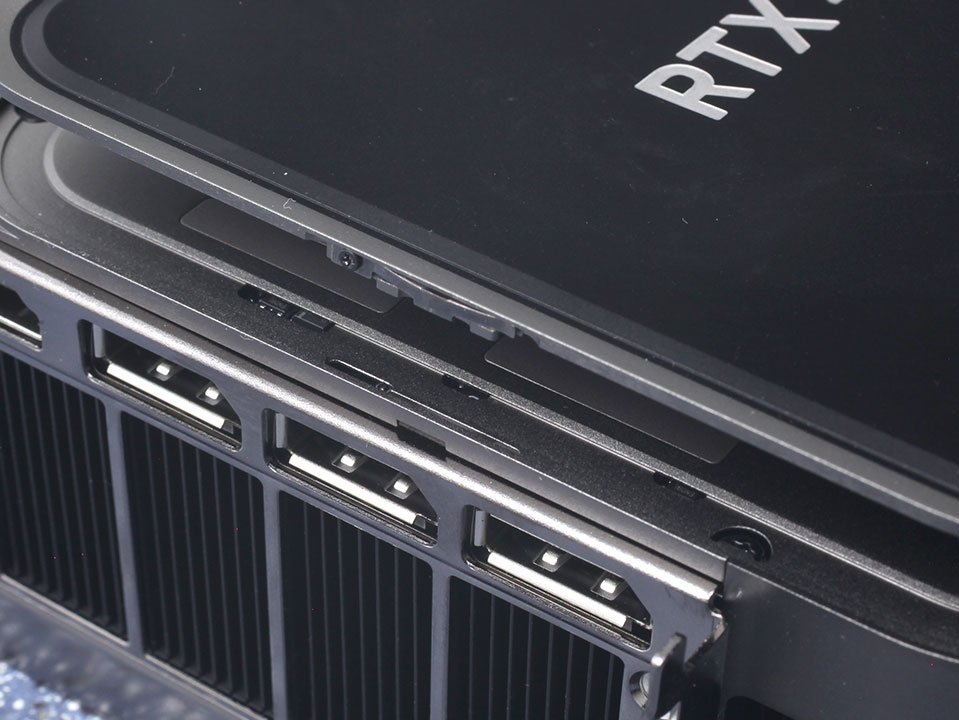

First pop off the top cover with the "RTX 4080" text on it. To do that carefully lift it up from the PCIe slot cover side, it's attached magnetically, but there's also a small metal tab that you might have to press inwards if the cover doesn't lift off immediately. Remove the screws that become accessible, and then take off the backplate.
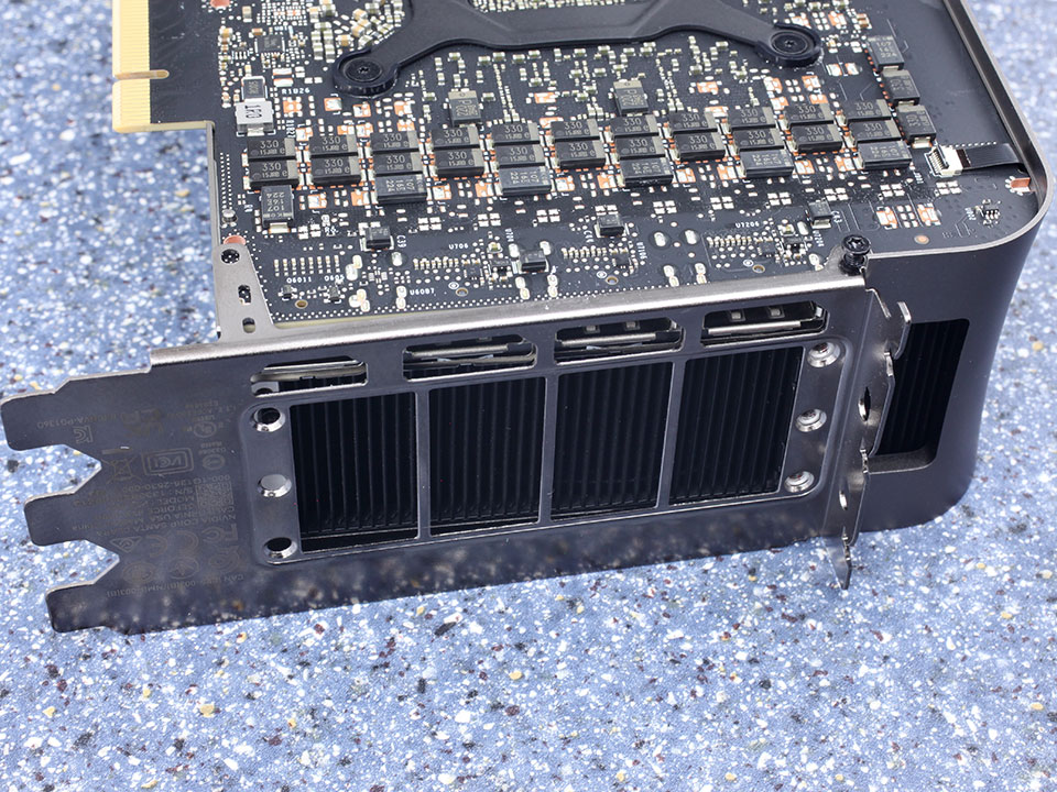
Now you can remove the six Torx screws on the slot cover, and one more screw near the top right in the second picture, that holds the slot cover in place.

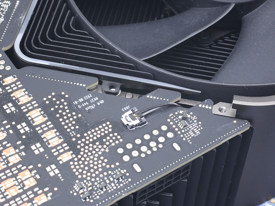

We've seen these before, flip up the flat-ribbon connector carefully (I prefer to use my fingers rather than pliers), and carefully pull out the flat-ribbon cable. The other connector with the silvery cover requires you to push the cover sideways, and then you can lift the black plastic connector upwards. More info here.
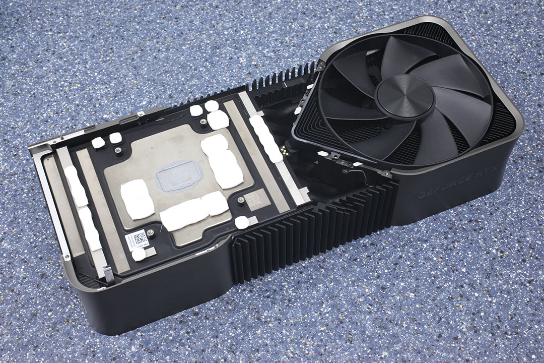
The main heatsink is a beastly cooling solution. It provides cooling for the GPU, memory chips and VRM circuitry. A large vapor-chamber sucks up heat from the GPU and moves it to the heatsink using heatpipes.
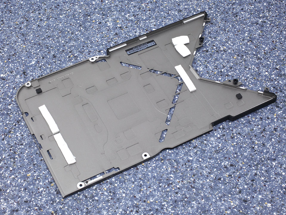

This "backplate" is designed so that air can flow through it, that's why it doesn't cover the whole card.
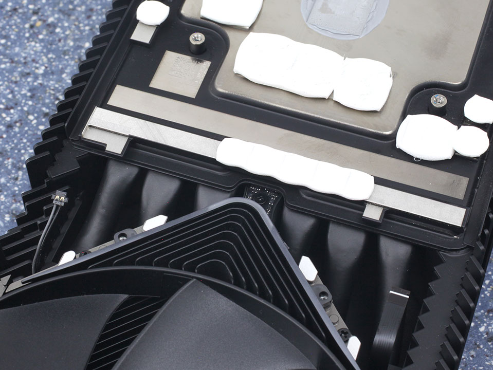
NVIDIA uses six fat heatpipes and a vapor-chamber plate to move heat away from the GPU quickly.
High-resolution PCB Pictures
These pictures are for the convenience of volt modders and people who would like to see all the finer details on the PCB. Feel free to link back to us and use these in your articles, videos or forum posts.

High-resolution versions are also available (front, back).
Circuit Board (PCB) Analysis
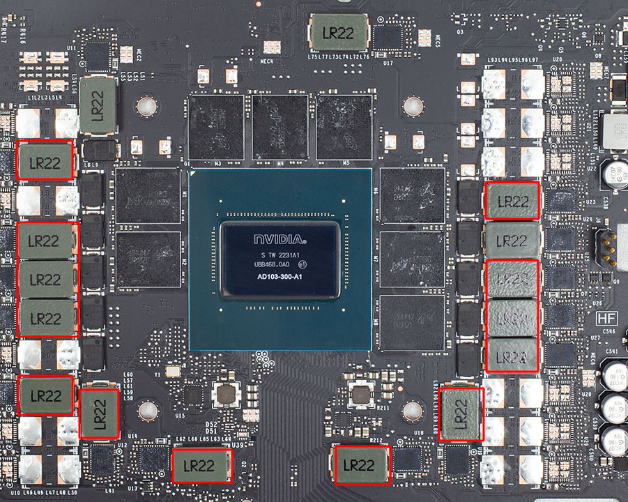

GPU voltage is a 13-phase design, managed by a Monolithic Power Systems MP2891 controller, which also handles memory voltage.
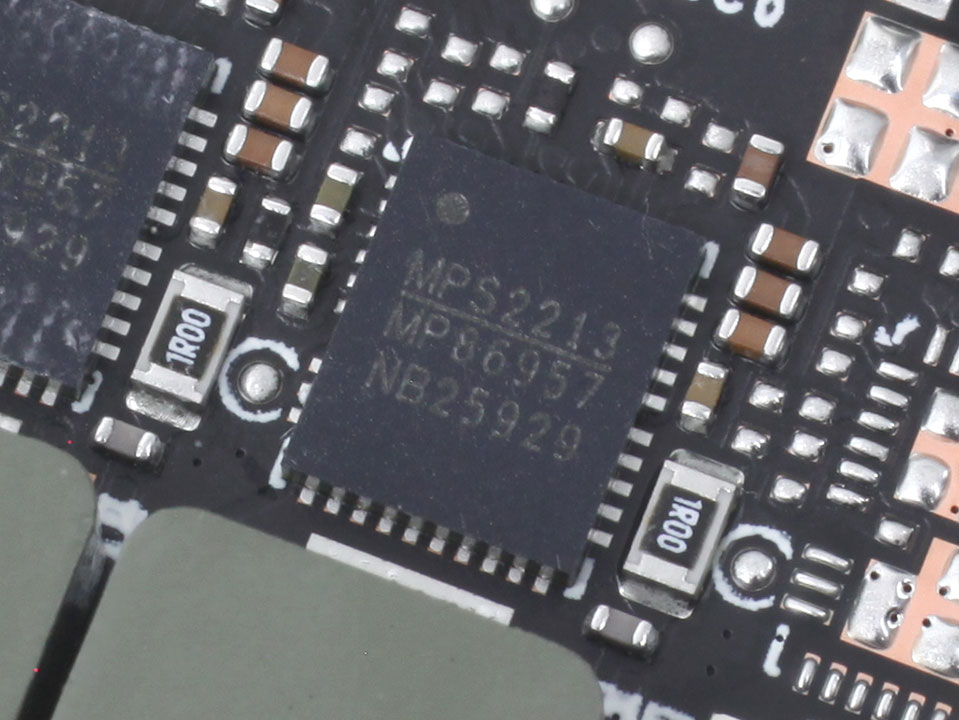
Monolithic MP86957 DrMOS components are used for GPU voltage; they are rated for 70 A of current each.

Memory voltage is a three-phase design, managed by the same MP2891 that's used for GPU voltage.
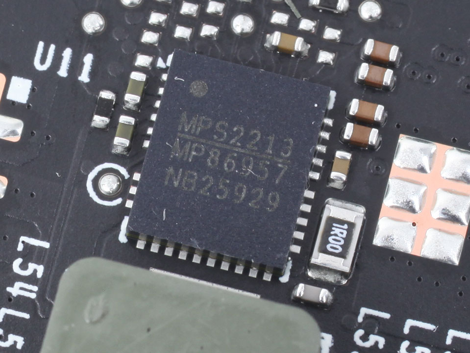
For memory, Monolithic MP86957 DrMOS with a 70 A rating are used again.

The GDDR6X memory chips are made by Micron and carry the model number D8BZF, which decodes to MT61K512M32KPA-24. They are specified to run at 1500 MHz (24 Gbps effective).
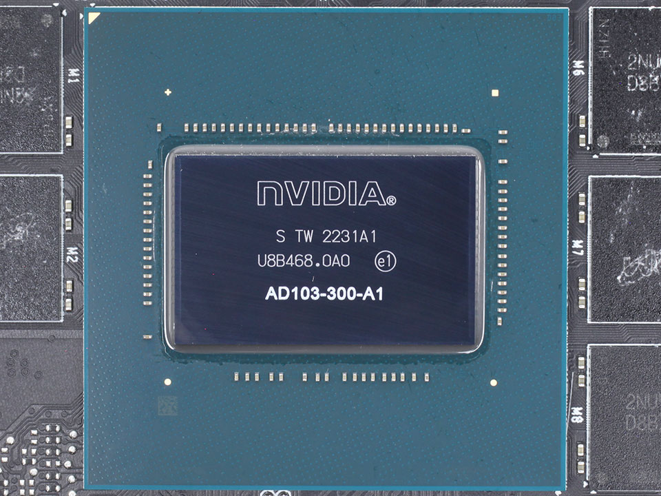
NVIDIA's AD103 graphics processor is the company's second Ada Lovelace GPU. It is built using a 5 nanometer process at TSMC Taiwan, with a transistor count of 45.9 billion and a die size of 379 mm².
Our Patreon Silver Supporters can read articles in single-page format.
May 5th, 2025 11:52 EDT
change timezone
Latest GPU Drivers
New Forum Posts
- What phone you use as your daily driver? And, a discussion of them. (1671)
- WD Black or Gold for Gaming (10TB) (36)
- RX 9000 series GPU Owners Club (648)
- Do you prefer factory overclocked GPUs? (66)
- Post Your TIMESPY, PCMARK10 & FIRESTRIKE SCORES! (2019) (295)
- [AV1, AV2, AV3 codecs...] Have they given up on the AOMedia project? (22)
- Question about photos (4)
- Can't connecte my xbox controller to my pc (ugreen bt adapter) (7)
- Corsair Type 3 vs 4 cables [SOLVED] (5)
- What are you playing? (23548)
Popular Reviews
- ASUS ROG Maximus Z890 Hero Review
- ASUS Radeon RX 9070 XT TUF OC Review
- Clair Obscur: Expedition 33 Performance Benchmark Review - 33 GPUs Tested
- Montech HS02 PRO Review
- NVIDIA GeForce RTX 5060 Ti 8 GB Review - So Many Compromises
- Seasonic Vertex GX 850 W Review
- Upcoming Hardware Launches 2025 (Updated Apr 2025)
- ASUS GeForce RTX 5090 Astral Liquid OC Review - The Most Expensive GPU I've Ever Tested
- Arctic Liquid Freezer III Pro 360 A-RGB Review
- Sapphire Radeon RX 9070 XT Nitro+ Review - Beating NVIDIA
Controversial News Posts
- AMD Radeon RX 9060 XT to Roll Out 8 GB GDDR6 Edition, Despite Rumors (131)
- NVIDIA Sends MSRP Numbers to Partners: GeForce RTX 5060 Ti 8 GB at $379, RTX 5060 Ti 16 GB at $429 (128)
- NVIDIA Launches GeForce RTX 5060 Series, Beginning with RTX 5060 Ti This Week (115)
- Nintendo Confirms That Switch 2 Joy-Cons Will Not Utilize Hall Effect Stick Technology (105)
- NVIDIA PhysX and Flow Made Fully Open-Source (95)
- Sony Increases the PS5 Pricing in EMEA and ANZ by Around 25 Percent (84)
- Parts of NVIDIA GeForce RTX 50 Series GPU PCB Reach Over 100°C: Report (78)
- Intel "Bartlett Lake-S" Gaming CPU is Possible, More Hints Appear for a 12 P-Core SKU (77)