 34
34
NVIDIA Quad-SLI vs. ATI Crossfire Review
(34 Comments) »Introduction
At this year's CeBIT the most controversial and most debated new hardware was NVIDIA's Quad-SLI, which was awarded "best product of CES" earlier this year. By now everybody should know about SLI which combines the rendering power of two video cards to achieve greater performance, or better image quality through higher Anti-Aliasing Levels. The logical evolution of this dual solution is using four GPUs. However, since there are no chipsets/motherboards which support PCI-E x16 on four slots, NVIDIA had to come up with a way to make their idea happen.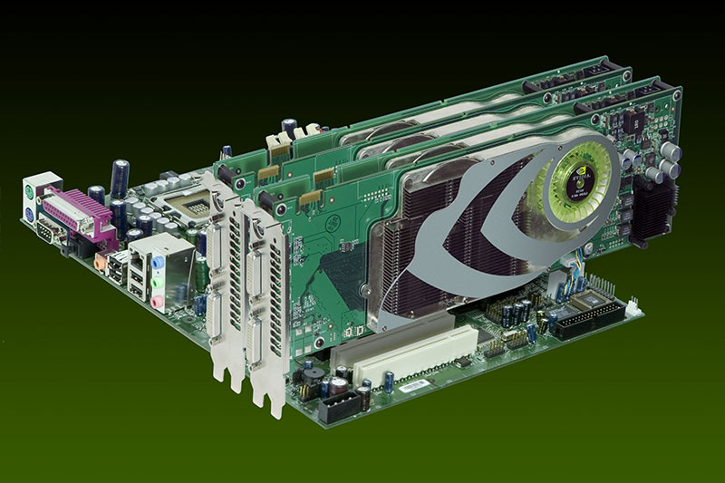
In the past we have seen dual GPU solutions on one PCB from manufacturers like Gigabyte or ASUS. But these were just GeForce 6600 designs which were not using such complex PCBs. The 7900 GTX is the biggest and baddest NVIDIA card around, of course it has a completely different range of requirements when it comes to power and signal stability.
So putting two GPUs on one PCB was out. The clever people at NVIDIA worked up a rather simple but ingenious solution - just stack two video cards, let them use only one slot connector and interconnect them with an own PCI-E bus. Each card has a little bridge device on it which connects the second card to the main PCI-E slot into which the card is plugged.

Add a second card, connect the two cards each with a SLI bridge and you have four interconnected GPUs which need only two slots.

However, since the power requirements of this little electrical heating are so immense, most Quad SLI systems are using 900W PSUs. At the NVIDIA press conference one NVIDIA spokesman was "actually pretty happy with the power consumption, we are only using 680W PSUs".
This brings us to another problem. Since the consumed power does not do any physical work, well except for the fans, it is dissipated as heat. And there's lots of it. NVIDIA uses a low-profile fan on each GPU. This means that each video card has its own fan, so the total number of coolers is four.
But to stay within their "thermal budget" NVIDIA had to reduce the clock rates of the 7900 GX2 down to 500 MHz Core and 605 MHz memory from the 7900 GTX's original 650 MHz / 800 MHz.
Each SLI card has 512 MB of video memory per GPU. Of course this means that one card consisting of two GPUs has 1 GB video memory onboard. But you can not just say "1 GB video card". The memories are completely separated. Each GPU has only access to its own 512 MB memory. There's no dynamic distribution based on need, like it is happening in your computer's main memory. This means that you can not use more than 512 MB video memory at one time in your application.

You really get something for your money. The PCB is the biggest consumer video card PCB I have seen in a long time. The small red card is a Sapphire X850 Pro.
The Cards
Let's take apart one of these GX2 cards.
Obviously one GX2 card is a double-height card. Because of its length it may be hard to install in some cases because there's very little space. In our Coolermaster case you had to insert the cards exactly straight into the case, otherwise they wouldn't plug into the PCI-Express connector.
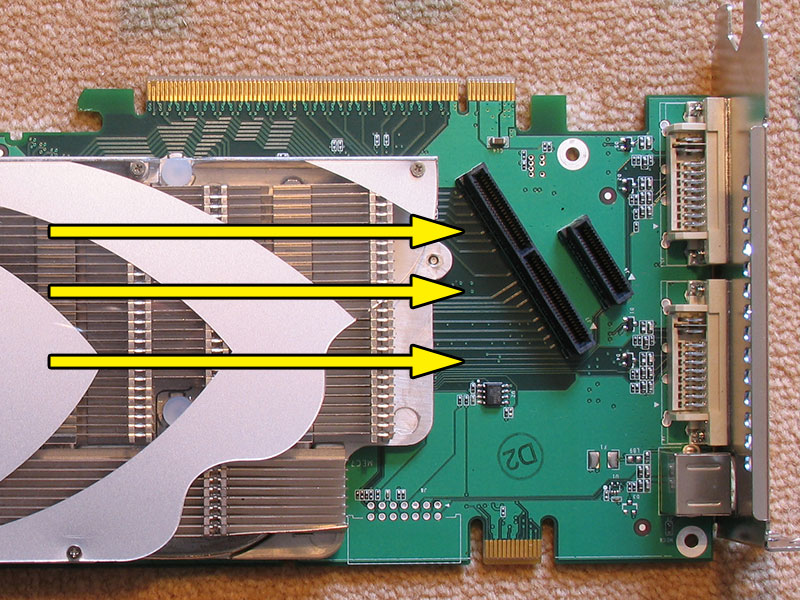
First we remove the "top" card which does not have its own PCI-Express connector.

This is the front of the card. A high-res version (around 2 MB) is here.

Here we see the back of the card. High-res.
With the top card gone we can now take a closer look at the second card which has the outputs and the slot connector.
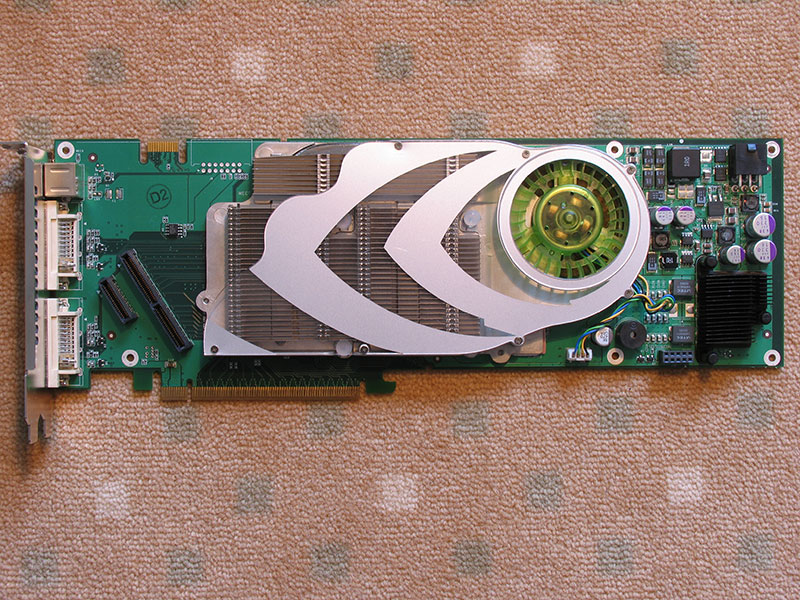
This is the front. High-res.
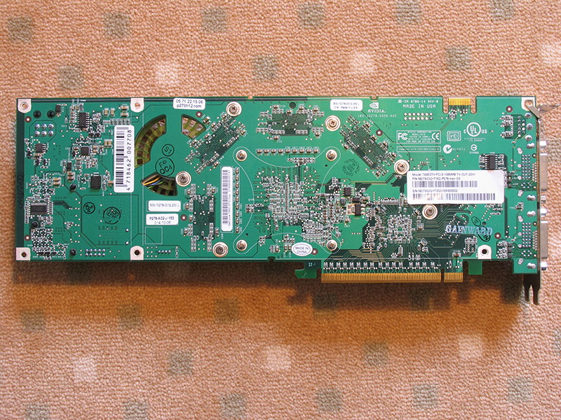
.. and the back. High-res.
A closer look
What is important with the PCB design is that the two card parts are interconnected by an own PCI-Express bus and an own SLI connector. Both are just sized down versions of the regular connectors.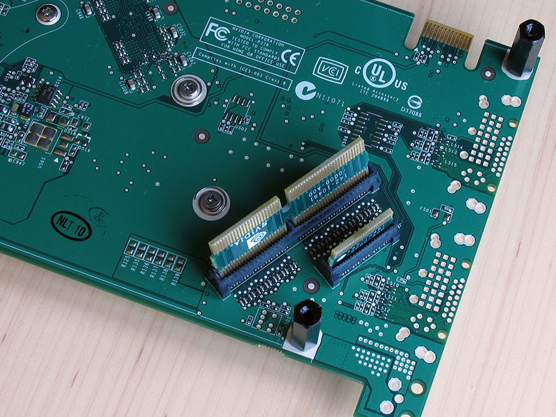
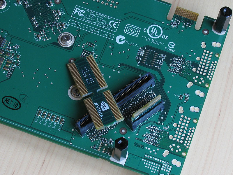
The little PCB on the left is a fully functional PCI-Express connector and to the right of it sits a PCB for the SLI bridge interface.
One little problem is that these two connectors block the outgoing airflow of one cooling fan. The reason why the connector is where it is now, is the PCB routing, all individual signals of the PCI-E bus have to have the same trace length, otherwise the bus becomes unstable.
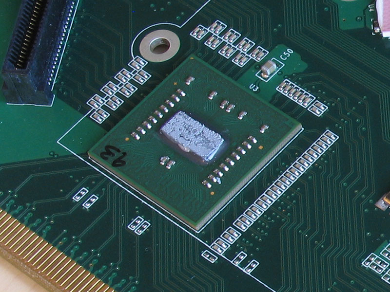
This PCI-E to PCI-E bridge chip is interfacing with the motherboard's PCI-Express bus on one side and on the other side it implements its own bus for the two cards (the two cards which are part of one GX2 card) to exchange data.
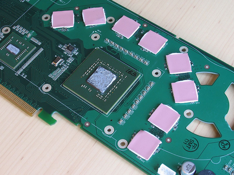
The memory is arranged on one side, closely around the GPU like we know it from all modern NVIDIA and ATI video cards.
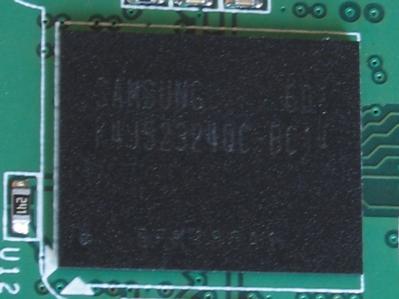
As memory chips Samsung K4J52324QC-BC14 is used. With a nominal speed of 1.4 ns it should run at least 700 MHz real clock.
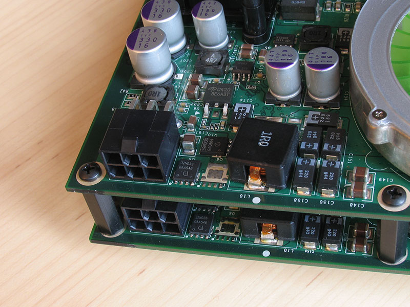
These are the power connectors. Each "card" needs its own supply of power which means you will need four power connectors for a Quad-SLI system. If your PSU doesn't have four connectors, which it most probably doesn't you can use a 5.25" to PCI-E power conversion cable.
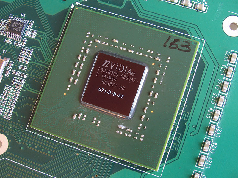
This is the heart of Quad-SLI, a G71-D-N GPU. The same as on the 7900 GT(X), the A2 stands for the revision.
As mentioned before, to make sure the cards don't overheat, NVIDIA chose to reduce the core clock by 150 MHz down to 500 MHz.
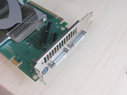
As output only DVI is available. If you spend so much money on video cards you better have a high-res LCD panel with DVI input. Of course wide-screen gaming is fully supported by the 7900 GX2 and after playing on the huge 30" Apple LCD I can only recommend it to everybody. Not only does it look great, it also gives you a bigger viewing angle, possibly showing an enemy which wouldn't have been visible on normal apect ratio - going wide-screen will give you more frags.
Our Patreon Silver Supporters can read articles in single-page format.
Apr 10th, 2025 22:40 EDT
change timezone
Latest GPU Drivers
New Forum Posts
- Lossless scaling (1)
- The TPU UK Clubhouse (26075)
- Post your cooling. (219)
- water chiller vs 480mm rad with water loop i9 13th gen cooling (6)
- Your PC ATM (35340)
- (Some of) What I'd like to See From a Final Fantasy IX Remake (12)
- Folding Pie and Milestones!! (9467)
- I need help finding the correct vBIOS for my Chinese graphics card. It's an RX 580 (0)
- 7800x3D randomly hits 90C, readings make no sense? (10)
- TPU's F@H Team (20423)
Popular Reviews
- The Last Of Us Part 2 Performance Benchmark Review - 30 GPUs Compared
- ASRock Z890 Taichi OCF Review
- Thermaltake TR100 Review
- Zotac GeForce RTX 5070 Ti Amp Extreme Review
- Sapphire Radeon RX 9070 XT Pulse Review
- Acer Predator GM9000 2 TB Review
- Sapphire Radeon RX 9070 XT Nitro+ Review - Beating NVIDIA
- Upcoming Hardware Launches 2025 (Updated Apr 2025)
- PowerColor Radeon RX 9070 Hellhound Review
- MCHOSE L7 Pro Review
Controversial News Posts
- NVIDIA GeForce RTX 5060 Ti 16 GB SKU Likely Launching at $499, According to Supply Chain Leak (175)
- MSI Doesn't Plan Radeon RX 9000 Series GPUs, Skips AMD RDNA 4 Generation Entirely (146)
- Microsoft Introduces Copilot for Gaming (124)
- AMD Radeon RX 9070 XT Reportedly Outperforms RTX 5080 Through Undervolting (119)
- NVIDIA Reportedly Prepares GeForce RTX 5060 and RTX 5060 Ti Unveil Tomorrow (115)
- NVIDIA Sends MSRP Numbers to Partners: GeForce RTX 5060 Ti 8 GB at $379, RTX 5060 Ti 16 GB at $429 (104)
- Nintendo Confirms That Switch 2 Joy-Cons Will Not Utilize Hall Effect Stick Technology (103)
- Over 200,000 Sold Radeon RX 9070 and RX 9070 XT GPUs? AMD Says No Number was Given (100)