 39
39
Phison E31 PCIe 5.0 SSD Engineering Sample Preview - Impressive Efficiency
Test Setup »The Drive
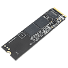
The drive is designed for the M.2 2280 form factor, which makes it 22 mm wide and 80 mm long.
PCI-Express 5.0 x4 is used as the host interface to the rest of the system, which doubles the theoretical bandwidth compared to PCIe 4.0 x4.
On the PCB you'll find the controller and two flash chips, a DRAM cache chip is not included.
Chip Component Analysis
The Phison E31 is the company's second PCI-Express 5.0 controller. It supports a four-lane configuration and four flash channels, it's a cost-optimized DRAM-less design. The controller is produced using a 7 nm process at TSMC Taiwan.
The two flash chips are Toshiba 218-layer 3D TLC NAND. Each chip has a capacity of 1 TB.
Mar 10th, 2025 07:13 EDT
change timezone
Latest GPU Drivers
New Forum Posts
- What are you playing? (23122)
- RX 9070 availability (124)
- Looking for Palit 5090 Gamerock OC BIOS (10)
- I'm looking for a good tool to make the 3D scanning of my mini-pc using the photogrammetry and my Kinect 2. (40)
- Do you use NVIDIA's Studio Drivers? (28)
- Nvidia's GPU market share hits 90% in Q4 2024 (gets closer to full monopoly) (764)
- It's happening again, melting 12v high pwr connectors (1016)
- RX 9000 series GPU Owners Club (35)
- What is a good real price for the RTX 5090? (18)
- RTX 5090 ridiculous price! (194)
Popular Reviews
- Sapphire Radeon RX 9070 XT Nitro+ Review - Beating NVIDIA
- XFX Radeon RX 9070 XT Mercury OC Magnetic Air Review
- ASUS Radeon RX 9070 TUF OC Review
- MSI MAG B850 Tomahawk Max Wi-Fi Review
- NVIDIA GeForce RTX 5080 Founders Edition Review
- NVIDIA GeForce RTX 5070 Founders Edition Review
- Corsair Vengeance RGB CUDIMM DDR5-8800 48 GB CL42 Review
- AMD Ryzen 7 9800X3D Review - The Best Gaming Processor
- ASUS GeForce RTX 5070 Ti TUF OC Review
- MSI GeForce RTX 5070 Ti Gaming Trio OC+ Review
Controversial News Posts
- NVIDIA GeForce RTX 50 Cards Spotted with Missing ROPs, NVIDIA Confirms the Issue, Multiple Vendors Affected (513)
- AMD Plans Aggressive Price Competition with Radeon RX 9000 Series (277)
- AMD Radeon RX 9070 and 9070 XT Listed On Amazon - One Buyer Snags a Unit (261)
- AMD RDNA 4 and Radeon RX 9070 Series Unveiled: $549 & $599 (260)
- AMD Mentions Sub-$700 Pricing for Radeon RX 9070 GPU Series, Looks Like NV Minus $50 Again (248)
- NVIDIA Investigates GeForce RTX 50 Series "Blackwell" Black Screen and BSOD Issues (244)
- AMD Radeon RX 9070 and 9070 XT Official Performance Metrics Leaked, +42% 4K Performance Over Radeon RX 7900 GRE (195)
- AMD Radeon RX 9070-series Pricing Leaks Courtesy of MicroCenter (158)


