 26
26
PNY GeForce RTX 4060 Ti Verto Review
(26 Comments) »Introduction
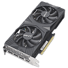
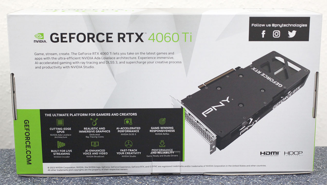
PNY GeForce RTX 4060 Ti 8 GB Verto Dual Fan is the company's most affordable custom-design graphics card based on NVIDIA's latest entry to the mainstream segment. It launches at exactly $399, or the MSRP for the RTX 4060 Ti, hence we are allowed to present our review a day before those of premium custom-design cards priced above the MSRP. The Verto Dual Fan by PNY covers all the basics of the graphics card, and is designed for those who just want an RTX 4060 Ti that they can install and get gaming. The card runs the GPU at reference speeds, and offers the added bonus of a legacy 8-pin PCIe power connector, so even those with entry-level legacy PSUs can get in on the action.

The GeForce RTX 4060 Ti is part of a three-model RTX 4060-series. This is the primary model with 8 GB memory, there is going to be a 16 GB model bound for July, alongside the more affordable RTX 4060 (non-Ti). The RTX 4060 Ti is based on the newer 5 nm AD106 silicon, which it nearly maxes out, enabling 34 out of 36 SM (streaming multiprocessors), which work out to 4,352 CUDA cores, 34 RT cores, 136 Tensor cores, those many TMUs, and 48 ROPs. While the card comes with the same 8 GB memory size as its predecessor, the RTX 3060 Ti, its memory bus width is generationally halved to 128-bit. NVIDIA introduced several architectural improvements that reduce the dependency on memory bandwidth by deploying large on-die caches, which we'll detail in the next page. Another area of cost-cutting is the PCIe interface, which now runs at Gen 4 x8.
The main play for the RTX 4060 Ti is that it still offers all of the good stuff NVIDIA introduced with the RTX 40-series Ada architecture, including the switch to the new 5 nm foundry process, which vastly reduces power draw; support for DLSS 3 Frame Generation technology, which conjures up entire alternative frames purely using AI, and without involving the graphics rendering machinery; and generational improvements to the ray tracing performance. Ada debuts the third generation of NVIDIA's path-breaking RTX real time ray tracing technology, and the fourth generation of NVIDIA's AI acceleration.
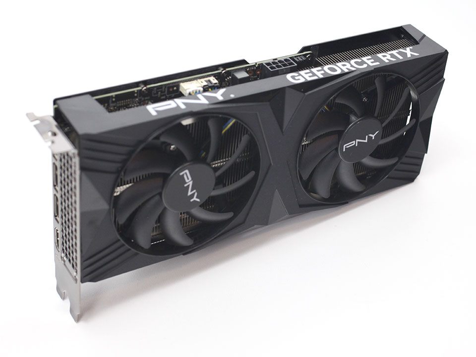
The PNY RTX 4060 Ti Verto Dual Fan comes with a basic board design, and uses a compact, dual-slot cooling solution. An aluminium fin-stack heatsink cools the GPU and other hot components, which is ventilated by a pair of fans. A basic plastic cooler shroud and metal backplate are used to complete the look. What you get at its $399 MSRP is everything the RTX 4060 Ti has to offer on its own.
| Price | Cores | ROPs | Core Clock | Boost Clock | Memory Clock | GPU | Transistors | Memory | |
|---|---|---|---|---|---|---|---|---|---|
| RTX 2060 | $180 | 1920 | 48 | 1365 MHz | 1680 MHz | 1750 MHz | TU106 | 10800M | 6 GB, GDDR6, 192-bit |
| RX Vega 64 | $320 | 4096 | 64 | 1247 MHz | 1546 MHz | 953 MHz | Vega 10 | 12500M | 8 GB, HBM2, 2048-bit |
| RX 5700 XT | $180 | 2560 | 64 | 1605 MHz | 1755 MHz | 1750 MHz | Navi 10 | 10300M | 8 GB, GDDR6, 256-bit |
| RTX 3050 | $260 | 2560 | 32 | 1552 MHz | 1777 MHz | 1750 MHz | GA106 | 12000M | 8 GB, GDDR6, 128-bit |
| RTX 2070 | $230 | 2304 | 64 | 1410 MHz | 1620 MHz | 1750 MHz | TU106 | 10800M | 8 GB, GDDR6, 256-bit |
| RX 6600 | $210 | 1792 | 64 | 2044 MHz | 2491 MHz | 1750 MHz | Navi 23 | 11060M | 8 GB, GDDR6, 128-bit |
| RTX 3060 | $300 | 3584 | 48 | 1320 MHz | 1777 MHz | 1875 MHz | GA106 | 12000M | 12 GB, GDDR6, 192-bit |
| RTX 4060 | $300 | 3072 | 32 | 1830 MHz | 2460 MHz | 2125 MHz | AD107 | unknown | 8 GB, GDDR6, 128-bit |
| RX 6600 XT | $250 | 2048 | 64 | 2359 MHz | 2589 MHz | 2000 MHz | Navi 23 | 11060M | 8 GB, GDDR6, 128-bit |
| Arc A750 | $250 | 3584 | 112 | 2050 MHz | N/A | 2000 MHz | ACM-G10 | 21700M | 8 GB, GDDR6, 256-bit |
| Arc A770 | $290 | 4096 | 128 | 2100 MHz | N/A | 2187 MHz | ACM-G10 | 21700M | 16 GB, GDDR6, 256-bit |
| RTX 2080 | $260 | 2944 | 64 | 1515 MHz | 1710 MHz | 1750 MHz | TU104 | 13600M | 8 GB, GDDR6, 256-bit |
| RTX 3060 Ti | $320 | 4864 | 80 | 1410 MHz | 1665 MHz | 1750 MHz | GA104 | 17400M | 8 GB, GDDR6, 256-bit |
| RTX 4060 Ti | $400 | 4352 | 48 | 2310 MHz | 2535 MHz | 2250 MHz | AD106 | 22900M | 8 GB, GDDR6, 128-bit |
| PNY RTX 4060 Ti Verto | $400 | 4352 | 48 | 2310 MHz | 2535 MHz | 2250 MHz | AD106 | 22900M | 8 GB, GDDR6, 128-bit |
| RX 6700 XT | $320 | 2560 | 64 | 2424 MHz | 2581 MHz | 2000 MHz | Navi 22 | 17200M | 12 GB, GDDR6, 192-bit |
| RTX 2080 Ti | $400 | 4352 | 88 | 1350 MHz | 1545 MHz | 1750 MHz | TU102 | 18600M | 11 GB, GDDR6, 352-bit |
| RTX 3070 | $350 | 5888 | 96 | 1500 MHz | 1725 MHz | 1750 MHz | GA104 | 17400M | 8 GB, GDDR6, 256-bit |
| RTX 3070 Ti | $420 | 6144 | 96 | 1575 MHz | 1770 MHz | 1188 MHz | GA104 | 17400M | 8 GB, GDDR6X, 256-bit |
Architecture
The Ada graphics architecture heralds the third generation of the NVIDIA RTX technology, an effort toward increasing the realism of game visuals by leveraging real-time ray tracing, without the enormous amount of compute power required to draw purely ray-traced 3D graphics. This is done by blending conventional raster graphics with ray traced elements such as reflections, lighting, and global illumination, to name a few. The 3rd generation of RTX introduces the new higher IPC "Ada" CUDA core, 3rd generation RT core, 4th generation Tensor core, and the new Optical Flow Processor, a component that plays a key role in generating new frames without involving the GPU's main graphics rendering pipeline.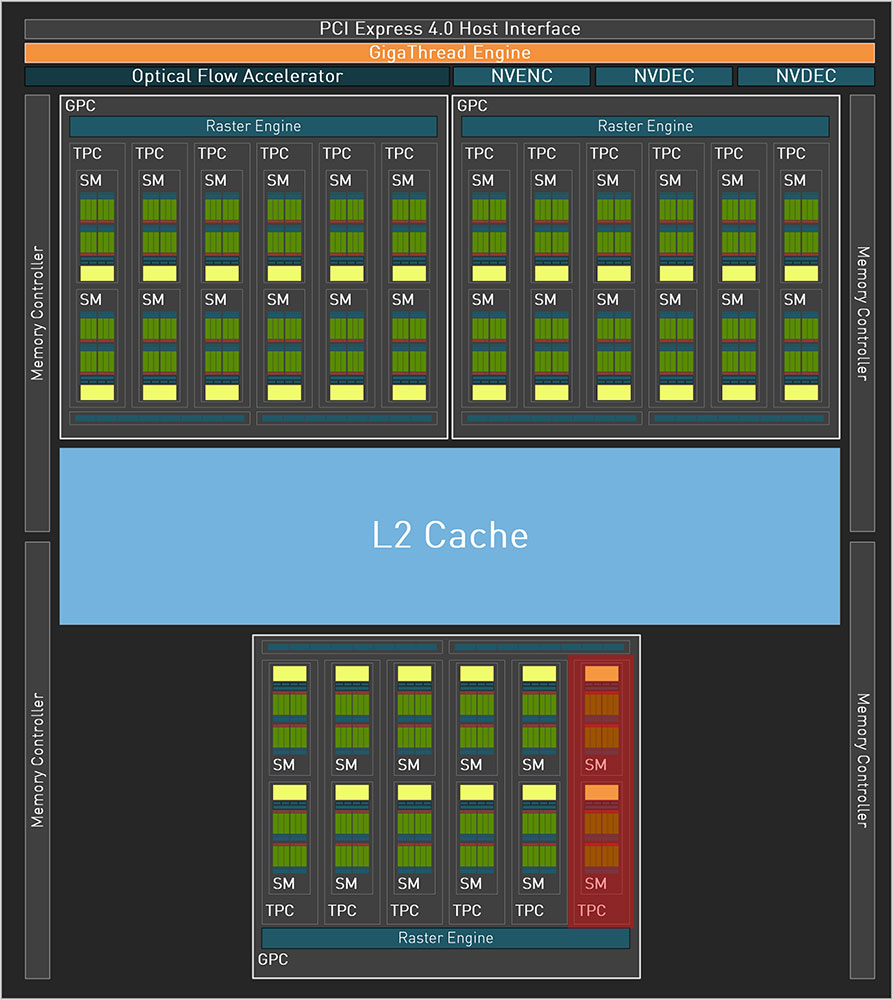
The GeForce Ada graphics architecture driving the RTX 4060 Ti leverages the TSMC 5 nm EUV foundry process to increase transistor counts. At the heart of this GPU is the new AD106 silicon, with a fairly high transistor count of 22.9 billion, which is almost double that of the previous-generation GA106, and still about 30% more than the GA104. The GPU features a generationally narrower PCI-Express 4.0 x8 host interface, and a 128-bit wide GDDR6 memory interface. This is causing some controversy, and we'll present NVIDIA's explanation below. The Optical Flow Accelerator (OFA) is an independent top-level component. The chip features one NVENC and one NVDEC unit.
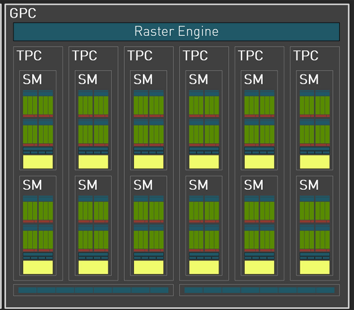
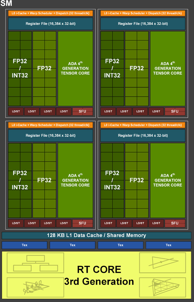
The essential component hierarchy is similar to past generations of NVIDIA GPUs. The AD106 silicon features 3 Graphics Processing Clusters (GPCs), each of these has all the SIMD and graphics rendering machinery, and is a small GPU in its own right. Each GPC shares a raster engine (geometry processing components) and two ROP partitions (each with eight ROP units). The GPC of the AD106 contains five Texture Processing Clusters (TPCs), the main number-crunching machinery. Each of these has two Streaming Multiprocessors (SM), and a Polymorph unit. Each SM contains 128 CUDA cores across four partitions. Half of these CUDA cores are pure-FP32; while the other half is capable of FP32 or INT32. The SM retains concurrent FP32+INT32 math processing capability. The SM also contains a 3rd generation RT core, four 4th generation Tensor cores, some cache memory, and four TMUs. There are 12 SM per GPC, so 1,536 CUDA cores, 48 Tensor cores, and 12 RT cores; per GPC. There are three such GPCs, which add up to 4,608 CUDA cores, 144 TMUs, 144 Tensor Cores, and 36 RT cores. Each GPC contributes 16 ROPs, so there are 48 ROPs on the silicon. The RTX 4060 Ti is carved out of the AD106 by disabling one TPC worth 256 CUDA cores. This yields 4,352 CUDA cores, 136 Tensor cores, 34 RT cores, and 136 TMUs. The ROP count is untouched at 48, as is the on-die L2 cache sees a slight reduction, which is 32 MB in size.
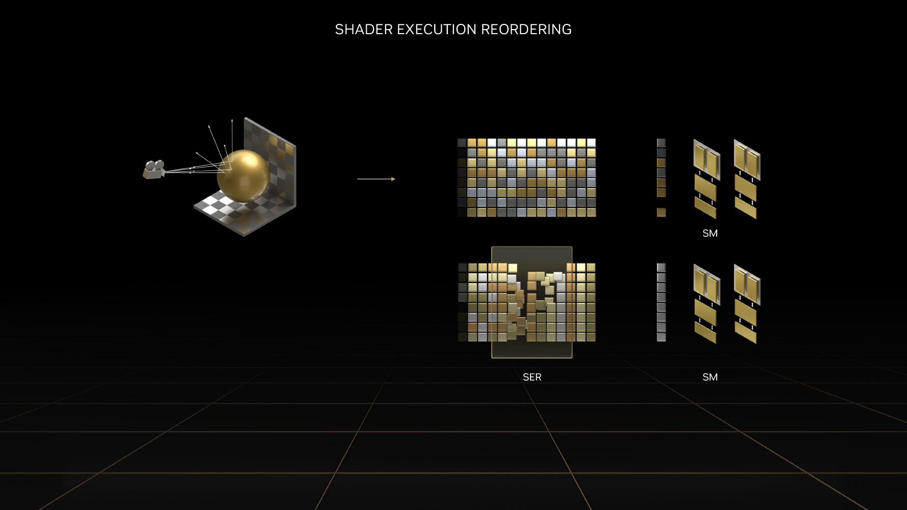
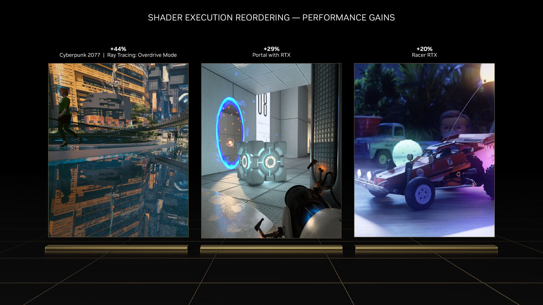
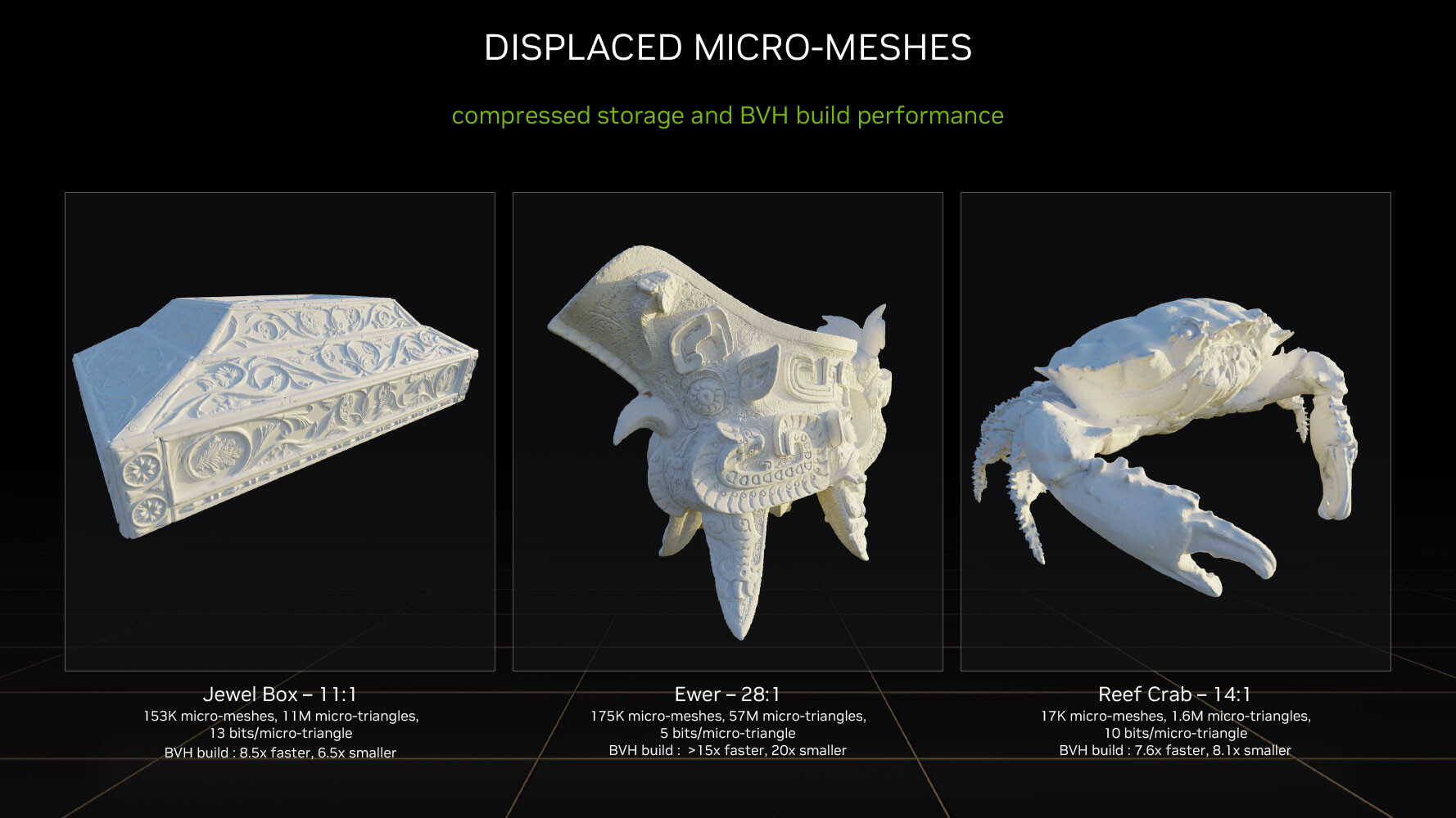
The 3rd generation RT core accelerates the most math-intensive aspects of real-time ray tracing, including BVH traversal. Displaced micro-mesh engine is a revolutionary feature introduced with the new 3rd generation RT core. Just as mesh shaders and tessellation have had a profound impact on improving performance with complex raster geometry, allowing game developers to significantly increase geometric complexity; DMMs is a method to reduce the complexity of the bounding-volume hierarchy (BVH) data-structure, which is used to determine where a ray hits geometry. Previously, the BVH had to capture even the smallest details to properly determine the intersection point. Ada's ray tracing architecture also receives a major performance uplift from Shader Execution Reordering (SER), a software-defined feature that requires awareness from game-engines, to help the GPU reorganize and optimize worker threads associated with ray tracing.
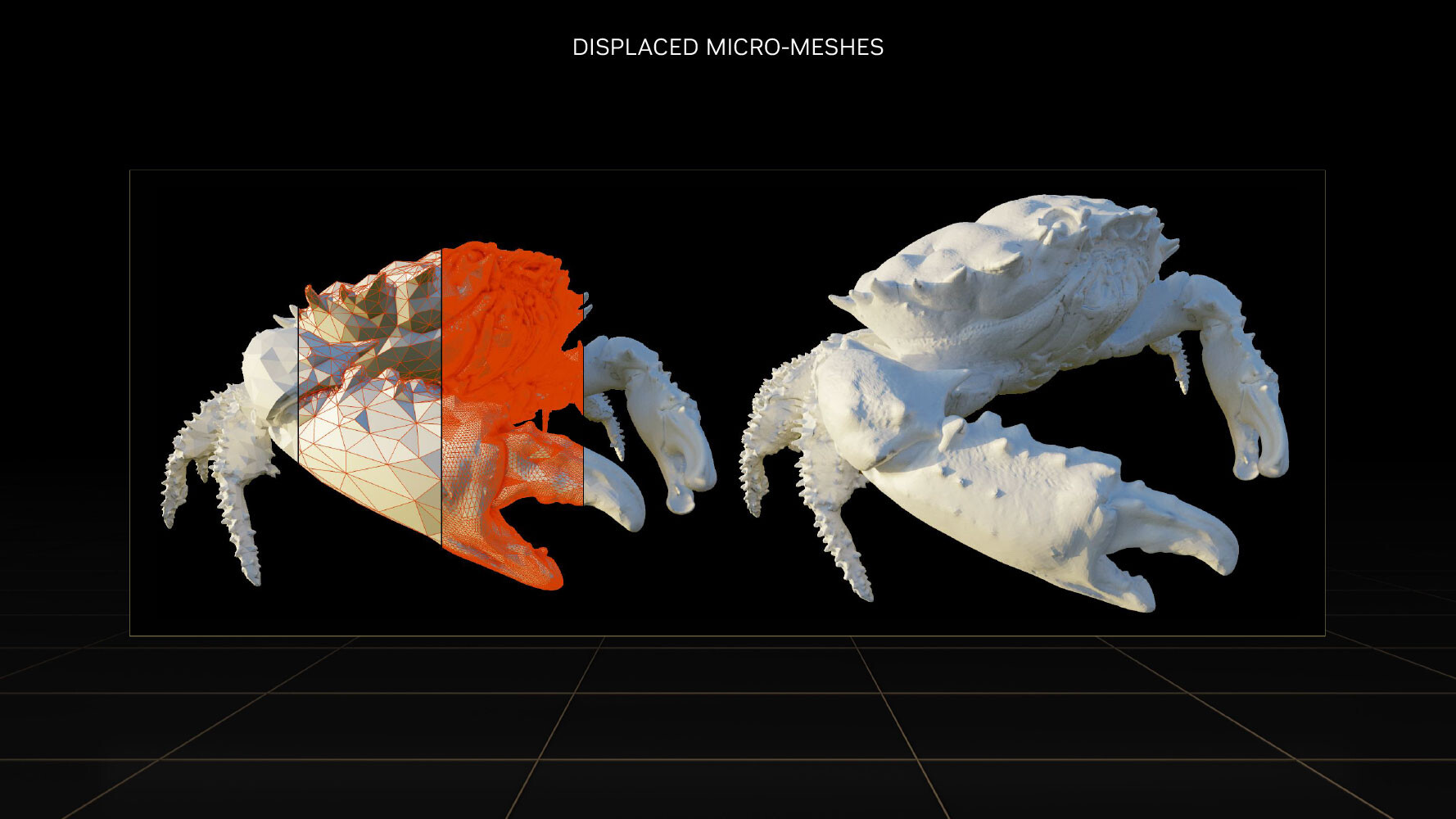
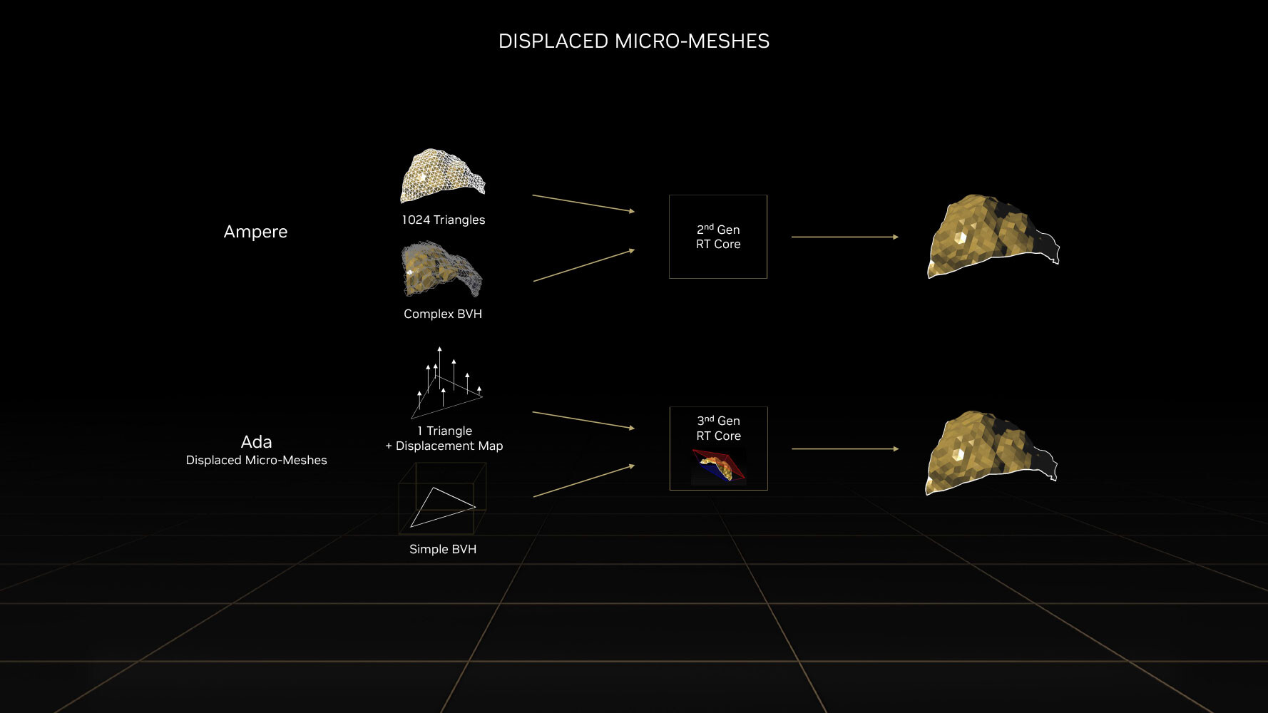
The BVH now needn't have data for every single triangle on an object, but can represent objects with complex geometry as a coarse mesh of base triangles, which greatly simplifies the BVH data structure. A simpler BVH means less memory consumed and helps to greatly reduce ray tracing CPU load, because the CPU only has to generate a smaller structure. With older "Ampere" and "Turing" RT cores, each triangle on an object had to be sampled at high overhead, so the RT core could precisely calculate ray intersection for each triangle. With Ada, the simpler BVH, plus the displacement maps can be sent to the RT core, which is now able to figure out the exact hit point on its own. NVIDIA has seen 11:1 to 28:1 compression in total triangle counts. This reduces BVH compile times by 7.6x to over 15x, in comparison to the older RT core; and reducing its storage footprint by anywhere between 6.5 to 20 times. DMMs could reduce disk- and memory bandwidth utilization, utilization of the PCIe bus, as well as reduce CPU utilization. NVIDIA worked with Simplygon and Adobe to add DMM support for their tool chains.
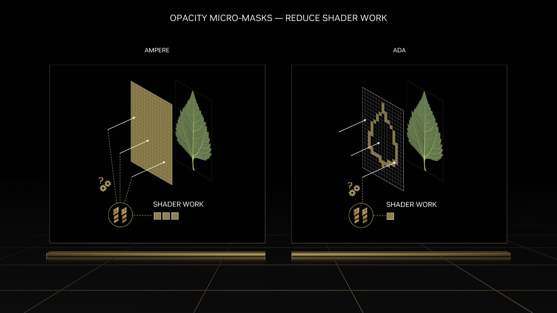
Opacity Micro Meshes (OMM) is a new feature introduced with Ada to improve rasterization performance, particularly with objects that have alpha (transparency data). Most low-priority objects in a 3D scene, such as leaves on a tree, are essentially rectangles with textures on the leaves where the transparency (alpha) creates the shape of the leaf. RT cores have a hard time intersecting rays with such objects, because they're not really in the shape that they appear (they're really just rectangles with textures that give you the illusion of shape). Previous-generation RT cores had to have multiple interactions with the rendering stage to figure out the shape of a transparent object, because they couldn't test for alpha by themselves.
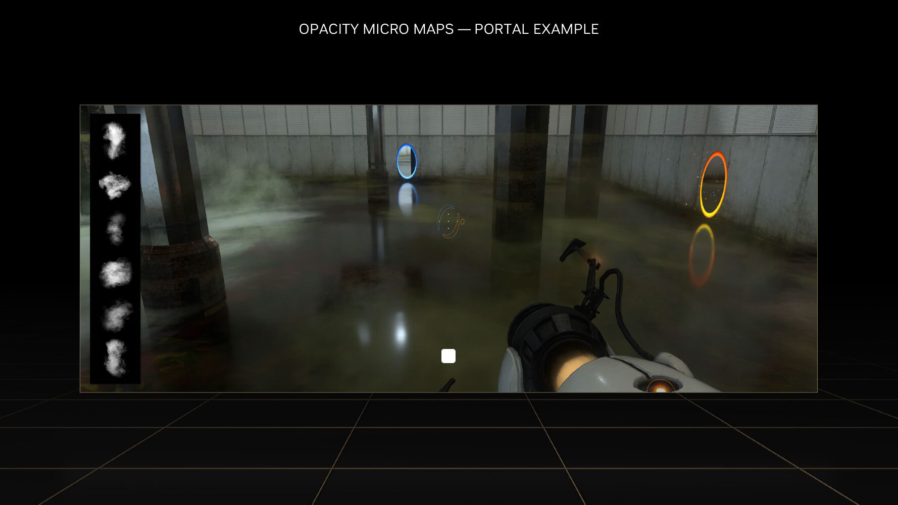
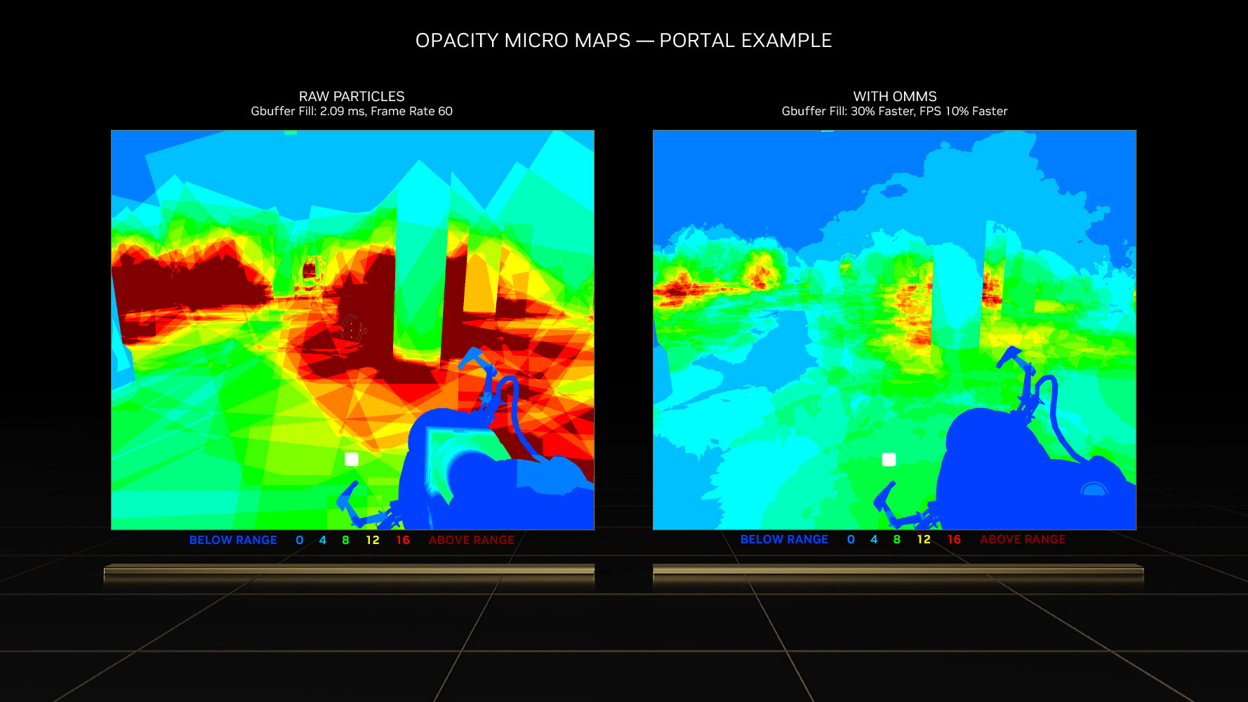
This has been solved by using OMMs. Just as DMMs simplify geometry by creating meshes of micro-triangles; OMMs create meshes of rectangular textures that align with parts of the texture that aren't alpha, so the RT core has a better understanding of the geometry of the object, and can correctly calculate ray intersections. This has a significant performance impact on shading performance in non-RT applications, too. Practical applications of OMMs aren't just low-priority objects such as vegetation, but also smoke-sprites and localized fog. Traditionally there was a lot of overdraw for such effects, because they layered multiple textures on top of each other, that all had to be fully processed by the shaders. Now only the non-opaque pixels get executed—OMMs provide a 30 percent speedup with graphics buffer fill-rates, and a 10 percent impact on frame-rates.
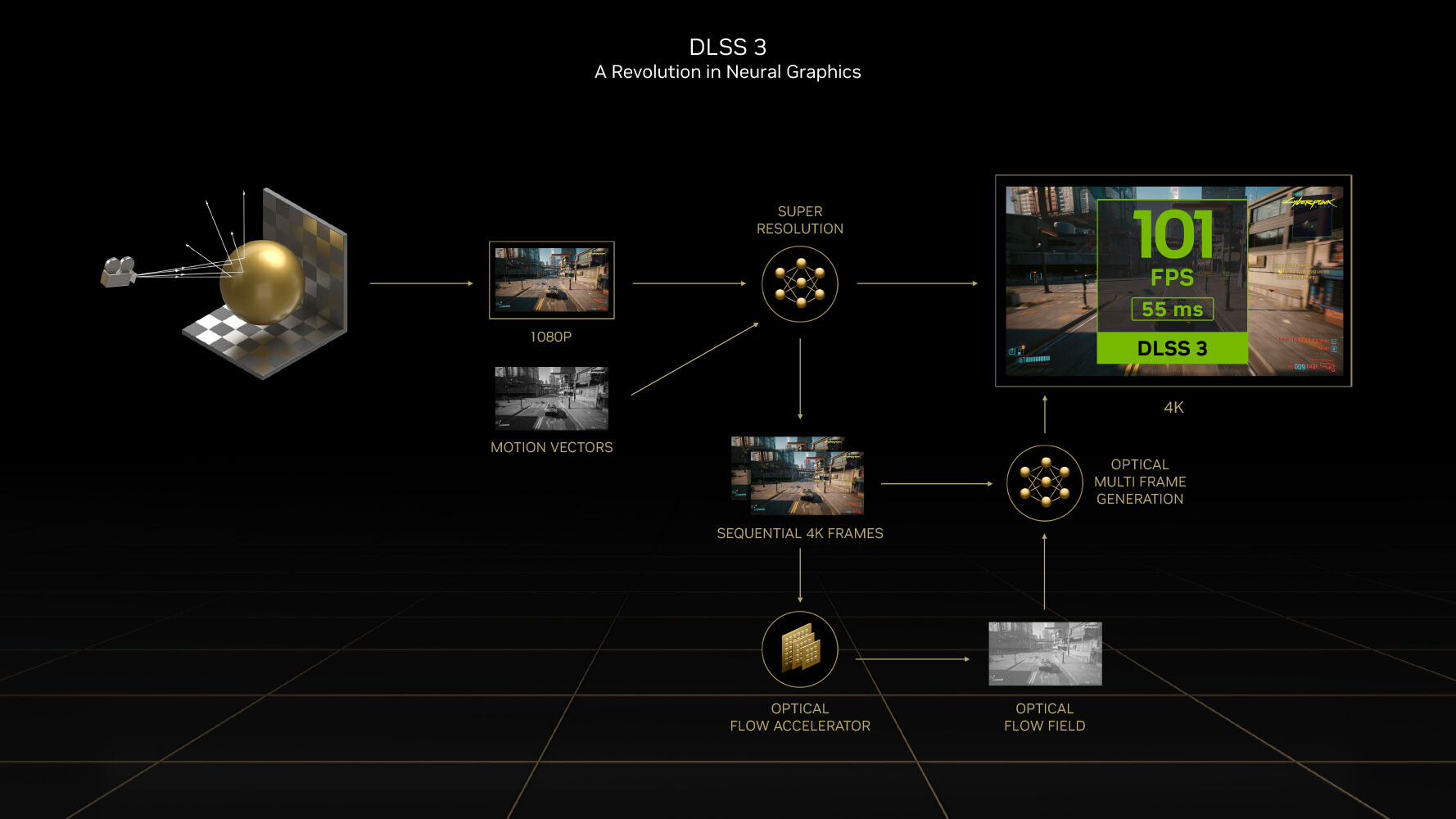
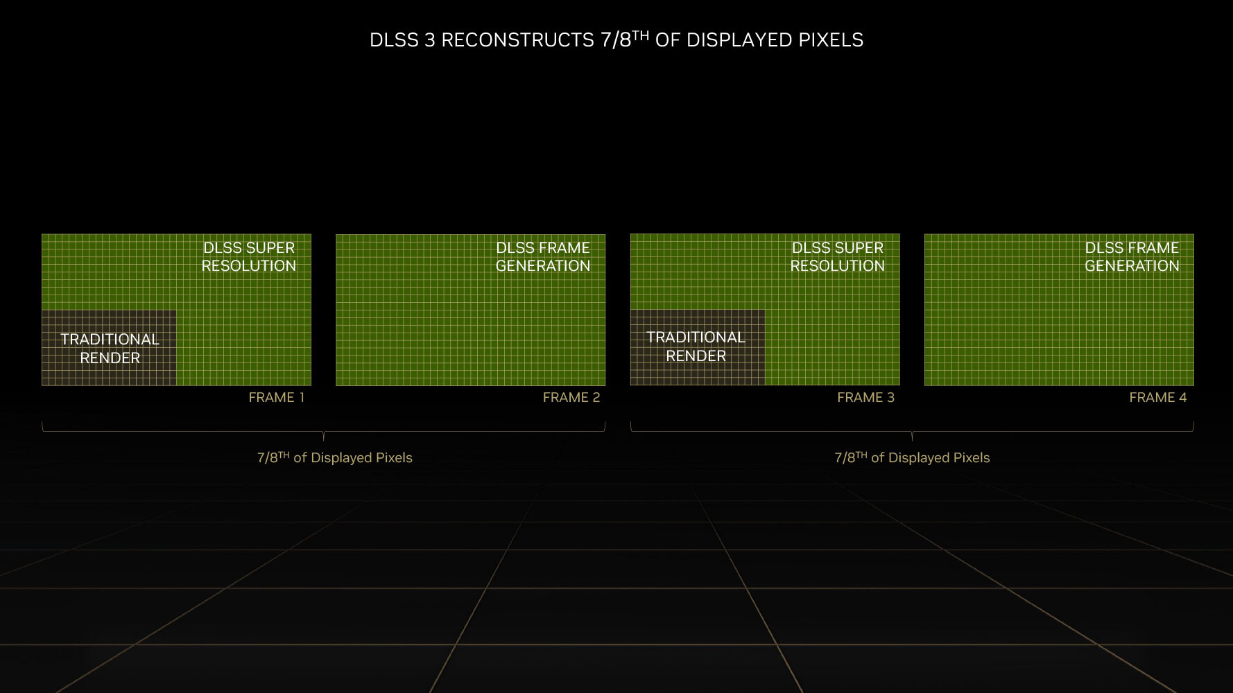
DLSS 3 introduces a revolutionary new feature that promises a doubling in frame-rate at comparable quality, it's called AI frame-generation. While it has all the features of DLSS 2 and its AI super-resolution (scaling up a lower-resolution frame to native resolution with minimal quality loss); DLSS 3 can generate entire frames simply using AI, without involving the graphics rendering pipeline. Later in the article, we will show you DLSS 3 in action.
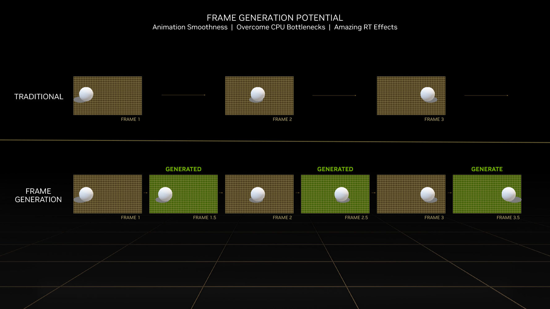
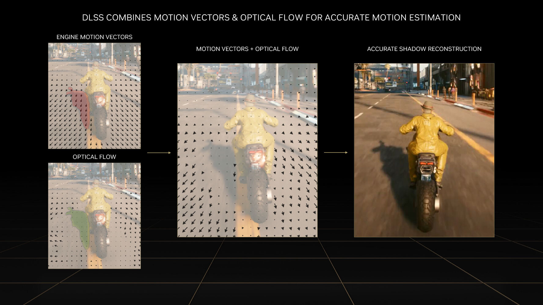
Every alternating frame with DLSS 3 is hence AI-generated, without being a replica of the previous rendered frame. This is possible only on the Ada graphics architecture, because of a hardware component called the optical flow accelerator (OFA), which assists in predicting what the next frame could look like, by creating what NVIDIA calls an optical flow-field. OFA ensures that the DLSS 3 algorithm isn't confused by static objects in a rapidly-changing 3D scene (such as a race sim). The process heavily relies on the performance uplift introduced by the FP8 math format of the 4th generation Tensor core. A third key ingredient of DLSS 3 is Reflex. By reducing the rendering queue to zero, Reflex plays a vital role in ensuring that frame-times with DLSS 3 are at an acceptable level, and a render-queue doesn't confuse the upscaler. A combination of OFA and the 4th Gen Tensor core is why the Ada architecture is required to use DLSS 3, and why it won't work on older architectures.
Ada Rebalanced Memory Subsystem
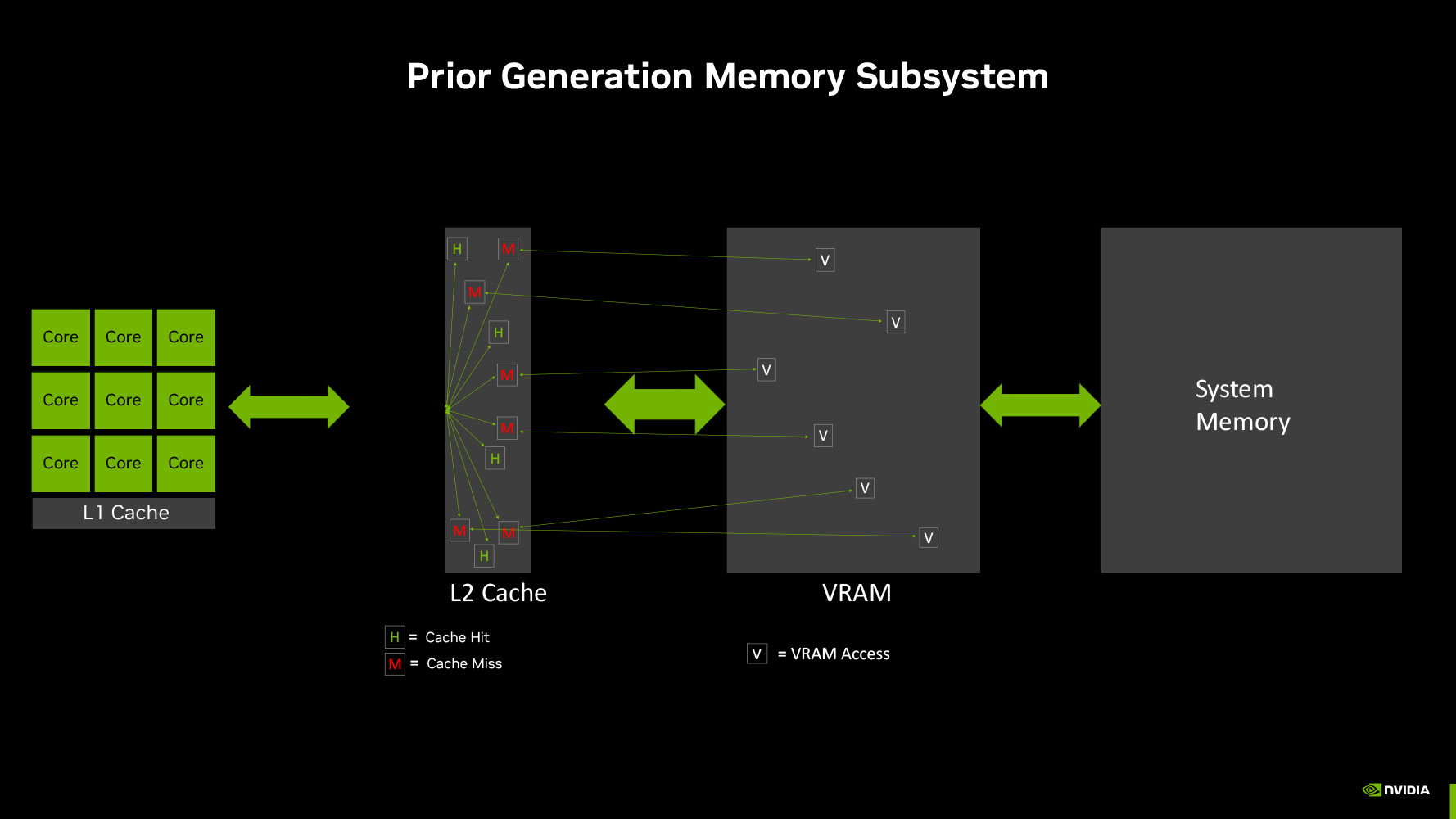
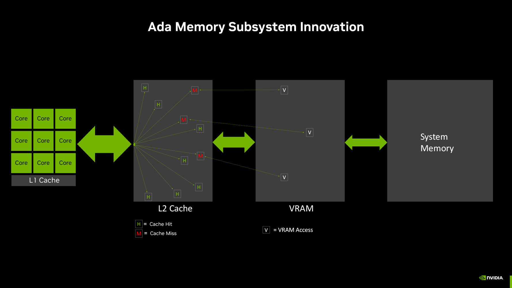
The previous-generation GeForce RTX 3060 Ti featured a 256-bit wide GDDR6 memory interface driving its 8 GB of 14 Gbps-rated GDDR6 memory (448 GB/s memory bandwidth), which has caused some controversy with the new RTX 4060 Ti using a narrower 128-bit wide memory interface to drive 8 GB of 18 Gbps memory (288 GB/s bandwidth). With the new Ada Lovelace graphics architecture, NVIDIA has tried to re-balance the memory sub-system such that there's dependence on larger on-die caches, allowing NVIDIA to narrow down the GPU's GDDR6 memory interface. The obvious benefit of this to NVIDIA is reduced costs, let's make no mistake about it, but NVIDIA maintains that this isn't a big problem for the GPU.
The last-level cache, or L2 cache, of NVIDIA Ada GPUs is anywhere between 8-10 times larger than the ones on the previous-generation Ampere GPUs. The AD106 silicon powering the RTX 4060 Ti has a 32 MB L2 cache, compared to the 4 MB of the GA104 silicon powering the RTX 3060 Ti. NVIDIA illustrated an example of how a the larger on-die LLC reduces video memory pressure (trips to GDDR6) by anywhere between 40% to 60% on the same GPU, by soaking up a larger number of memory access requests by the shaders.
The L2 cache is unified victim cache to the GPU's various GPCs and their local TPCs. Data that isn't hot enough (frequently accessed enough) to be resident on the small L1 caches of the SM, is ejected to the L2 cache, and depending on its heat, pushed to the GDDR6 video memory. The L2 cache is an order of magnitude faster than than video memory in terms of latency, and so having frequently-accessed data reside there offers a considerable benefit.
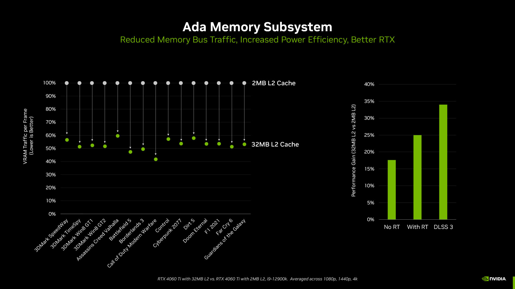
As we mentioned earlier from NVIDIA's claims, this re-balancing of the memory sub-system between the on-die LLC and video memory lowers the GPU's access to the latter by as much as 60%, which means the GPU can make do with a narrower 128-bit wide GDDR6 memory bus. With the 4060 Ti, NVIDIA has used generationally faster 18 Gbps memory chips. NVIDIA developed a new means of presenting the memory bandwidth that takes into account the contribution of the L2 cache, its hit-rate, and the consequent reduction in video memory traffic. While the memory bandwidth of the RTX 4060 Ti is 288 GB/s, NVIDIA claims that its "effective bandwidth" is 554 GB/s (23% higher than the 448 GB/s memory bandwidth of the RTX 3060 Ti). It's interesting to point out that NVIDIA has used "effective bandwidth" figures in the past to highlight its lossless memory compression technologies, but has never been this vocal about it.
Packaging
The Card
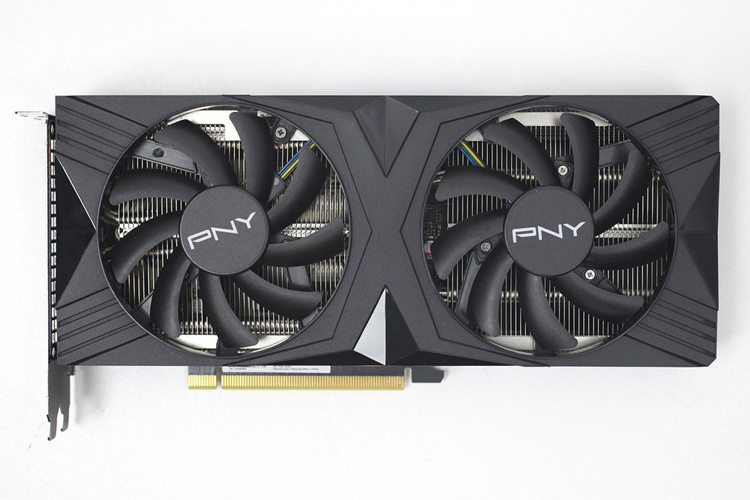
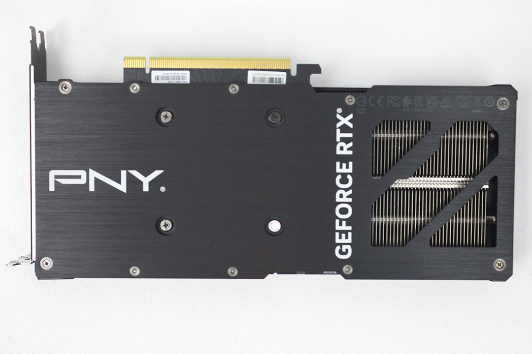
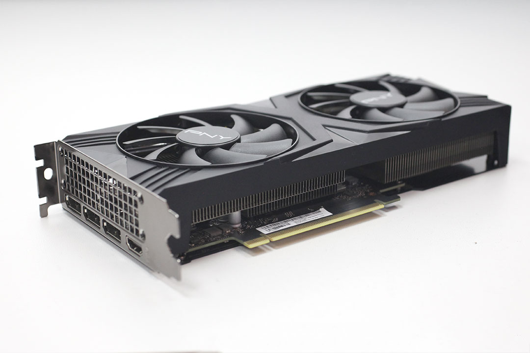
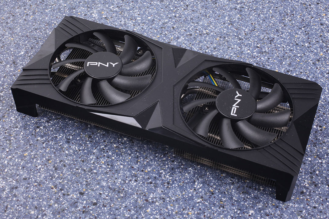
The PNY RTX 4060 Ti Verto comes with a mostly-black color theme that has some white highlights on it from the PNY and GeForce logos. There's a cutout for air to flow through, the main cooler shroud is made from plastic while the backplate is made of metal.
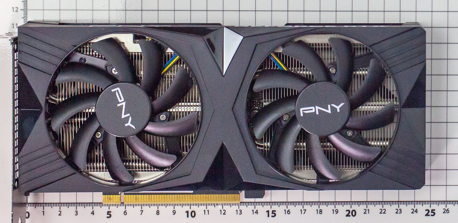
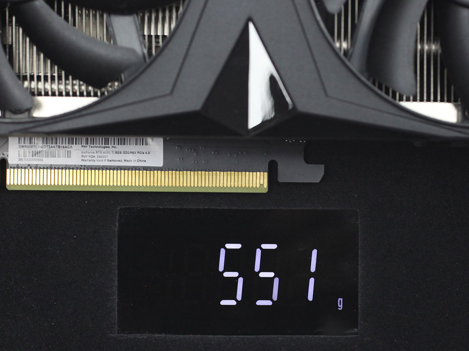
Dimensions of the card are 24.5 x 11.5 cm, and it weighs 551 g.
Installation requires two slots in your system.
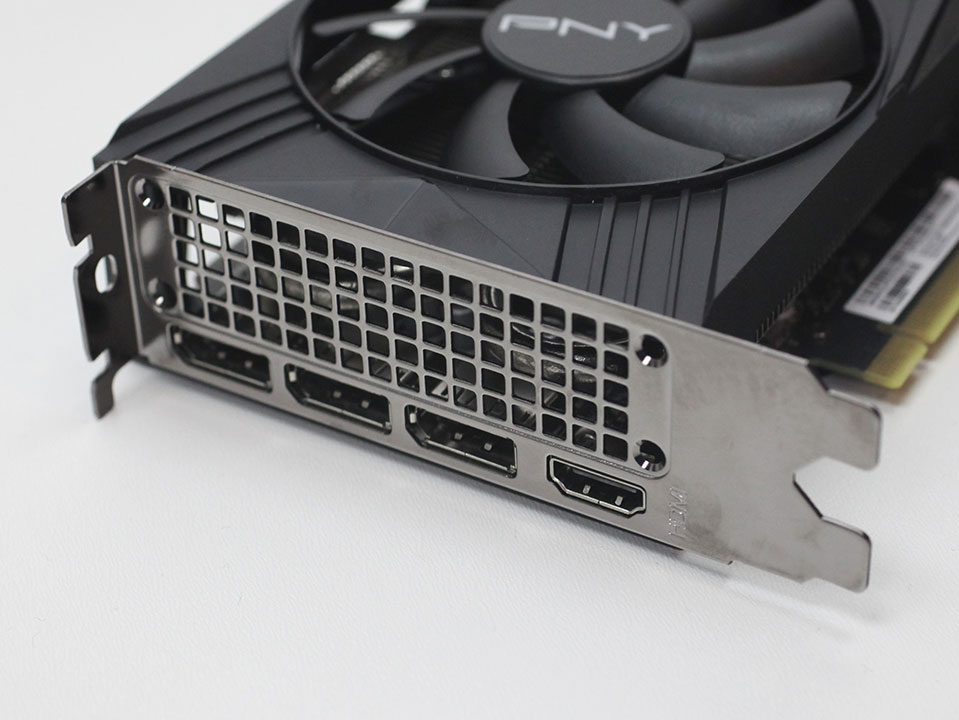
Display connectivity includes three standard DisplayPort 1.4a ports and one HDMI 2.1a (same as Ampere).
The new 8th Gen NVENC now accelerates AV1 encoding, besides HEVC. You also get an "optical flow accelerator" unit that is able to calculate intermediate frames for videos, to smooth playback. The same hardware unit is used for frame generation in DLSS 3.
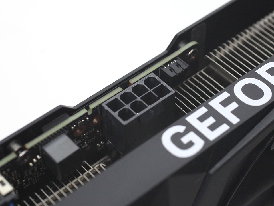
The card uses a single 8-pin power connector, which, together with the PCIe slot, is specified for up to 225 W power draw. Some other RTX 4070 cards like the NVIDIA Founders Edition come with the new 16-pin connector, but they are limited to the same power draw levels. NVIDIA has given their partners free choice on what connector they use, and I suspect the classic 8-pin is a little bit cheaper to implement.
Teardown
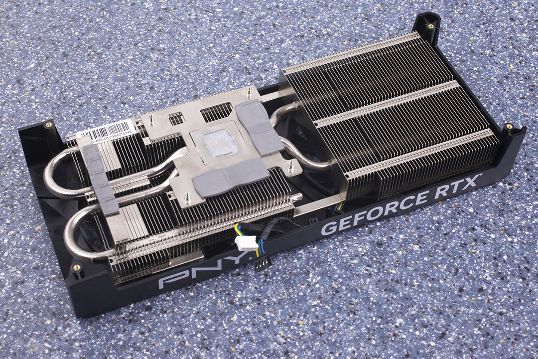
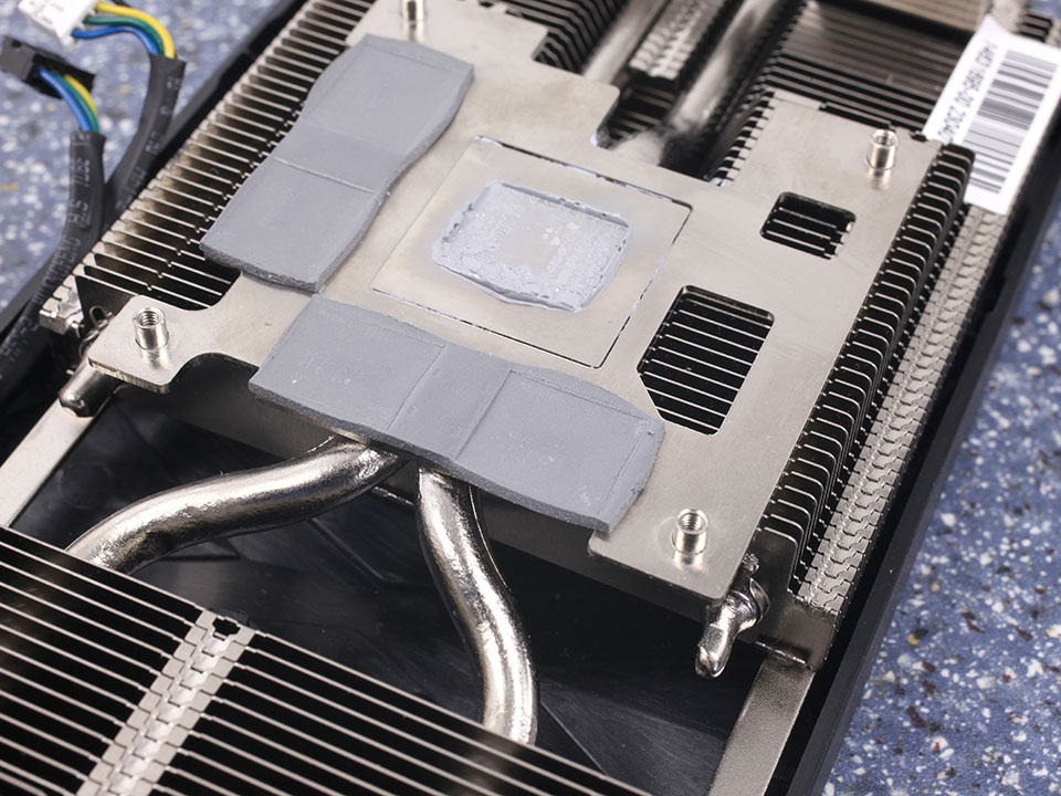
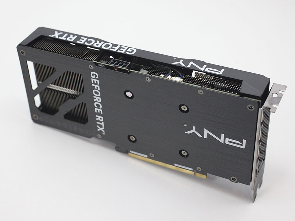
PNY's heatsink uses two heatpipes to keep the card cool. The main cooler also provides cooling for the memory chips and VRM circuitry.
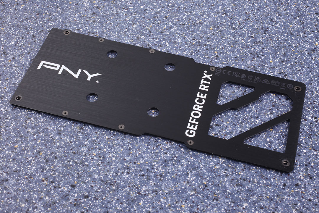
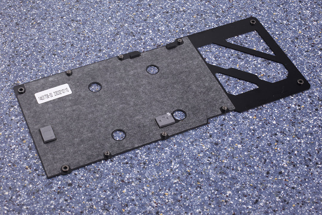
The metal backplate protects the card against damage during installation and handling.
High-resolution PCB Pictures
These pictures are for the convenience of volt modders and people who would like to see all the finer details on the PCB. Feel free to link back to us and use these in your articles, videos or forum posts.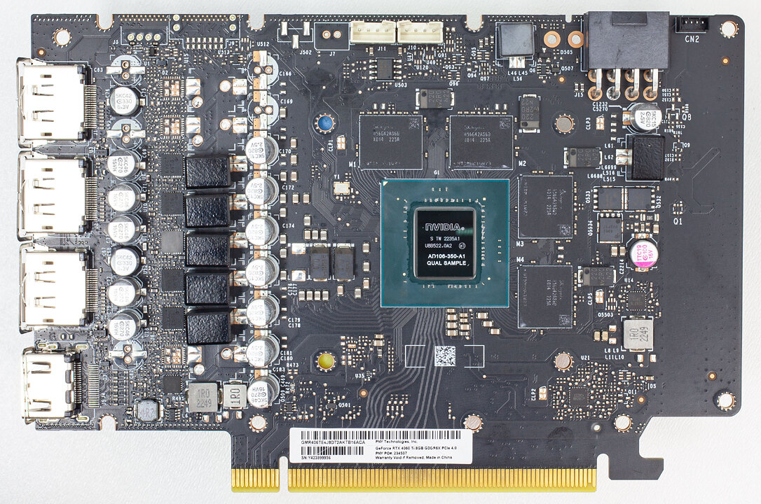
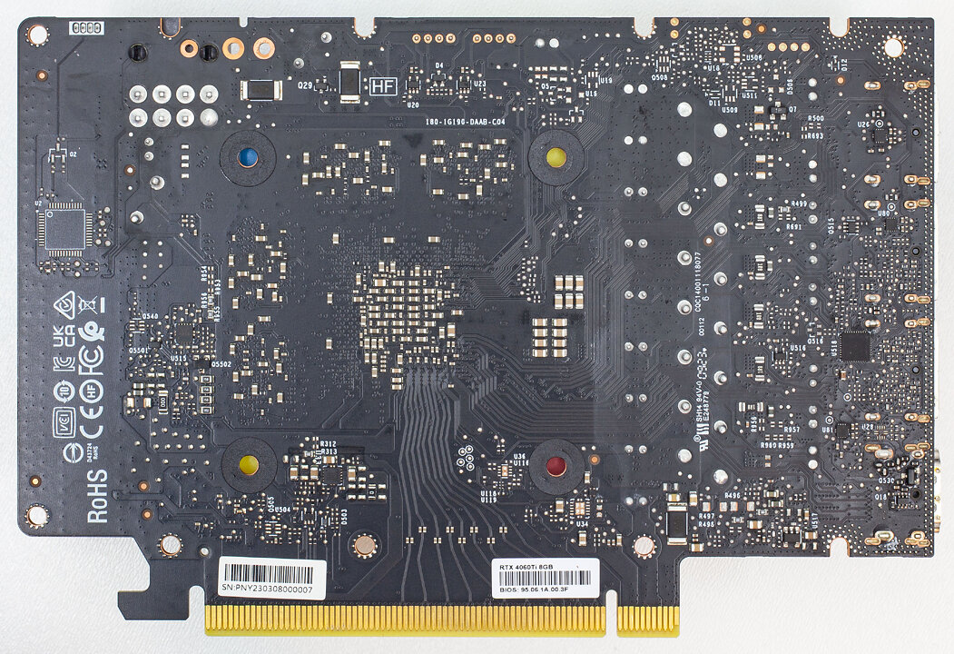
High-resolution versions are also available (front, back).
Our Patreon Silver Supporters can read articles in single-page format.
May 5th, 2025 05:16 EDT
change timezone
Latest GPU Drivers
New Forum Posts
- Low budget psu for medium high loads (under 400 watt usage) (23)
- Windows 12 (161)
- [AV1, AV2, AV3 codecs...] Have they given up on the AOMedia project? (18)
- RX 9000 series GPU Owners Club (641)
- Can't find BIOS for RX580 2048SP (5)
- Are the 8 GB cards worth it? (861)
- Best USB 3 hub chipsets (22)
- HP laptop upgrade ZBook G2 k4100 to Nvidia GTX 1070m and EliteBook 8770 (a few laptops) (33)
- (Mis)adventures in Storage Benchmarking (NVMe, Optane, Thunderbolt) (4)
- Choosing an Internal HDD (61)
Popular Reviews
- ASUS ROG Maximus Z890 Hero Review
- ASUS Radeon RX 9070 XT TUF OC Review
- Clair Obscur: Expedition 33 Performance Benchmark Review - 33 GPUs Tested
- Montech HS02 PRO Review
- NVIDIA GeForce RTX 5060 Ti 8 GB Review - So Many Compromises
- Seasonic Vertex GX 850 W Review
- Upcoming Hardware Launches 2025 (Updated Apr 2025)
- ASUS GeForce RTX 5090 Astral Liquid OC Review - The Most Expensive GPU I've Ever Tested
- Sapphire Radeon RX 9070 XT Nitro+ Review - Beating NVIDIA
- AMD Ryzen 7 9800X3D Review - The Best Gaming Processor
Controversial News Posts
- AMD Radeon RX 9060 XT to Roll Out 8 GB GDDR6 Edition, Despite Rumors (129)
- NVIDIA Sends MSRP Numbers to Partners: GeForce RTX 5060 Ti 8 GB at $379, RTX 5060 Ti 16 GB at $429 (128)
- NVIDIA Launches GeForce RTX 5060 Series, Beginning with RTX 5060 Ti This Week (115)
- Nintendo Confirms That Switch 2 Joy-Cons Will Not Utilize Hall Effect Stick Technology (105)
- NVIDIA PhysX and Flow Made Fully Open-Source (95)
- Sony Increases the PS5 Pricing in EMEA and ANZ by Around 25 Percent (84)
- Parts of NVIDIA GeForce RTX 50 Series GPU PCB Reach Over 100°C: Report (78)
- Intel "Bartlett Lake-S" Gaming CPU is Possible, More Hints Appear for a 12 P-Core SKU (77)