 8
8
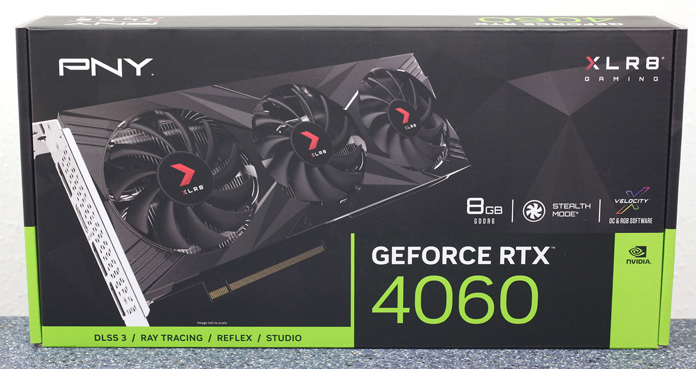
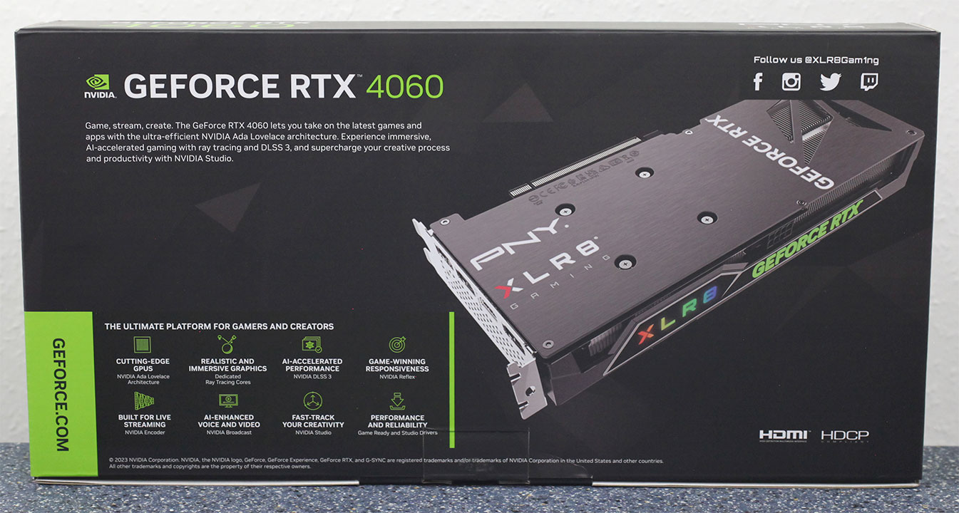
PNY GeForce RTX 4060 XLR8 Review
(8 Comments) »Introduction
PNY's GeForce RTX 4060 XLR8 is a premium custom-design graphics card based on NVIDIA's latest mid-range GPU that's bound to sell in heaps. The XLR8 (pronounced: accelerate) tops the RTX 4060 with a large cooling solution designed to keep fan noise low when gaming; and while it sticks to NVIDIA-reference clock-speeds, you have headroom to overclock the card on your own. PNY is trying to undercut other premium custom-design RTX 4060 cards by offering their card at close-to-MSRP pricing, while giving you some of the features you expect from premium custom-designs.
The new GeForce RTX 4060 targets the vast majority of gamers that still play at 1080p resolution. It succeeds a long line of bestselling graphics cards by NVIDIA, including the RTX 3060, RTX 2060, and the GTX 1060, which have topped Steam Hardware Survey charts for popularity. Full HD remains a reasonable resolution for PC gamers to experience the eye-candy of today's AAA games, and so NVIDIA's job with the RTX 4060 is to provide them with a card that they can max out their games at 1080p, including with ray tracing, and take advantage of next-generation features.

The GeForce RTX 4060 is firmly a new-generation graphics card that's based on the Ada Lovelace graphics architecture. It has two big things going for it that make it preferable to previous-generation graphics cards. Firstly, it gets the full RTX 40-series feature-set, which means support for DLSS 3 Frame Generation, something that nearly doubles frame-rates on supported games by drawing entire frames using AI, and without involving the graphics rendering machinery; and secondly, since the RTX 4060 is manufactured on the 5 nm foundry process, it comes with the lowest typical gaming power figures for any graphics card from this generation, rated at just 115 W.
The GeForce RTX 4060 maxes out the 5 nm AD107 silicon that it is based on. In a surprising move, NVIDIA is using its smallest ASIC from this generation to make the RTX 4060, while its sibling, the RTX 4060 Ti, nearly maxes out the larger AD106 silicon. Armed with 24 streaming multiprocessors (SM), the RTX 4060 gets 3,072 CUDA cores, 96 Tensor cores, 24 RT cores, and 96 TMUs. The AD107 features 48 ROPs, and the same 128-bit GDDR6 memory interface as the AD106, which on the RTX 4060 is wired to 8 GB of video memory. Generationally, this is a 50% reduction in memory size and bus width, but NVIDIA assures us that the 8 times larger on-die cache makes up for it, by reducing video memory round-trips by 40% to 60% in NVIDIA's testing.
PNY is pricing the GeForce RTX 4060 XLR8 OC at a reasonable $320, or just $20 more than the NVIDIA MSRP. For the premium, you're offered a more capable cooling solution that's designed to run quieter than most MSRP cards, although the card does not come with any factory overclock. The GPU runs at the NVIDIA reference 2460 MHz, and the memory is untouched at 17 Gbps. It will be interesting to find out what the extra $20 is worth, having seen some of the MSRP cards that even offer overclocked speeds.
Short 10-Minute Video Comparing 10x RTX 4060
Our goal with the videos is to create short summaries, not go into all the details and test results, which can be found in our written reviews.
| Price | Cores | ROPs | Core Clock | Boost Clock | Memory Clock | GPU | Transistors | Memory | |
|---|---|---|---|---|---|---|---|---|---|
| RX 6500 XT | $150 | 1024 | 32 | 2685 MHz | 2825 MHz | 2248 MHz | Navi 24 | 5400M | 4 GB, GDDR6, 64-bit |
| RTX 2060 | $170 | 1920 | 48 | 1365 MHz | 1680 MHz | 1750 MHz | TU106 | 10800M | 6 GB, GDDR6, 192-bit |
| RX 5700 XT | $150 | 2560 | 64 | 1605 MHz | 1755 MHz | 1750 MHz | Navi 10 | 10300M | 8 GB, GDDR6, 256-bit |
| RTX 3050 | $210 | 2560 | 32 | 1552 MHz | 1777 MHz | 1750 MHz | GA106 | 12000M | 8 GB, GDDR6, 128-bit |
| RTX 2070 | $210 | 2304 | 64 | 1410 MHz | 1620 MHz | 1750 MHz | TU106 | 10800M | 8 GB, GDDR6, 256-bit |
| Arc A750 | $240 | 3584 | 112 | 2050 MHz | N/A | 2000 MHz | ACM-G10 | 21700M | 8 GB, GDDR6, 256-bit |
| RX 6600 | $170 | 1792 | 64 | 2044 MHz | 2491 MHz | 1750 MHz | Navi 23 | 11060M | 8 GB, GDDR6, 128-bit |
| RX 6600 XT | $210 | 2048 | 64 | 2359 MHz | 2589 MHz | 2000 MHz | Navi 23 | 11060M | 8 GB, GDDR6, 128-bit |
| RTX 3060 | $260 | 3584 | 48 | 1320 MHz | 1777 MHz | 1875 MHz | GA106 | 12000M | 12 GB, GDDR6, 192-bit |
| RX 7600 | $250 | 2048 | 64 | 2250 MHz | 2625 MHz | 2250 MHz | Navi 33 | 13300M | 8 GB, GDDR6, 128-bit |
| RTX 4060 | $300 | 3072 | 48 | 1830 MHz | 2460 MHz | 2125 MHz | AD107 | 18900M | 8 GB, GDDR6, 128-bit |
| PNY RTX 4060 XLR8 | $320 | 3072 | 48 | 1830 MHz | 2460 MHz | 2125 MHz | AD107 | 18900M | 8 GB, GDDR6, 128-bit |
| Arc A770 | $290 | 4096 | 128 | 2100 MHz | N/A | 2187 MHz | ACM-G10 | 21700M | 16 GB, GDDR6, 256-bit |
| RTX 2080 | $240 | 2944 | 64 | 1515 MHz | 1710 MHz | 1750 MHz | TU104 | 13600M | 8 GB, GDDR6, 256-bit |
| RTX 3060 Ti | $300 | 4864 | 80 | 1410 MHz | 1665 MHz | 1750 MHz | GA104 | 17400M | 8 GB, GDDR6, 256-bit |
| RTX 4060 Ti | $380 | 4352 | 48 | 2310 MHz | 2535 MHz | 2250 MHz | AD106 | 22900M | 8 GB, GDDR6, 128-bit |
| RX 6700 XT | $310 | 2560 | 64 | 2424 MHz | 2581 MHz | 2000 MHz | Navi 22 | 17200M | 12 GB, GDDR6, 192-bit |
| RTX 2080 Ti | $380 | 4352 | 88 | 1350 MHz | 1545 MHz | 1750 MHz | TU102 | 18600M | 11 GB, GDDR6, 352-bit |
| RTX 3070 | $320 | 5888 | 96 | 1500 MHz | 1725 MHz | 1750 MHz | GA104 | 17400M | 8 GB, GDDR6, 256-bit |
| RTX 3070 Ti | $400 | 6144 | 96 | 1575 MHz | 1770 MHz | 1188 MHz | GA104 | 17400M | 8 GB, GDDR6X, 256-bit |
| RX 6800 | $430 | 3840 | 96 | 1815 MHz | 2105 MHz | 2000 MHz | Navi 21 | 26800M | 16 GB, GDDR6, 256-bit |
Architecture
The Ada graphics architecture heralds the third generation of the NVIDIA RTX technology, an effort toward increasing the realism of game visuals by leveraging real-time ray tracing, without the enormous amount of compute power required to draw purely ray-traced 3D graphics. This is done by blending conventional raster graphics with ray traced elements such as reflections, lighting, and global illumination, to name a few. The 3rd generation of RTX introduces the new higher IPC "Ada" CUDA core, 3rd generation RT core, 4th generation Tensor core, and the new Optical Flow Processor, a component that plays a key role in generating new frames without involving the GPU's main graphics rendering pipeline.


The GeForce Ada graphics architecture driving the RTX 4060 leverages the TSMC 5 nm EUV foundry process to increase transistor counts. At the heart of this GPU is the new AD107 silicon, with a transistor count of 18.9 billion, which is almost 60% higher than that of the previous-generation GA106, and about 9% more than the GA104. The GPU features a generationally narrower PCI-Express 4.0 x8 host interface, and a 128-bit wide GDDR6 memory interface. This is causing some controversy, and we'll present NVIDIA's explanation below. The Optical Flow Accelerator (OFA) is an independent top-level component. For the RTX 4060, the chip features one 8th Gen NVENC and one 5th Gen NVDEC unit, including hardware-acceleration for the AV1 format.
The essential component hierarchy is similar to past generations of NVIDIA GPUs. The AD107 silicon features 3 Graphics Processing Clusters (GPCs), each of these has all the SIMD and graphics rendering machinery, and is a small GPU in its own right. Each GPC shares a raster engine (geometry processing components) and two ROP partitions (each with eight ROP units). The GPC of the AD107 contains four Texture Processing Clusters (TPCs), the main number-crunching machinery. Each of these has two Streaming Multiprocessors (SM), and a Polymorph unit. Each SM contains 128 CUDA cores across four partitions. Half of these CUDA cores are pure-FP32; while the other half is capable of FP32 or INT32. The SM retains concurrent FP32+INT32 math processing capability. The SM also contains a 3rd generation RT core, four 4th generation Tensor cores, some cache memory, and four TMUs. There are 8 SM per GPC, so 1,024 CUDA cores, 32 Tensor cores, and 8 RT cores; per GPC. There are three such GPCs, which add up to 3,072 CUDA cores, 96 TMUs, 96 Tensor Cores, and 24 RT cores. There are 48 ROPs on the silicon. The AD107 features a 24 MB L2 cache, which is smaller than the 32 MB on the AD106 powering the RTX 4060 Ti.
3rd Gen RT Core and Ray Tracing
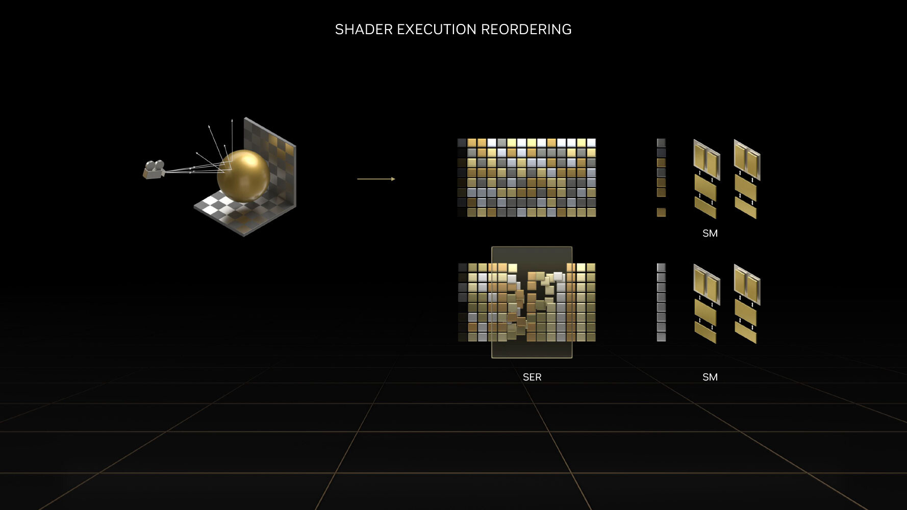
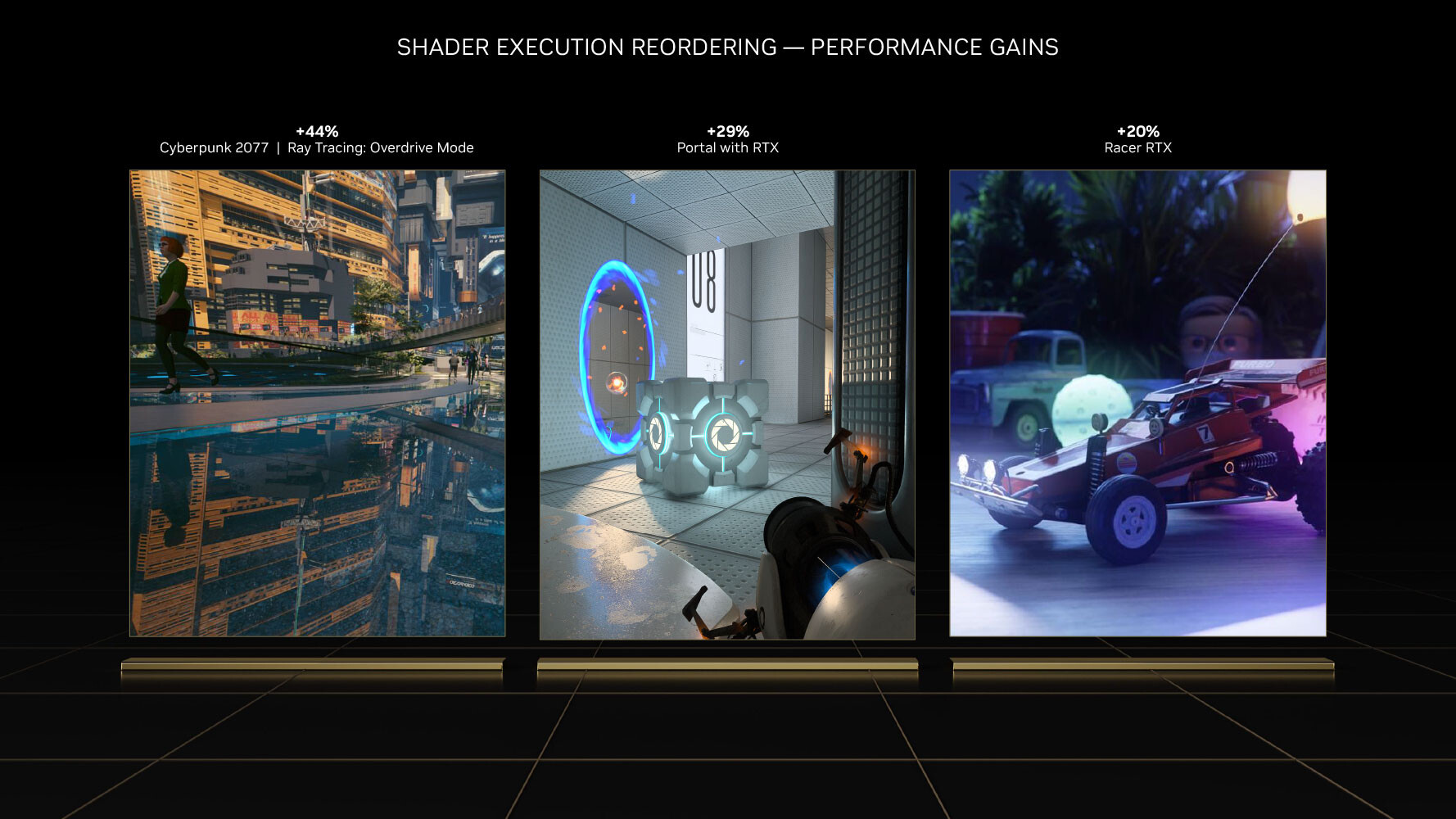
The 3rd generation RT core accelerates the most math-intensive aspects of real-time ray tracing, including BVH traversal. Displaced micro-mesh engine is a revolutionary feature introduced with the new 3rd generation RT core. Just as mesh shaders and tessellation have had a profound impact on improving performance with complex raster geometry, allowing game developers to significantly increase geometric complexity; DMMs is a method to reduce the complexity of the bounding-volume hierarchy (BVH) data-structure, which is used to determine where a ray hits geometry. Previously, the BVH had to capture even the smallest details to properly determine the intersection point. Ada's ray tracing architecture also receives a major performance uplift from Shader Execution Reordering (SER), a software-defined feature that requires awareness from game-engines, to help the GPU reorganize and optimize worker threads associated with ray tracing.
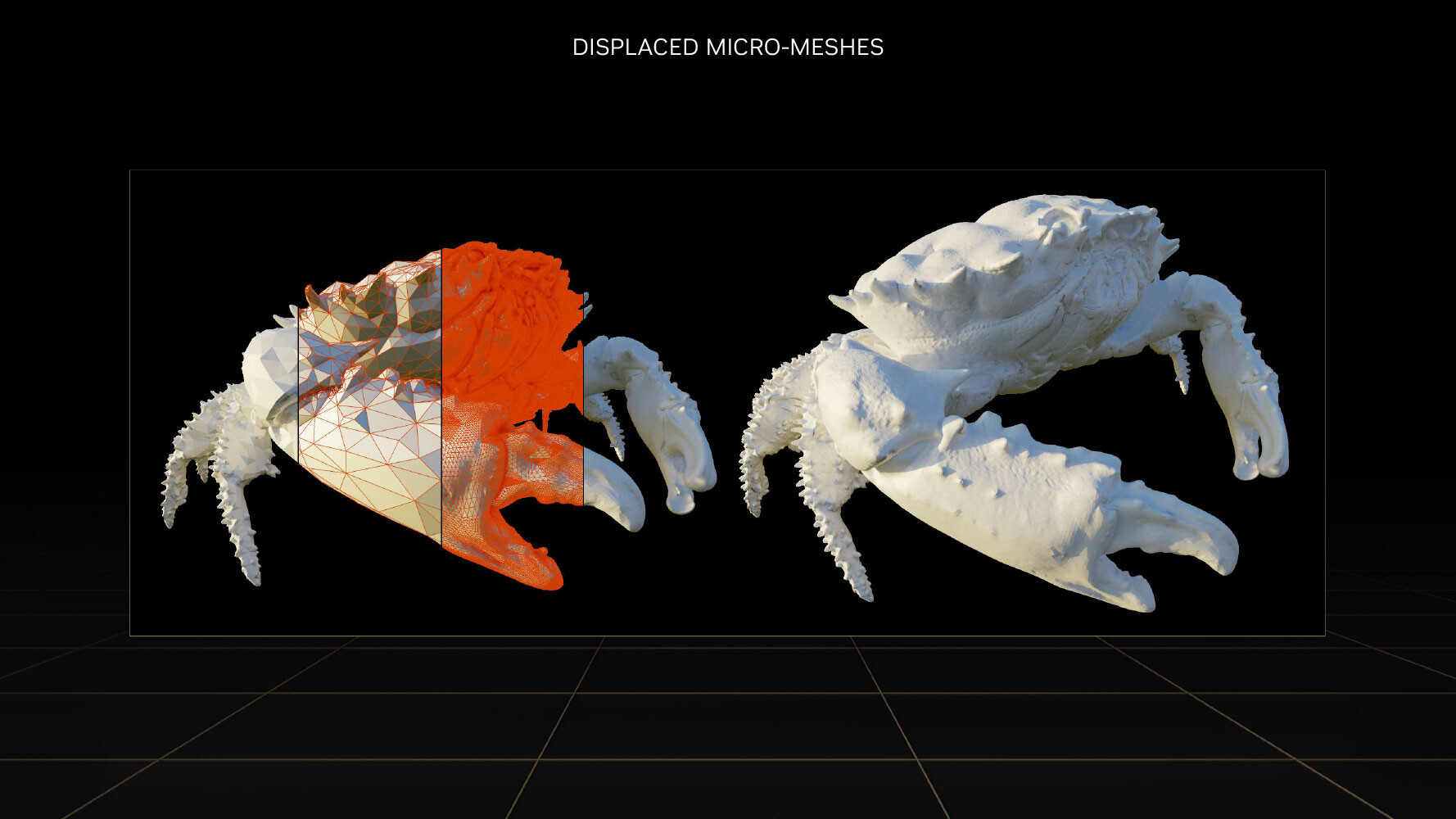

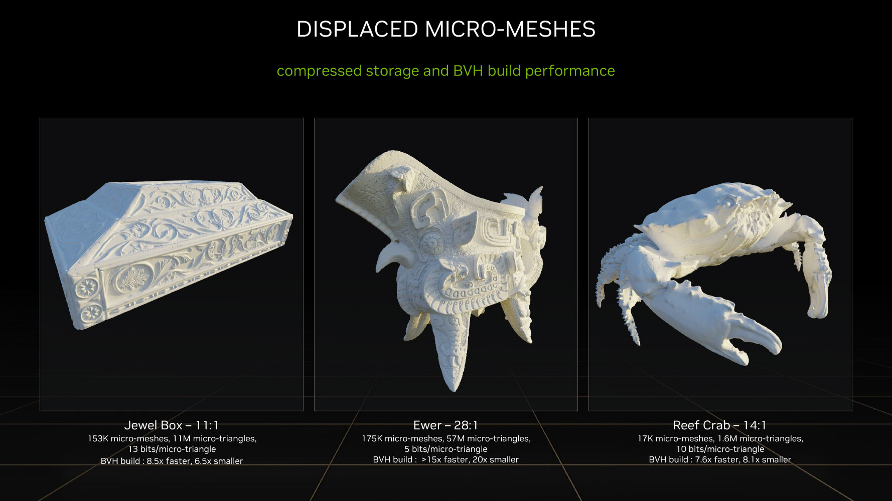
The BVH now needn't have data for every single triangle on an object, but can represent objects with complex geometry as a coarse mesh of base triangles, which greatly simplifies the BVH data structure. A simpler BVH means less memory consumed and helps to greatly reduce ray tracing CPU load, because the CPU only has to generate a smaller structure. With older "Ampere" and "Turing" RT cores, each triangle on an object had to be sampled at high overhead, so the RT core could precisely calculate ray intersection for each triangle. With Ada, the simpler BVH, plus the displacement maps can be sent to the RT core, which is now able to figure out the exact hit point on its own. NVIDIA has seen 11:1 to 28:1 compression in total triangle counts. This reduces BVH compile times by 7.6x to over 15x, in comparison to the older RT core; and reducing its storage footprint by anywhere between 6.5 to 20 times. DMMs could reduce disk- and memory bandwidth utilization, utilization of the PCIe bus, as well as reduce CPU utilization. NVIDIA worked with Simplygon and Adobe to add DMM support for their tool chains.
Opacity Micro Meshes

Opacity Micro Meshes (OMM) is a new feature introduced with Ada to improve rasterization performance, particularly with objects that have alpha (transparency data). Most low-priority objects in a 3D scene, such as leaves on a tree, are essentially rectangles with textures on the leaves where the transparency (alpha) creates the shape of the leaf. RT cores have a hard time intersecting rays with such objects, because they're not really in the shape that they appear (they're really just rectangles with textures that give you the illusion of shape). Previous-generation RT cores had to have multiple interactions with the rendering stage to figure out the shape of a transparent object, because they couldn't test for alpha by themselves.


This has been solved by using OMMs. Just as DMMs simplify geometry by creating meshes of micro-triangles; OMMs create meshes of rectangular textures that align with parts of the texture that aren't alpha, so the RT core has a better understanding of the geometry of the object, and can correctly calculate ray intersections. This has a significant performance impact on shading performance in non-RT applications, too. Practical applications of OMMs aren't just low-priority objects such as vegetation, but also smoke-sprites and localized fog. Traditionally there was a lot of overdraw for such effects, because they layered multiple textures on top of each other, that all had to be fully processed by the shaders. Now only the non-opaque pixels get executed—OMMs provide a 30 percent speedup with graphics buffer fill-rates, and a 10 percent impact on frame-rates.
DLSS 3 Frame Generation
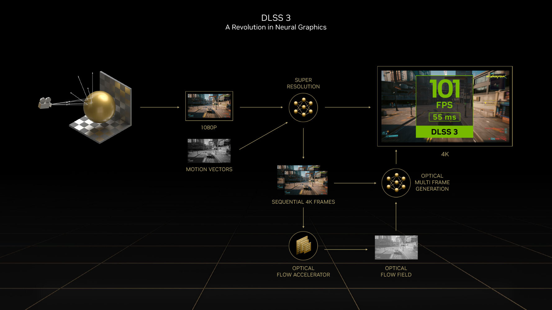

DLSS 3 introduces a revolutionary new feature that promises a doubling in frame-rate at comparable quality, it's called AI frame-generation. Building on DLSS 2 and its AI super-resolution (scaling up a lower-resolution frame to native resolution with minimal quality loss); DLSS 3 can generate entire frames simply using AI, without involving the graphics rendering pipeline, it's also possible to enable frame generation at native resolution without upscaling. Later in the article, we will show you DLSS 3 in action.
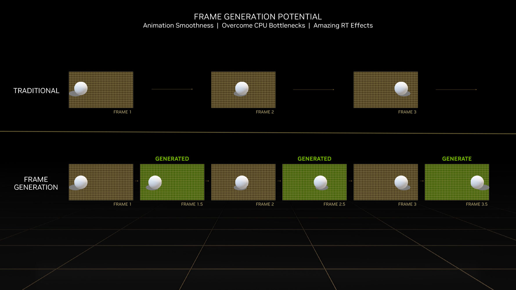
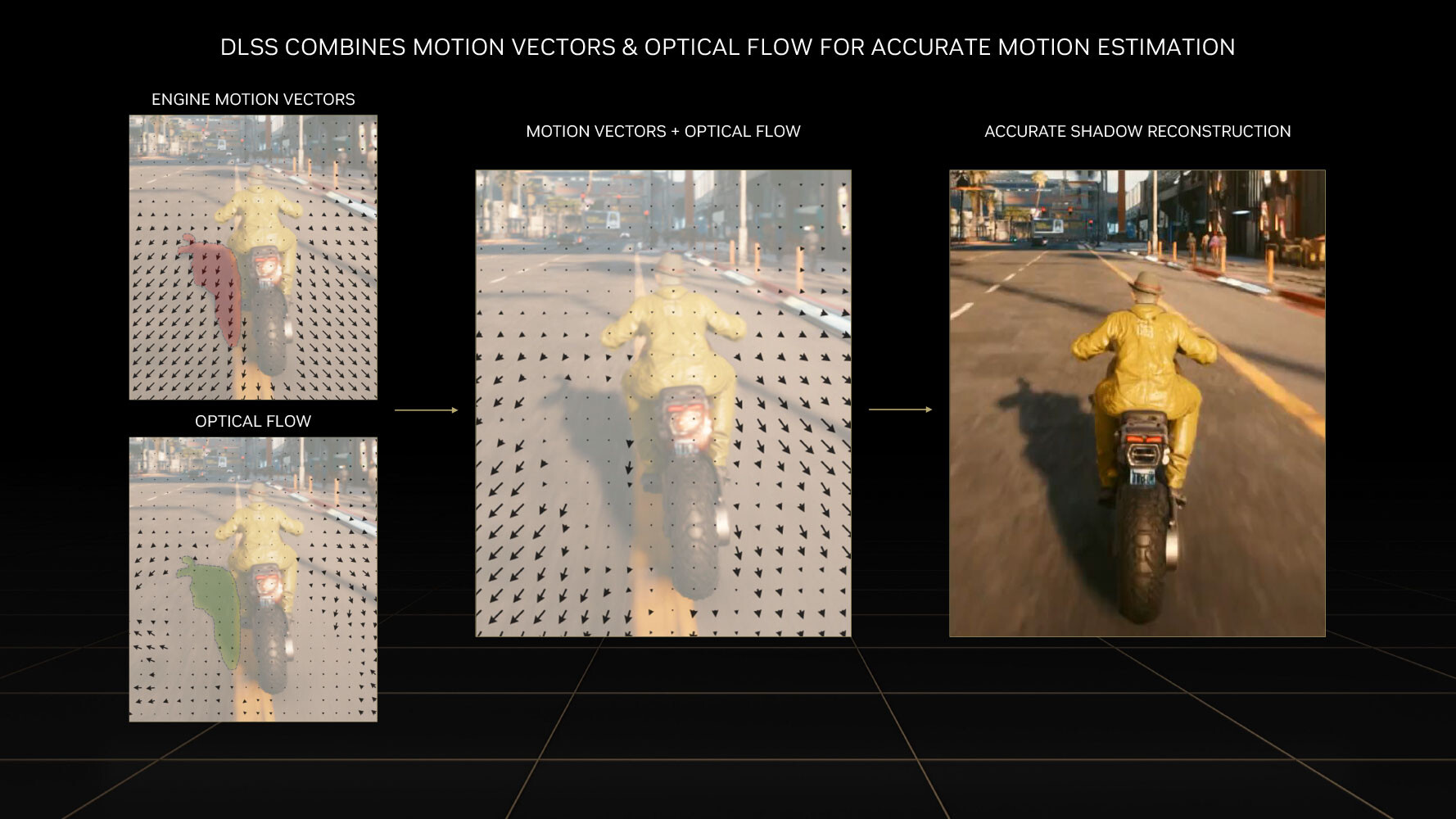
Every alternating frame with DLSS 3 is hence AI-generated, without being a replica of the previous rendered frame. This is possible only on the Ada graphics architecture, because of a hardware component called the optical flow accelerator (OFA), which assists in predicting what the next frame could look like, by creating what NVIDIA calls an optical flow-field. OFA ensures that the DLSS 3 algorithm isn't confused by static objects in a rapidly-changing 3D scene (such as a race sim). The process heavily relies on the performance uplift introduced by the FP8 math format of the 4th generation Tensor core. A third key ingredient of DLSS 3 is Reflex. By reducing the rendering queue to zero, Reflex plays a vital role in ensuring that latency with DLSS 3 enabled is at an acceptable level. A combination of OFA and the 4th Gen Tensor core is why the Ada architecture is required to use DLSS 3, and why it won't work on older architectures.
Ada Rebalanced Memory Subsystem

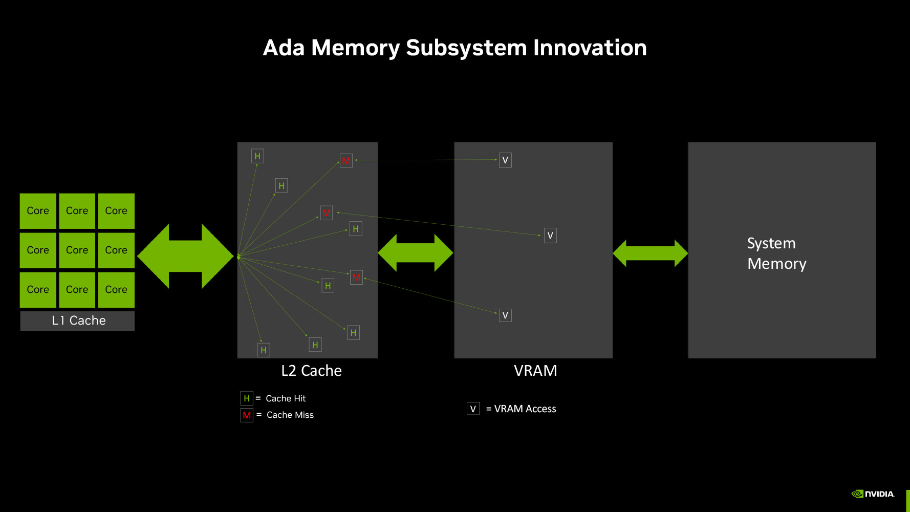
The previous-generation GeForce RTX 3060 featured a 192-bit wide GDDR6 memory interface driving its 12 GB of 14 Gbps-rated GDDR6 memory, which has caused some controversy with the RTX 4060 using a narrower 128-bit wide memory interface to drive 8 GB of 17 Gbps memory. With the new Ada Lovelace graphics architecture, NVIDIA has tried to re-balance the memory sub-system such that there's dependence on larger on-die caches, allowing NVIDIA to narrow down the GPU's GDDR6 memory interface. The obvious benefit of this to NVIDIA is reduced costs, let's make no mistake about it, but NVIDIA maintains that this isn't a big problem for the GPU.
The last-level cache, or L2 cache, of NVIDIA Ada GPUs is anywhere between 8-10 times larger than the ones on the previous-generation Ampere GPUs. The AD107 silicon powering the RTX 4060 has a 24 MB L2 cache, compared to the 2 MB of the GA107 silicon powering the RTX 3050, and 3 MB of the GA106 powering the RTX 3060. NVIDIA illustrated an example of how the larger on-die LLC reduces video memory pressure (trips to GDDR6) by anywhere between 40% to 60% on the same GPU, by soaking up a larger number of memory access requests by the shaders.
The L2 cache is unified victim cache to the GPU's various GPCs and their local TPCs. Data that isn't hot enough (frequently accessed enough) to be resident on the small L1 caches of the SM, is ejected to the L2 cache, and depending on its heat, pushed to the GDDR6 video memory. The L2 cache is an order of magnitude faster than than video memory in terms of latency, and so having frequently-accessed data reside there offers a considerable benefit.
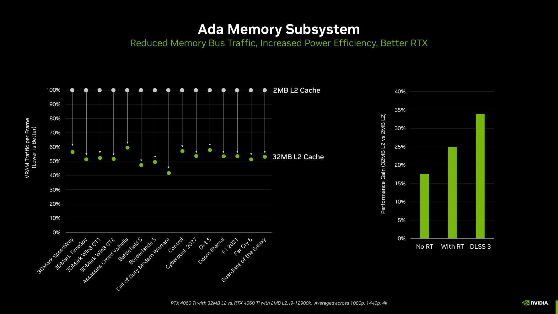
As we mentioned earlier from NVIDIA's claims, this re-balancing of the memory sub-system between the on-die LLC and video memory lowers the GPU's access to the latter by as much as 60%, which means the GPU can make do with a narrower 128-bit wide GDDR6 memory bus. NVIDIA has used generationally faster 17 Gbps memory chips in the RTX 4060. NVIDIA developed a new means of presenting the memory bandwidth that takes into account the contribution of the L2 cache, its hit-rate, and the consequent reduction in video memory traffic. While the memory bandwidth of the RTX 4060 is 272 GB/s, NVIDIA claims that its "effective bandwidth" is 453 GB/s. It's interesting to point out that NVIDIA has used "effective bandwidth" figures in the past to highlight its lossless memory compression technologies, but has never been this vocal about it.
Packaging
Our Patreon Silver Supporters can read articles in single-page format.
May 4th, 2025 20:05 EDT
change timezone
Latest GPU Drivers
New Forum Posts
- 12600KF high latency (24)
- is it possible to buy a sata to propietary dell pata adapter? (0)
- Half Life 3 soon ? (10)
- Best USB 3 hub chipsets (17)
- The TPU Darkroom - Digital SLR and Photography Club (4085)
- RX 9000 series GPU Owners Club (634)
- 245KF e-cores running full clock after update (5)
- Are the 8 GB cards worth it? (835)
- Vertical mice in gaming (11)
- The TPU UK Clubhouse (26194)
Popular Reviews
- Clair Obscur: Expedition 33 Performance Benchmark Review - 33 GPUs Tested
- ASUS ROG Maximus Z890 Hero Review
- ASUS Radeon RX 9070 XT TUF OC Review
- Montech HS02 PRO Review
- NVIDIA GeForce RTX 5060 Ti 8 GB Review - So Many Compromises
- ASUS GeForce RTX 5090 Astral Liquid OC Review - The Most Expensive GPU I've Ever Tested
- Seasonic Vertex GX 850 W Review
- Upcoming Hardware Launches 2025 (Updated Apr 2025)
- ASRock Radeon RX 9070 XT Taichi OC Review - Excellent Cooling
- Sapphire Radeon RX 9070 XT Nitro+ Review - Beating NVIDIA
Controversial News Posts
- AMD Radeon RX 9060 XT to Roll Out 8 GB GDDR6 Edition, Despite Rumors (129)
- NVIDIA Sends MSRP Numbers to Partners: GeForce RTX 5060 Ti 8 GB at $379, RTX 5060 Ti 16 GB at $429 (128)
- NVIDIA Launches GeForce RTX 5060 Series, Beginning with RTX 5060 Ti This Week (115)
- Nintendo Confirms That Switch 2 Joy-Cons Will Not Utilize Hall Effect Stick Technology (105)
- NVIDIA PhysX and Flow Made Fully Open-Source (95)
- Sony Increases the PS5 Pricing in EMEA and ANZ by Around 25 Percent (84)
- Parts of NVIDIA GeForce RTX 50 Series GPU PCB Reach Over 100°C: Report (78)
- Intel "Bartlett Lake-S" Gaming CPU is Possible, More Hints Appear for a 12 P-Core SKU (77)