 4
4
PNY GeForce RTX 4070 Review
(4 Comments) »Introduction
PNY GeForce RTX 4070 leads the company's custom-design RTX 4070 lineup from the front. As a company, PNY has come a long way from a memory products vendor for photographers, to an OEM focusing on professional-visualization graphics cards. The company has seriously stepped up its game in the consumer graphics segment with the RTX 40-series Ada generation. The card in this review is called simply the PNY GeForce RTX 4070, there's no brand extension as such. It is intended to be sold at the NVIDIA MSRP of $600, alongside every other RTX 4070 card we are reviewing for you today. This is because NVIDIA wants to encourage its board partners to have decent custom-design cards at its baseline price, and has given the MSRP cards an exclusive review publication date. Reviews of premium factory-overclocked cards priced above the MSRP go live tomorrow (April 13), which is when all RTX 4070 cards go on sale.

The GeForce RTX 4070 Ada is designed for maxed out gameplay across all genres, at resolutions of up to 1440p with native resolution; or high refresh-rate competitive e-sports gameplay at 1080p or 1440p. 4K Ultra HD gameplay is doable if you can find the right settings (or use GeForce Experience to do so); but it isn't the recommended resolution for this card. There is plenty of inventory of previous-generation graphics cards around this price, but none of them come with new features such as Optical Flow Accelerator, dual video-acceleration, or DLSS 3—a technology that generates entire alternate frames using AI, without involving the graphics rendering machinery, to nearly double frame-rates, which should have a transformative impact on games that are optimized for the feature.
The GeForce RTX 4070 is based on the same AD104 silicon as its "Ti" compatriot that launched earlier this year. While the RTX 4070 Ti maxes out the silicon, enabling all 60 streaming multiprocessors, the RTX 4070 only gets 46, which works out to 5,888 CUDA cores, 184 Tensor cores, 46 RT cores, and 184 TMUs. The ROP count is reduced from 80 to 64, too. The memory is unchanged, though—you get 12 GB of 21 Gbps GDDR6X memory across a 192-bit memory interface, with 504 GB/s of memory bandwidth on tap, that's greater than the 448 GB/s the previous-generation RTX 3070 has. The memory bus widths may appear narrower across the RTX 40-series, spare the top RTX 4090, but this is because NVIDIA has redesigned the memory sub-system at an architectural level, with much larger on-die caches on the GPU. There's still a 50% increase in memory size over the RTX 3070.
The PNY RTX 4070, as we mentioned, features a simple, minimalist board design for those who just want an RTX 4070 at MSRP to install and begin gaming, and don't care all that much about premium features such as overclocking headroom or factory-overclocked speeds. Its compact board design, with a dual-slot cooler, should be particularly appealing to those building compact or SFF gaming PCs. You also get the convenience of a legacy 8-pin PCIe power connector—that's right, NVIDIA allowed board partners to use a single 8-pin PCIe power connector design instead of the newer 16-pin 12VHPWR. The typical graphics power (TGP) being under 200 W makes this possible, as the power configuration is rated for 225 W.
| Price | Cores | ROPs | Core Clock | Boost Clock | Memory Clock | GPU | Transistors | Memory | |
|---|---|---|---|---|---|---|---|---|---|
| Arc A770 | $290 | 4096 | 128 | 2100 MHz | N/A | 2187 MHz | ACM-G10 | 21700M | 16 GB, GDDR6, 256-bit |
| RTX 2080 | $310 | 2944 | 64 | 1515 MHz | 1710 MHz | 1750 MHz | TU104 | 13600M | 8 GB, GDDR6, 256-bit |
| RTX 3060 Ti | $320 | 4864 | 80 | 1410 MHz | 1665 MHz | 1750 MHz | GA104 | 17400M | 8 GB, GDDR6, 256-bit |
| RX 6700 XT | $320 | 2560 | 64 | 2424 MHz | 2581 MHz | 2000 MHz | Navi 22 | 17200M | 12 GB, GDDR6, 192-bit |
| RTX 2080 Ti | $420 | 4352 | 88 | 1350 MHz | 1545 MHz | 1750 MHz | TU102 | 18600M | 11 GB, GDDR6, 352-bit |
| RTX 3070 | $400 | 5888 | 96 | 1500 MHz | 1725 MHz | 1750 MHz | GA104 | 17400M | 8 GB, GDDR6, 256-bit |
| RTX 3070 Ti | $500 | 6144 | 96 | 1575 MHz | 1770 MHz | 1188 MHz | GA104 | 17400M | 8 GB, GDDR6X, 256-bit |
| RX 6800 | $450 | 3840 | 96 | 1815 MHz | 2105 MHz | 2000 MHz | Navi 21 | 26800M | 16 GB, GDDR6, 256-bit |
| RX 6800 XT | $510 | 4608 | 128 | 2015 MHz | 2250 MHz | 2000 MHz | Navi 21 | 26800M | 16 GB, GDDR6, 256-bit |
| RTX 3080 | $550 | 8704 | 96 | 1440 MHz | 1710 MHz | 1188 MHz | GA102 | 28000M | 10 GB, GDDR6X, 320-bit |
| RTX 4070 | $600 | 5888 | 64 | 1920 MHz | 2475 MHz | 1313 MHz | AD104 | 35800M | 12 GB, GDDR6X, 192-bit |
| PNY RTX 4070 | $600 | 5888 | 64 | 1920 MHz | 2475 MHz | 1313 MHz | AD104 | 35800M | 12 GB, GDDR6X, 192-bit |
| RTX 3080 Ti | $750 | 10240 | 112 | 1365 MHz | 1665 MHz | 1188 MHz | GA102 | 28000M | 12 GB, GDDR6X, 384-bit |
| RX 6900 XT | $620 | 5120 | 128 | 2015 MHz | 2250 MHz | 2000 MHz | Navi 21 | 26800M | 16 GB, GDDR6, 256-bit |
| RX 6950 XT | $680 | 5120 | 128 | 2100 MHz | 2310 MHz | 2250 MHz | Navi 21 | 26800M | 16 GB, GDDR6, 256-bit |
| RTX 3090 | $800 | 10496 | 112 | 1395 MHz | 1695 MHz | 1219 MHz | GA102 | 28000M | 24 GB, GDDR6X, 384-bit |
| RTX 4070 Ti | $800 | 7680 | 80 | 2310 MHz | 2610 MHz | 1313 MHz | AD104 | 35800M | 12 GB, GDDR6X, 192-bit |
| RX 7900 XT | $800 | 5376 | 192 | 2000 MHz | 2400 MHz | 2500 MHz | Navi 31 | 57700M | 20 GB, GDDR6, 320-bit |
| RTX 3090 Ti | $1000 | 10752 | 112 | 1560 MHz | 1950 MHz | 1313 MHz | GA102 | 28000M | 24 GB, GDDR6X, 384-bit |
| RTX 4080 | $1150 | 9728 | 112 | 2205 MHz | 2505 MHz | 1400 MHz | AD103 | 45900M | 16 GB, GDDR6X, 256-bit |
| RX 7900 XTX | $960 | 6144 | 192 | 2300 MHz | 2500 MHz | 2500 MHz | Navi 31 | 57700M | 24 GB, GDDR6, 384-bit |
| RTX 4090 | $1600 | 16384 | 176 | 2235 MHz | 2520 MHz | 1313 MHz | AD102 | 76300M | 24 GB, GDDR6X, 384-bit |
Architecture
The Ada graphics architecture heralds the third generation of the NVIDIA RTX technology, an effort toward increasing the realism of game visuals by leveraging real-time ray tracing, without the enormous amount of compute power required to draw purely ray-traced 3D graphics. This is done by blending conventional raster graphics with ray traced elements such as reflections, lighting, and global illumination, to name a few. The 3rd generation of RTX introduces the new higher IPC "Ada" CUDA core, 3rd generation RT core, 4th generation Tensor core, and the new Optical Flow Processor, a component that plays a key role in generating new frames without involving the GPU's main graphics rendering pipeline.


The GeForce Ada graphics architecture driving the RTX 4070 leverages the TSMC 5 nm EUV foundry process to increase transistor counts. At the heart of this GPU is the new AD104 silicon, which has a fairly high transistor count of 35.8 billion, which is more than double that of the previous-generation GA104. The GPU features a PCI-Express 4.0 x16 host interface, and a 192-bit wide GDDR6X memory bus, which on the RTX 4070 wires out to 12 GB of memory. The Optical Flow Accelerator (OFA) is an independent top-level component. The chip features one NVENC and one NVDEC unit.
The essential component hierarchy is similar to past generations of NVIDIA GPUs. The AD104 silicon features 5 Graphics Processing Clusters (GPCs), each of these has all the SIMD and graphics rendering machinery, and is a small GPU in its own right. Each GPC shares a raster engine (geometry processing components) and two ROP partitions (each with eight ROP units). The GPC of the AD104 contains six Texture Processing Clusters (TPCs), the main number-crunching machinery. Each of these has two Streaming Multiprocessors (SM), and a Polymorph unit. Each SM contains 128 CUDA cores across four partitions. Half of these CUDA cores are pure-FP32; while the other half is capable of FP32 or INT32. The SM retains concurrent FP32+INT32 math processing capability. The SM also contains a 3rd generation RT core, four 4th generation Tensor cores, some cache memory, and four TMUs. There are 12 SM per GPC, so 1,536 CUDA cores, 48 Tensor cores, and 12 RT cores; per GPC. There are five such GPCs, which add up to 7,680 CUDA cores, 240 TMUs, 240 Tensor Cores, and 60 RT cores. Each GPC contributes 16 ROPs, so there are 80 ROPs on the silicon. The RTX 4070 is carved out of the AD104 by disabling an entire GPC worth 6 TPCs, and an additional TPC from one of the remaining GPCs. This yields 5,888 CUDA cores, 184 Tensor cores, 46 RT cores, and 184 TMUs. The ROP count has been reduced from 80 to 64. The on-die L2 cache sees a slight reduction, too, which is now down to 36 MB from the 48 MB present.


The 3rd generation RT core accelerates the most math-intensive aspects of real-time ray tracing, including BVH traversal. Displaced micro-mesh engine is a revolutionary feature introduced with the new 3rd generation RT core. Just as mesh shaders and tessellation have had a profound impact on improving performance with complex raster geometry, allowing game developers to significantly increase geometric complexity; DMM is a method to reduce the complexity of the bounding-volume hierarchy (BVH) data-structure, which is used to determine where a ray hits geometry. Previously, the BVH had to capture even the smallest details to properly determine the intersection point. Ada's ray tracing architecture also receives a major performance uplift from Shader Execution Reordering (SER), a software-defined feature that requires awareness from game-engines, to help the GPU reorganize and optimize worker threads associated with ray tracing.


The BVH now needn't have data for every single triangle on an object, but can represent objects with complex geometry as a coarse mesh of base triangles, which greatly simplifies the BVH data structure. A simpler BVH means less memory consumed and helps to greatly reduce ray tracing CPU load, because the CPU only has to generate a smaller structure. With older "Ampere" and "Turing" RT cores, each triangle on an object had to be sampled at high overhead, so the RT core could precisely calculate ray intersection for each triangle. With Ada, the simpler BVH, plus the displacement maps can be sent to the RT core, which is now able to figure out the exact hit point on its own. NVIDIA has seen 11:1 to 28:1 compression in total triangle counts. This reduces BVH compile times by 7.6x to over 15x, in comparison to the older RT core; and reducing its storage footprint by anywhere between 6.5 to 20 times. DMMs could reduce disk- and memory bandwidth utilization, utilization of the PCIe bus, as well as reduce CPU utilization. NVIDIA worked with Simplygon and Adobe to add DMM support for their tool chains.


Opacity Micro Meshes (OMM) is a new feature introduced with Ada to improve rasterization performance, particularly with objects that have alpha (transparency data). Most low-priority objects in a 3D scene, such as leaves on a tree, are essentially rectangles with textures on the leaves where the transparency (alpha) creates the shape of the leaf. RT cores have a hard time intersecting rays with such objects, because they're not really in the shape that they appear (they're really just rectangles with textures that give you the illusion of shape). Previous-generation RT cores had to have multiple interactions with the rendering stage to figure out the shape of a transparent object, because they couldn't test for alpha by themselves.


This has been solved by using OMMs. Just as DMMs simplify geometry by creating meshes of micro-triangles; OMMs create meshes of rectangular textures that align with parts of the texture that aren't alpha, so the RT core has a better understanding of the geometry of the object, and can correctly calculate ray intersections. This has a significant performance impact on shading performance in non-RT applications, too. Practical applications of OMMs aren't just low-priority objects such as vegetation, but also smoke-sprites and localized fog. Traditionally there was a lot of overdraw for such effects, because they layered multiple textures on top of each other, that all had to be fully processed by the shaders. Now only the non-opaque pixels get executed—OMMs provide a 30 percent speedup with graphics buffer fill-rates, and a 10 percent impact on frame-rates.


DLSS 3 introduces a revolutionary new feature that promises a doubling in frame-rate at comparable quality, it's called AI frame-generation. While it has all the features of DLSS 2 and its AI super-resolution (scaling up a lower-resolution frame to native resolution with minimal quality loss); DLSS 3 can generate entire frames simply using AI, without involving the graphics rendering pipeline. Later in the article, we will show you DLSS 3 in action.


Every alternating frame with DLSS 3 is hence AI-generated, without being a replica of the previous rendered frame. This is possible only on the Ada graphics architecture, because of a hardware component called the optical flow accelerator (OFA), which assists in predicting what the next frame could look like, by creating what NVIDIA calls an optical flow-field. OFA ensures that the DLSS 3 algorithm isn't confused by static objects in a rapidly-changing 3D scene (such as a race sim). The process heavily relies on the performance uplift introduced by the FP8 math format of the 4th generation Tensor core. A third key ingredient of DLSS 3 is Reflex. By reducing the rendering queue to zero, Reflex plays a vital role in ensuring that frame-times with DLSS 3 are at an acceptable level, and a render-queue doesn't confuse the upscaler. A combination of OFA and the 4th Gen Tensor core is why the Ada architecture is required to use DLSS 3, and why it won't work on older architectures.
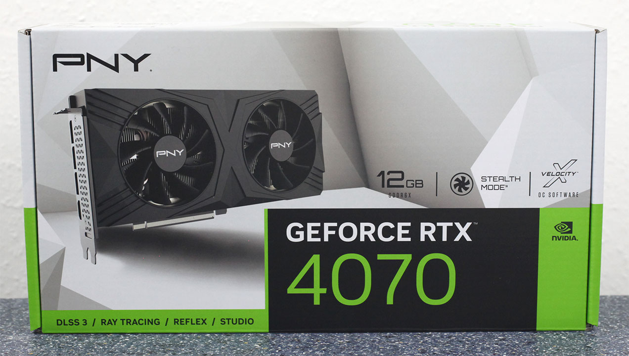
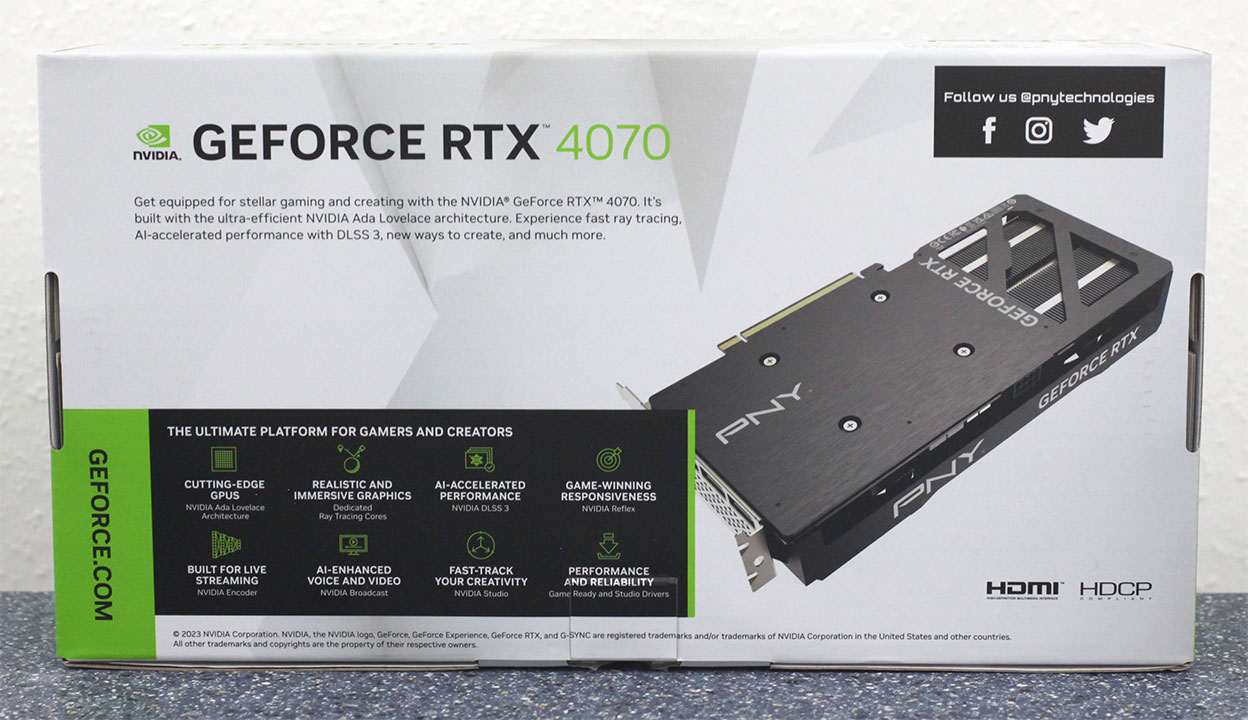
Packaging
The Card

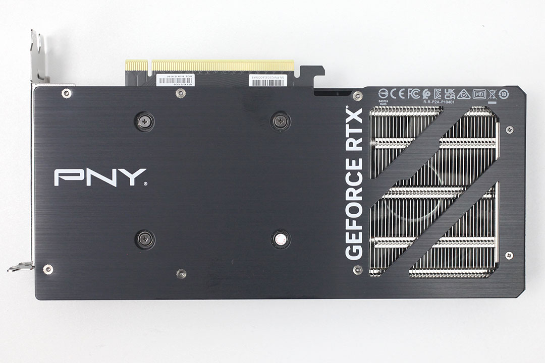
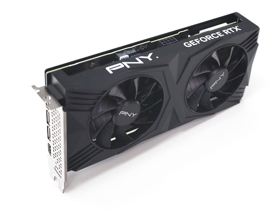
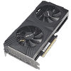
PNY's RTX 4070 use a mostly-black color theme. Thanks to the surface structure on the main cooler, light is reflected at various angles, which helps brighten up the card a bit. On the other side you'll find a metal backplate that has a cutout for air to flow through.
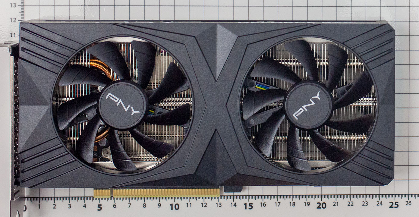
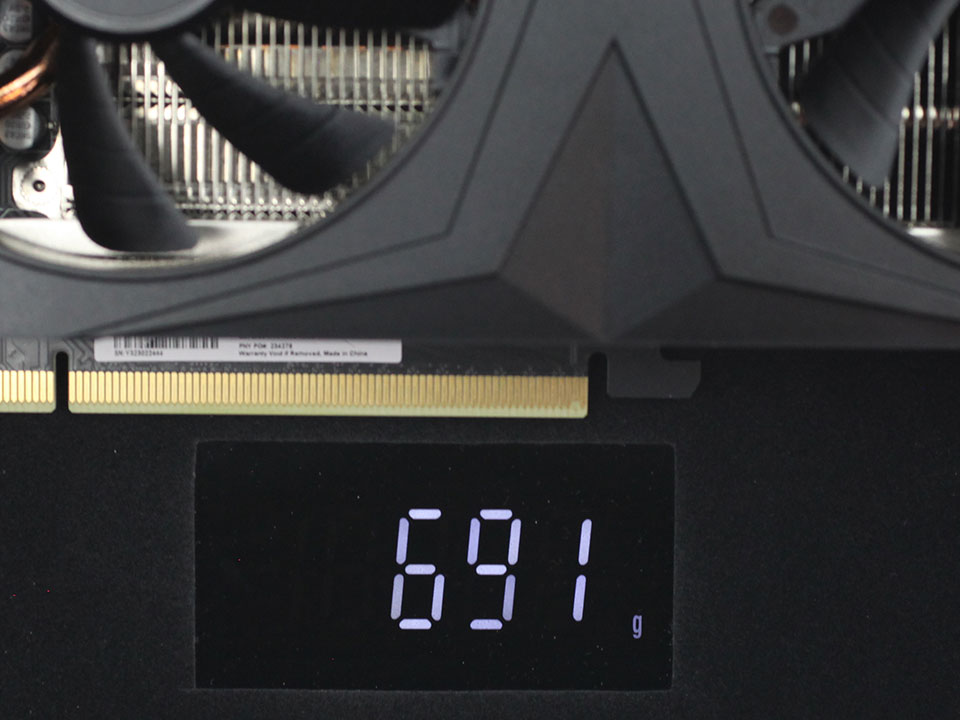
Dimensions of the card are 25 x 12 cm, and it weighs 691 g.
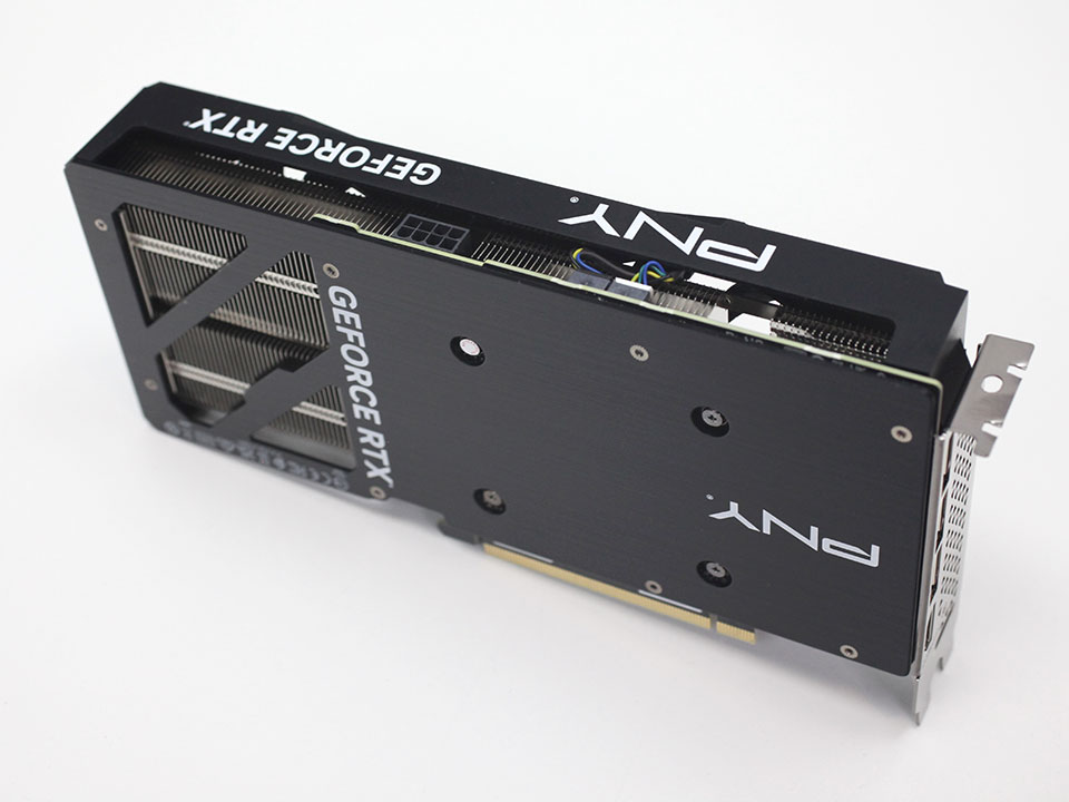
Installation requires two slots in your system.
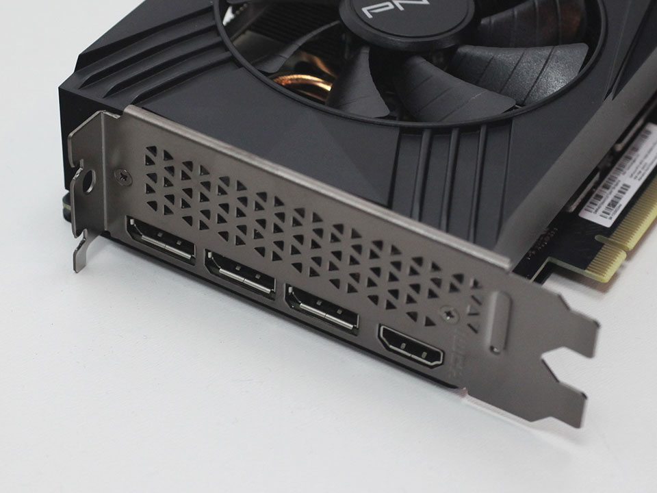
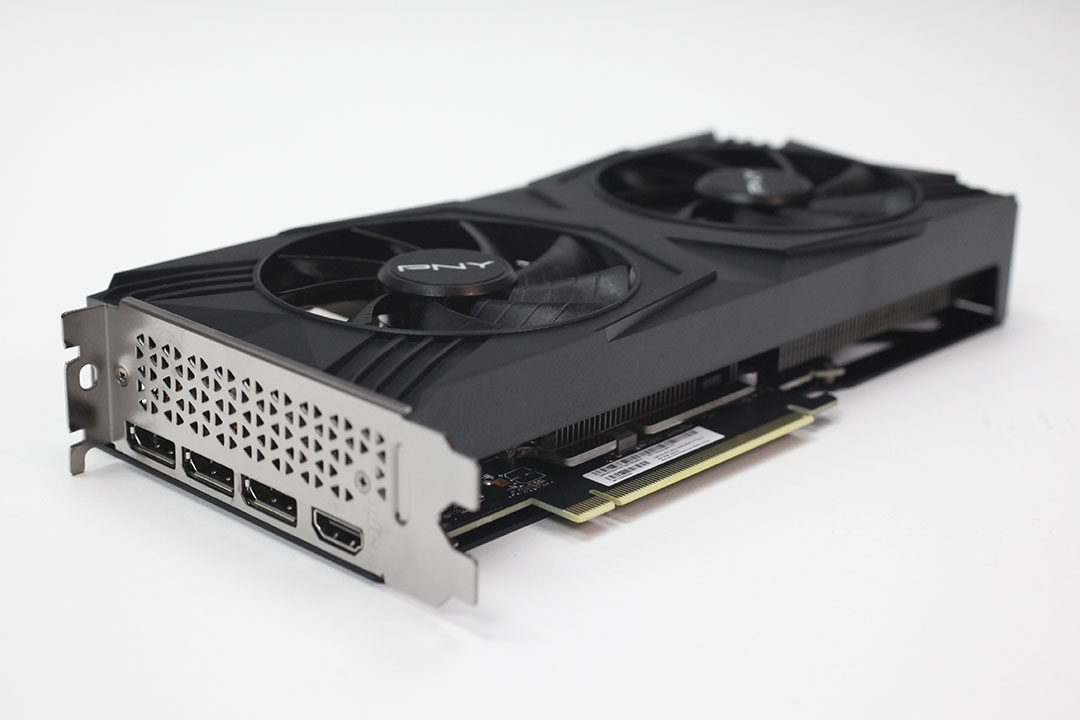
Display connectivity includes three standard DisplayPort 1.4a ports and one HDMI 2.1a (same as Ampere).
The new 8th Gen NVENC now accelerates AV1 encoding, besides HEVC. You also get an "optical flow accelerator" unit that is able to calculate intermediate frames for videos, to smooth playback. The same hardware unit is used for frame generation in DLSS 3.
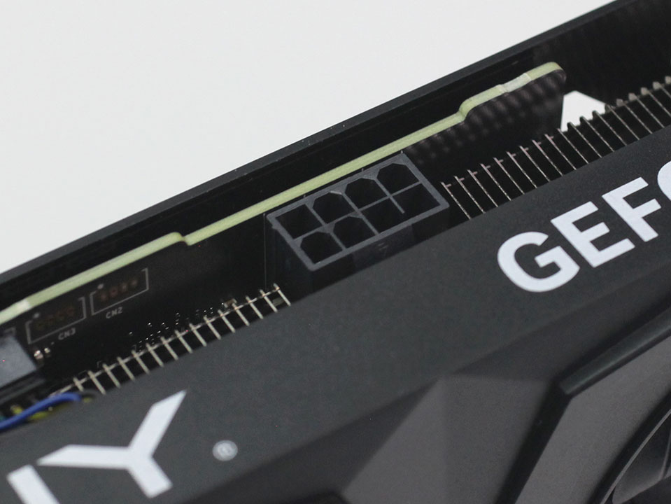
The card uses a single 8-pin power connector, which, together with the PCIe slot, is specified for up to 225 W power draw. Some other RTX 4070 cards like the NVIDIA Founders Edition come with the new 16-pin connector, but they are limited to the same power draw levels. NVIDIA has given their partners free choice on what connector they use, and I suspect the classic 8-pin is a little bit cheaper to implement.
Teardown
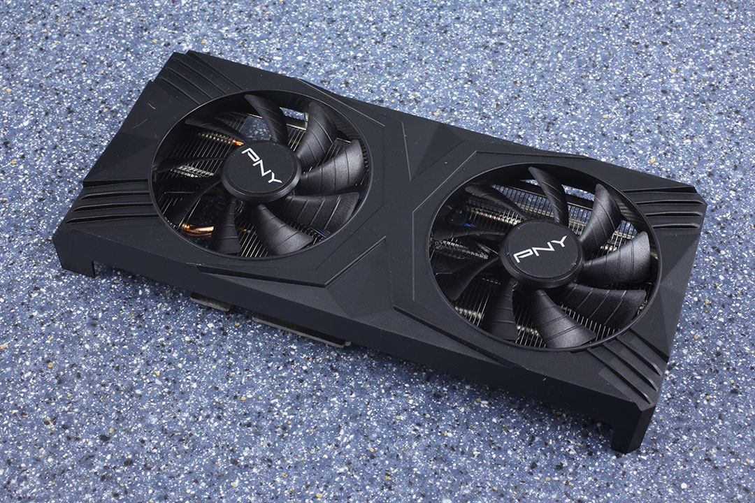
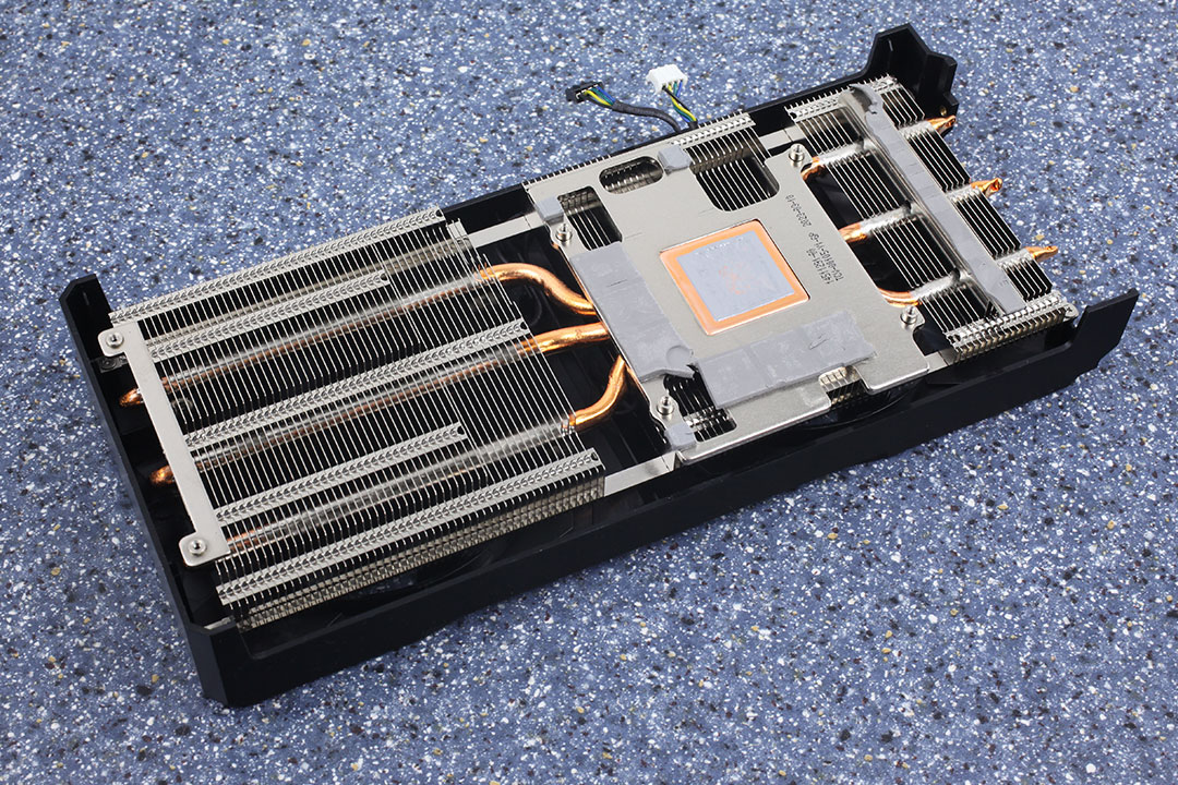
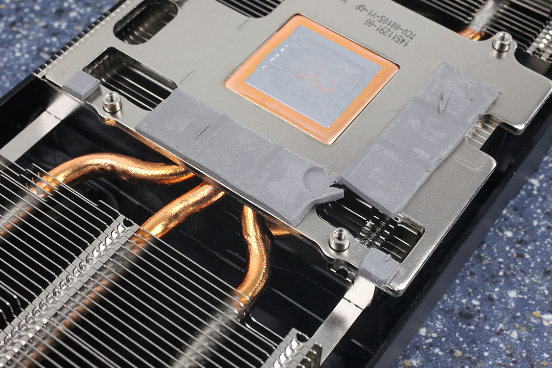
PNY's heatsink uses three heatpipes to keep the card cool. The main cooler also provides cooling for the memory chips and VRM circuitry.
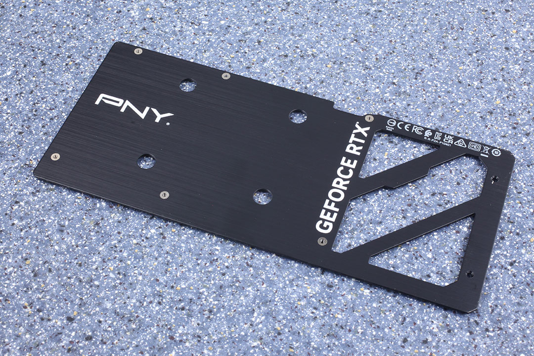
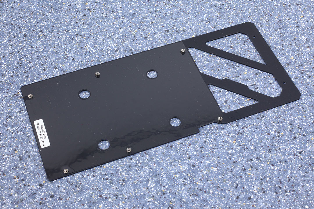
The metal backplate protects the card against damage during installation and handling.
High-resolution PCB Pictures
These pictures are for the convenience of volt modders and people who would like to see all the finer details on the PCB. Feel free to link back to us and use these in your articles, videos or forum posts.
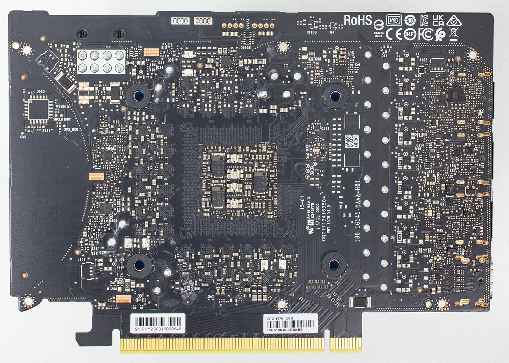
High-resolution versions are also available (front, back).
Circuit Board (PCB) Analysis
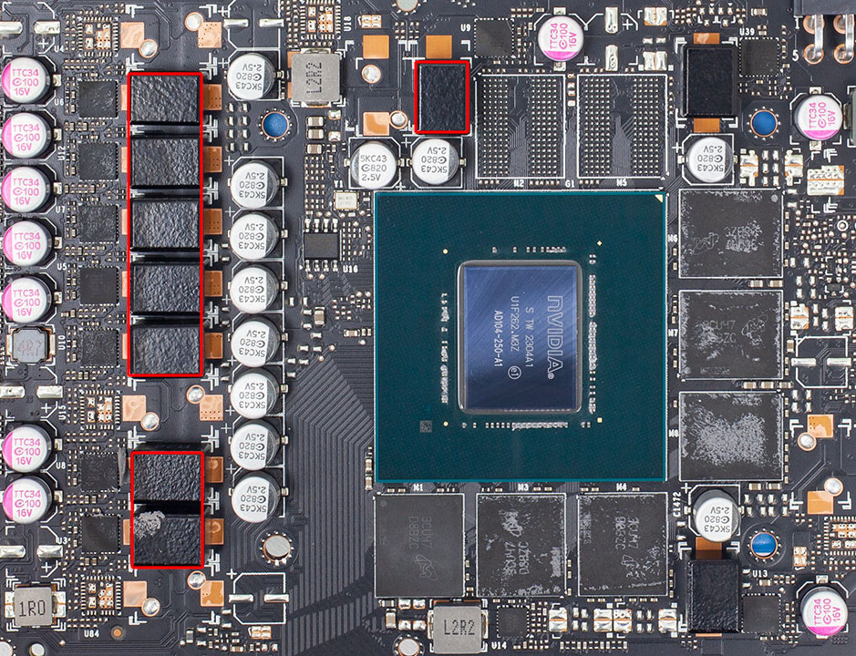
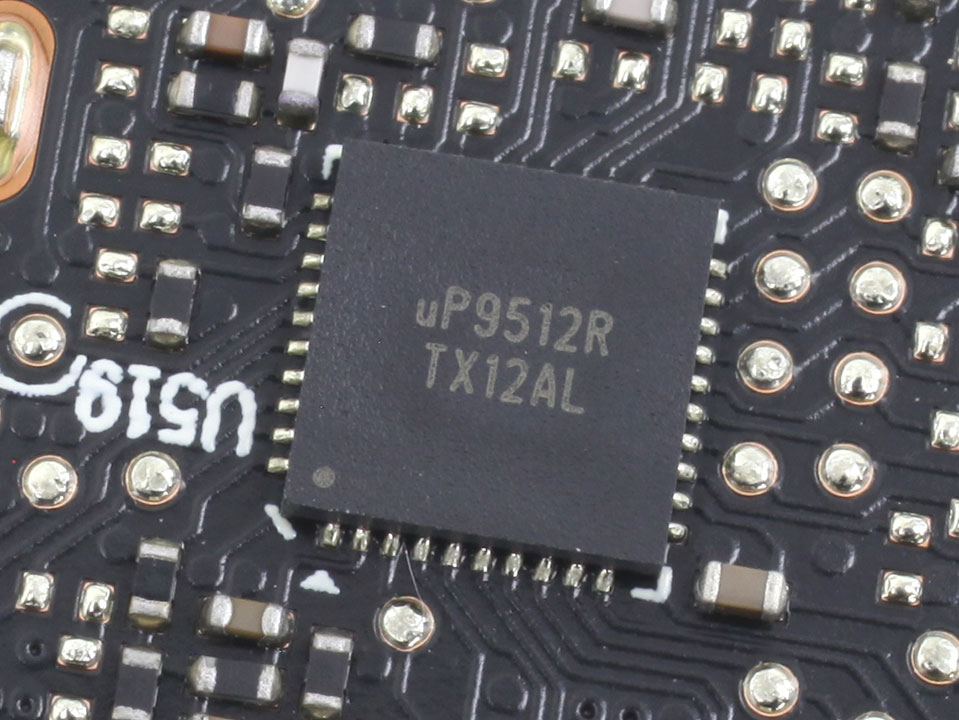
GPU voltage is a 8-phase design, managed by a uPI uP9512R controller.
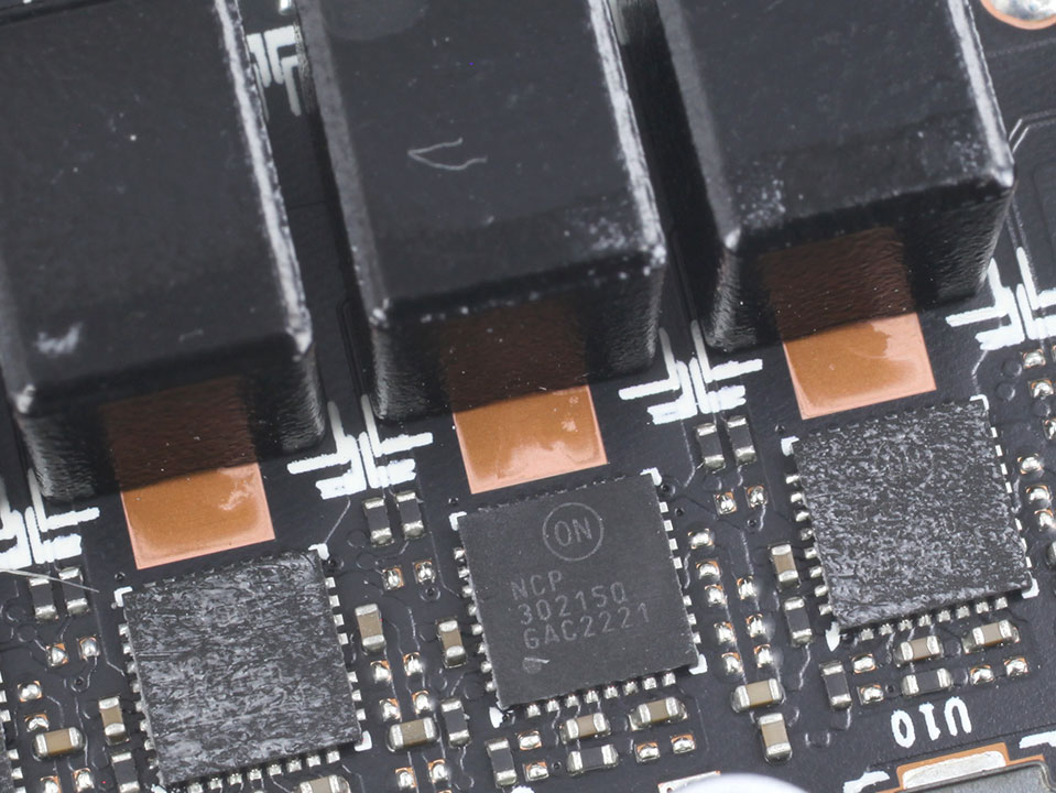
OnSemi NCP302150 DrMOS components are used for GPU voltage; they are rated for 50 A of current each.
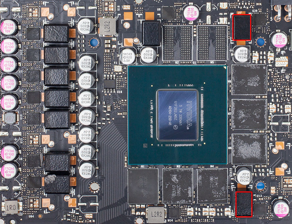
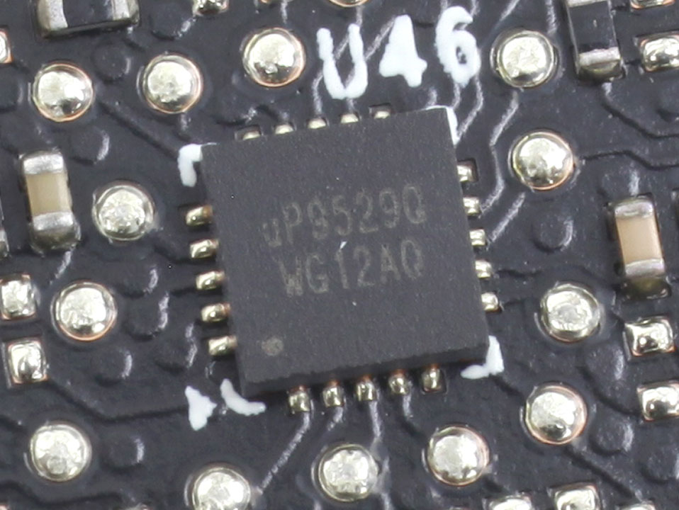
Memory voltage is a two-phase design, managed by a uPI uP9529Q controller.
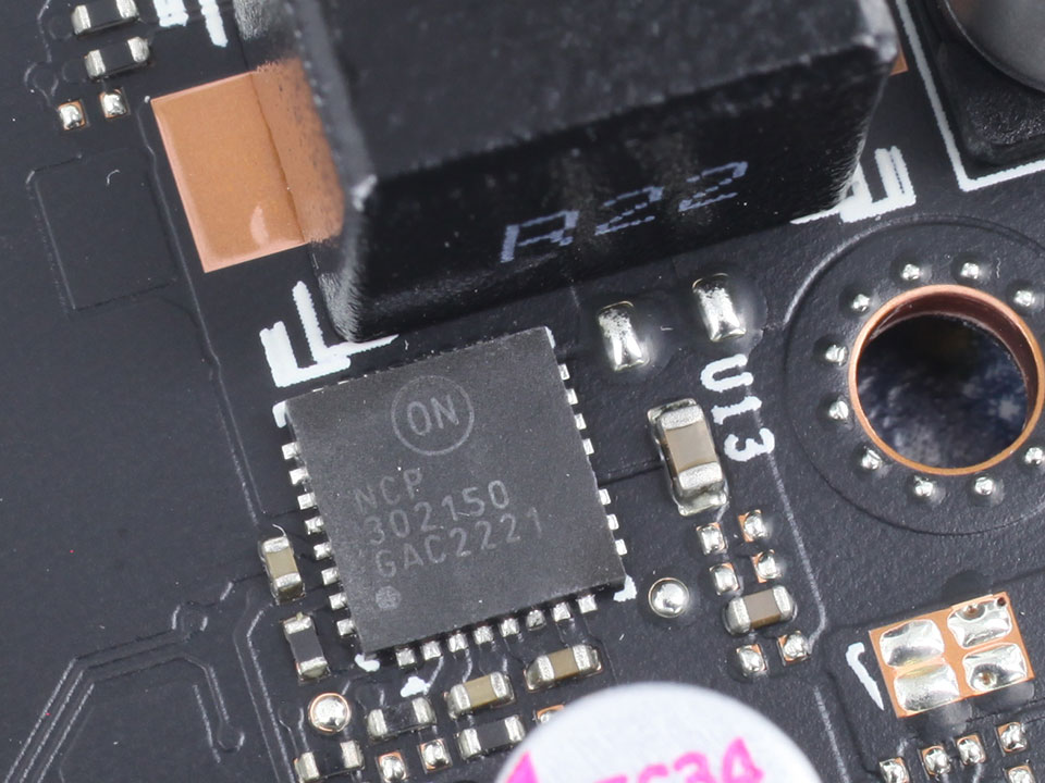
For memory, OnSemi NCP302150 DrMOS with a 50 A rating are used again.
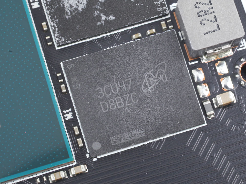
The GDDR6X memory chips are made by Micron and carry the model number D8BZC, which decodes to MT61K512M32KPA-21:U. They are specified to run at 1313 MHz (21 Gbps GDDR6 effective).
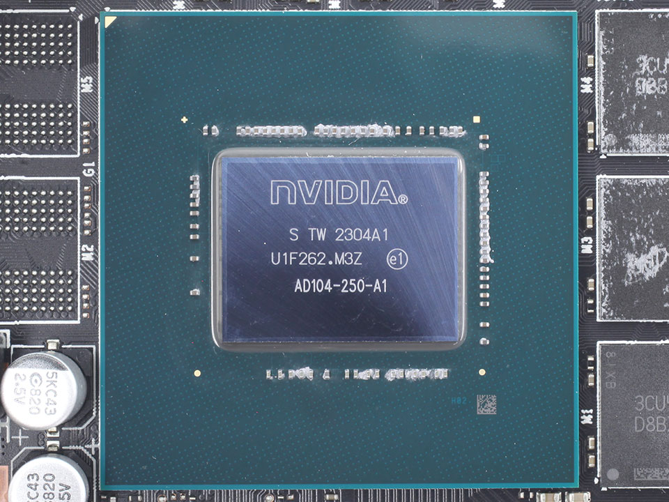
NVIDIA's AD104 graphics processor is the company's third Ada Lovelace GPU. It is built using a 5 nanometer process at TSMC Taiwan, with a transistor count of 35.8 billion and a die size of 295 mm².
Our Patreon Silver Supporters can read articles in single-page format.
Mar 11th, 2025 15:11 EDT
change timezone
Latest GPU Drivers
New Forum Posts
- GameTechBench GPU benchmark is already out! (314)
- Post your Old CDs, from back in the day thread. (43)
- 2006 Macbook Pro Modern Sleeper Project (0)
- Zen6 is almost here ? (49)
- Nvidia's GPU market share hits 90% in Q4 2024 (gets closer to full monopoly) (841)
- Avowed same FPS in every setting (1)
- TPU's Nostalgic Hardware Club (20079)
- Silent Hill Series Discussion/Speculation thread (1)
- As we live the age of game remakes, which game you would like to see to have a remake? (365)
- USB hard disk box capacity limits (16)
Popular Reviews
- Sapphire Radeon RX 9070 XT Nitro+ Review - Beating NVIDIA
- XFX Radeon RX 9070 XT Mercury OC Magnetic Air Review
- AMD Ryzen 9 9950X3D Review - Great for Gaming and Productivity
- ASUS Radeon RX 9070 TUF OC Review
- MSI MAG B850 Tomahawk Max Wi-Fi Review
- NVIDIA GeForce RTX 5070 Founders Edition Review
- Corsair Vengeance RGB CUDIMM DDR5-8800 48 GB CL42 Review
- AMD Ryzen 7 9800X3D Review - The Best Gaming Processor
- ASUS GeForce RTX 5070 Ti TUF OC Review
- MSI GeForce RTX 5070 Ti Gaming Trio OC+ Review
Controversial News Posts
- NVIDIA GeForce RTX 50 Cards Spotted with Missing ROPs, NVIDIA Confirms the Issue, Multiple Vendors Affected (513)
- AMD Radeon RX 9070 and 9070 XT Listed On Amazon - One Buyer Snags a Unit (261)
- AMD RDNA 4 and Radeon RX 9070 Series Unveiled: $549 & $599 (260)
- AMD Mentions Sub-$700 Pricing for Radeon RX 9070 GPU Series, Looks Like NV Minus $50 Again (248)
- NVIDIA Investigates GeForce RTX 50 Series "Blackwell" Black Screen and BSOD Issues (244)
- AMD Radeon RX 9070 and 9070 XT Official Performance Metrics Leaked, +42% 4K Performance Over Radeon RX 7900 GRE (195)
- AMD Radeon RX 9070-series Pricing Leaks Courtesy of MicroCenter (158)
- AMD Radeon RX 9070 XT Could Get a 32 GB GDDR6 Upgrade (100)